Auvidea X221D Product manual

AUVIDEA
X221D, X221D-AI
TECHNICAL
REFERENCE
MANUAL
SCOPE OF WORK
Providing technical information and documentation of the X221D and the X221D-AI carrier
boards for the AGX series.
REPORT NUMBER
38500
ISSUE DATE [REVISED DATE]
10.FEB.2022 [JAN.2023]
Version
1.0
PAGES
39

X221D & X221D-AI TECHNICAL REFERENCE MANUAL
VERSION: 1.0
Page 2 of 39
Jan.2023
CONTENTS
SECTION 1 Document revisions and changes .................................................................. 4
SECTION 2 Product revisions and changes ...................................................................... 5
SECTION 3 Overview ...................................................................................................... 6
3.1 Introduction ................................................................................................................................................. 6
3.2 Carrier board features .................................................................................................................................. 6
3.3 Technical specification ................................................................................................................................. 7
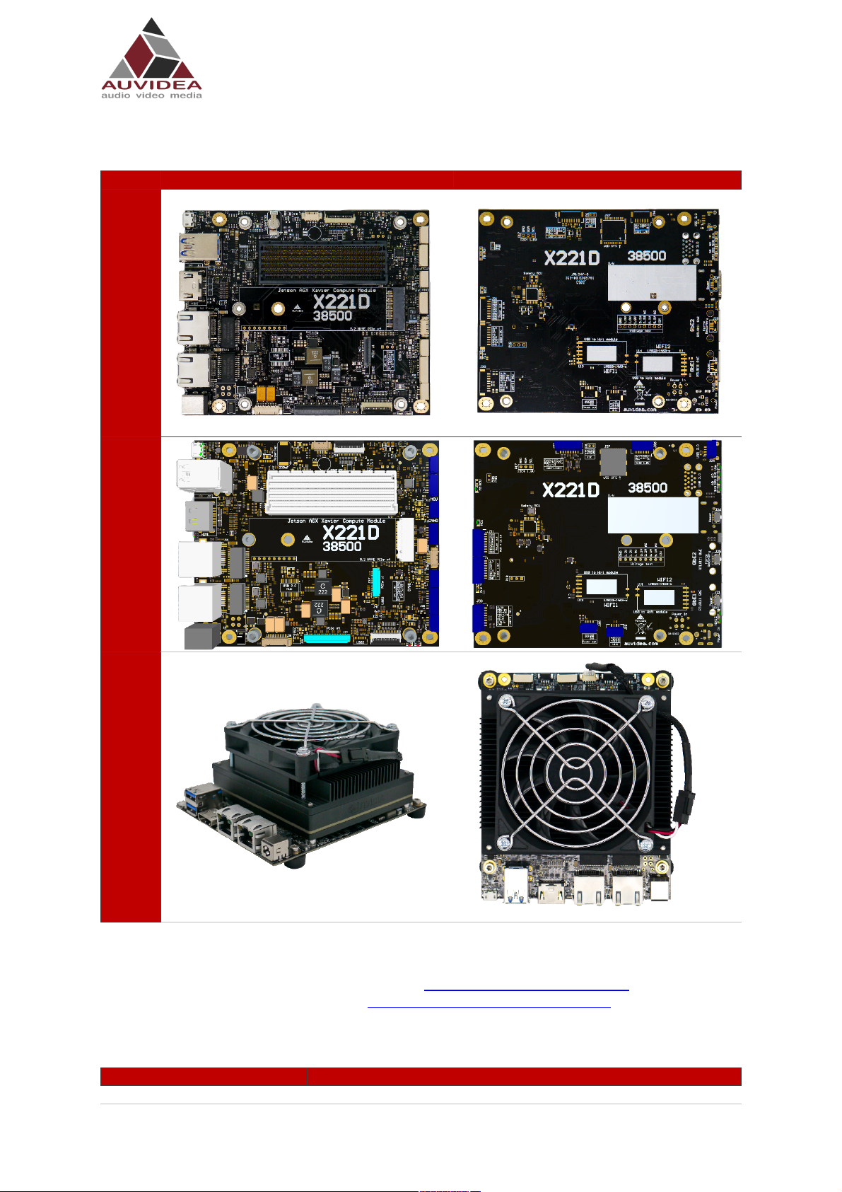
3.4 Model pictures ............................................................................................................................................. 8
3.5 Power consumption and efficiency .............................................................................................................. 8
SECTION 4 Features ...................................................................................................... 11
4.1 Crypto authentication chip ........................................................................................................................ 11
4.2 Fan connection ........................................................................................................................................... 11
4.3 Manufacturing options .............................................................................................................................. 12
SECTION 5 Pinout description top side ......................................................................... 13
5.1 J1 – Power jack ........................................................................................................................................... 13
5.2 J2 – Power port .......................................................................................................................................... 13
5.3 J3 – USB3 .................................................................................................................................................... 13
5.4 J4 – Ethernet .............................................................................................................................................. 13
5.5 J5 – CAM_LED ............................................................................................................................................. 13
5.6 J6 – CAN1 ................................................................................................................................................... 14
5.7 J7 – I2C ....................................................................................................................................................... 14
5.8 J8 – FAN ...................................................................................................................................................... 14
5.9 J10 – Debug port ........................................................................................................................................ 14
5.10 J11 – HDMI ................................................................................................................................................. 15
5.11 J12 – CAN0 ................................................................................................................................................. 15
5.12 J14 – MCU .................................................................................................................................................. 15
5.13 J15 – 2x USB 3.1 ......................................................................................................................................... 16
5.14 J17 – MICRO USB ........................................................................................................................................ 16
5.15 J19 – CSI-2 .................................................................................................................................................. 16
5.16 J20 – PCIe x4 ............................................................................................................................................... 17
5.17 J22 – ETHERNET ......................................................................................................................................... 18
5.18 J24 – CSI-1 .................................................................................................................................................. 18
5.19 J28 – SPI ..................................................................................................................................................... 19
5.20 J33 – I2C ..................................................................................................................................................... 20
5.21 J37 – PCIe x1 ............................................................................................................................................... 20
5.22 J38 – VCC_SRC ............................................................................................................................................ 21
5.23 J39 – USB2 .................................................................................................................................................. 21
5.24 J41 – USB2 .................................................................................................................................................. 21
5.1 RGB LED ...................................................................................................................................................... 21
SECTION 6 Pinout description bottom side ................................................................... 22
6.1 J18 – WiFi ................................................................................................................................................... 22

X221D & X221D-AI TECHNICAL REFERENCE MANUAL
VERSION: 1.0
Page 3 of 39
Jan.2023
6.2 J21 – Power button .................................................................................................................................... 22
6.3 J23 – I2S3 ................................................................................................................................................... 22
6.4 J25 – Force recovery button ....................................................................................................................... 22
6.5 J26 – Reset button ..................................................................................................................................... 22
6.6 J27 – MicroSD UFS ...................................................................................................................................... 22
6.7 J29 – USB 2.0 .............................................................................................................................................. 22
6.8 J30 – UART5 + MCU .................................................................................................................................... 22
6.9 J31 – Power out .......................................................................................................................................... 23
6.10 J32 – UART1/I2C3 ....................................................................................................................................... 23
6.11 J35 – Power out .......................................................................................................................................... 23
6.12 J36 – I2S2 ................................................................................................................................................... 24
6.13 U13 – LM823-1463 bay .............................................................................................................................. 24
6.14 U14 – LM823-1463 bay .............................................................................................................................. 24
6.15 P6 – Jumper ................................................................................................................................................ 24
6.16 P17 – I2C4 .................................................................................................................................................. 24
6.17 P18 – Alternativ power button and monitoring pin ................................................................................... 24
SECTION 7 Frequently Asked Questions ....................................................................... 25
SECTION 8 Disclaimer ................................................................................................... 26
SECTION 9 Copyright notice ......................................................................................... 27
SECTION 10 Appendix A [CSI-Cameras] ........................................................................... 28
10.1 Camera connection example ..................................................................................................................... 28
10.2 Test CSI-Camera functionality .................................................................................................................... 29
SECTION 11 Appendix B [GPIO] ...................................................................................... 30
11.1 GPIO control ............................................................................................................................................... 30
SECTION 12 Appendix C [I2C] ......................................................................................... 32
12.1 I2C device bus ............................................................................................................................................ 32
12.2 I2C usage of devices and registers ............................................................................................................. 32
SECTION 13 Appendix D [SSD-Boot] ............................................................................... 34
SECTION 14 Appendix E [Wi-Fi] ...................................................................................... 35
14.1 Options from AUVIDEA .............................................................................................................................. 35
14.2 Options from other sources ....................................................................................................................... 37
14.3 DIY integration ........................................................................................................................................... 37
14.4 Test Wi-Fi module connection ................................................................................................................... 39

X221D & X221D-AI TECHNICAL REFERENCE MANUAL
VERSION: 1.0
Page 4 of 39
Jan.2023
SECTION 1 Document revisions and changes
Document
version
Changes
0.1
Initial document, internal verification process
0.3
Reduced board variety, fixed appendix B,
0.4
Added AI Version and bottom pinout description and information about swapped
labels for J5 and J28

X221D & X221D-AI TECHNICAL REFERENCE MANUAL
VERSION: 1.0
Page 5 of 39
Jan.2023
SECTION 2 Product revisions and changes
Product
version
Changes
38500

X221D & X221D-AI TECHNICAL REFERENCE MANUAL
VERSION: 1.0
Page 6 of 39
Jan.2023
SECTION 3 Overview
3.1 Introduction
The X221D is intended to be a great development platform with
These systems let you dive into AI with ease. They allow you to explore AI applications like people
detection, face masking and more. The full suite of NVIDIA SDKs may be installed. At your choice
these systems may be equipped with the entire family of NVIDIA compute modules with the AGX
Xavier form factor.
The X221D features an industrial strength design and is commercially deployable in any volume.
3.2 Carrier board features
X221D only components on top side
X221D-AI (All In) top and bottom parts
Description
X221D
X221D-AI
Operating Voltage
12V
12V
Jetson power modes
30W + MAXN
30W + MAXN
Supported modules
AGX-Xavier, AGX-Xavier-Industrial
Supported module configurations
Configuration 2
Configuration 2
Super Cap UPS
(optional)
(optional)
RTC super cap
200mF
200mF
Rechargeable lithium cell (MS621FE)
(optional)
(optional)
Power out (12V, 5A)
yes
Yes (J31)
Power/Reset/Force-Recovery Buttons
-
yes
Revers voltage protection
yes
yes
Overvoltage protection
yes
yes
HDMI out
1x
1x
USB 2.0
1x microUSB
1xquad USB2.0 hub:
(1: J3, 2: J41, 3: U14(LM823), 4:
U13(LM823) or J39)
1x microUSB
USB 3.0
2xUSB-A(J15)
+1xFPC(J3)
2xUSB-A(J15)
+1xFPC(J3)
Safety MCU (for JAXi)
-
yes
Basic MCU
yes
-
GbE (RJ45)
2x RTL8111 (PCIe to Gbe)
WIFI
-
- (2x optional LM823-1463)
MicroSD/UFS card slot
-
1x (only SD-Card mode, no UFS)
CAN (RX/TX only)
1x
1x
CAN
1x
1x
UART5
-
1x (J30)
I2S2
-
1x
I2S3
-
1x
I2C
2x
2x
I2C4
-
1x
PCIe x4/I2C combo
1x
1x
PCIe x1
1x
1x
CSI
2x
2x
Auto flashing
yes
yes
Debug port
yes (J10)
yes (J10)

X221D & X221D-AI TECHNICAL REFERENCE MANUAL
VERSION: 1.0
Page 7 of 39
Jan.2023
3.3 Technical specification
Description
Note
HDMI
2.0, 4k60p
USB 3.1
10Gb/s
Physical size
125mm x 104.6mm
3D STP model available
Mounting holes
For 4x M3
Temperature range
-25°C to +70°C
Cold temperature monitoring
with MCU optional
Humidity
Noncondensing humidity
Longevity
Very good
No temperature sensitive
electrolytic capacitors
Fan connector (5V, PWM)
1x
1x
RGB LED (GPIO controlled)
yes
yes
Crypto authentication chip
- (planned for rev. 3)

X221D & X221D-AI TECHNICAL REFERENCE MANUAL
VERSION: 1.0
Page 8 of 39
Jan.2023
3.4 Model pictures
The heatsink is designed for the AGX Xavier & AGX Xavier Industrial & AGX Orin. It is designed to mount a
standard 80x80mm fan. A production version is available. The Heatsink is not included with the base board.
Sets may be available.
Pleas see our Heatsink and Fan solution on our website: https://auvidea.eu/product/70861/
Or our Product Brief for the Heatsink and Fan: https://auvidea.eu/download/D70861.pdf
3.5 Power consumption and efficiency
Description
X221D & X221D-AI
Carrier board logic
1-2W
Top side
Bottom side
X221D
X221D-
AI
X221D
with
module
and
cooler

X221D & X221D-AI TECHNICAL REFERENCE MANUAL
VERSION: 1.0
Page 9 of 39
Jan.2023
1.8/3.3/5V power converter
efficiency
>90%
Power in converter efficiency
-
3.6 Carrier board comparison
Auvidea provides a variety of compatible boards for the AGX Xavier an AGX Orin. The following table
tries to help you find the best fitting carrier board for your needs. For more in depth information
about each board pleas see the respective manual.
Description
AGX Xavier compatible
AGX Orin compatible
The
X221
X230
The D-series (developer series) offers
X221D
X230D
This carrier board is similar to the X230D series
adding a PCIex8 connector
X231
The following table shows the features and differences in more detail.
AGX Xavier
AGX Xavier
AGX Orin
AGX Orin
Compatible board
X220
X221D
X230D
X230
Recommended
configuration
conifg 2
conifg 2
conifg 2
conifg 2
UPHY_RX0/TX0
PCIe x1
PCIe x1 FPC
GbE 2
UPHY_RX1/TX1
USB 3 (ext.
optional)
USB 3 FPC 12p
USB 3 Type A
USB 3 Type A
UPHY_RX20/TX20
USB 3 Type A
USB 3 Type A
UPHY_RX21/TX21
GbE 1
GbE 1
UPHY_RX22/TX22
GbE 2
M.2 NVME (C4), RP
UPHY_RX23/TX23
UPHY_RX10/TX10
UFS
UFS
UPHY_RX11/TX11
USB 3 Type A
USB 3 Type A
UPHY_RX11/TX11
M.2 NVME
M.2 NVME
M.2 NVME
PCIe x8 (C5), RP/EP
UPHY_RX13/TX13
UPHY_RX14/TX14
UPHY_RX15/TX15
UPHY_RX16/TX16
UPHY_RX17/TX17
UPHY_RX18/TX18
UPHY_RX19/TX19
UPHY_RX2/TX2
PCIe x4 on
extension
connector (for
38451 add-on)
PCIe x4 FPC (J20)
PCIe x4 FPC (J20)
PCIe x8 (C7), RP/EP
UPHY_RX3/TX3
UPHY_RX4/TX4
UPHY_RX5/TX5
UPHY_RX6/TX6
USB 3 Type A
USB 3 Type A
UPHY_RX7/TX7
GbE 1
GbE 1
UPHY_RX8/TX8
GbE 2
GbE 2
UPHY_RX9/TX9
HDMI_DP2
HDMI
HDMI
HDMI
HDMI

X221D & X221D-AI TECHNICAL REFERENCE MANUAL
VERSION: 1.0
Page 10 of 39
Jan.2023
CSI-0 & CSI-1
CSI-AB
CSI-AB
CSI-AB
CSI-AB
CSI-6 & CSI-7
CSI-CD
CSI-CD
CSI-CD
CSI-CD
supported by X221
when usinga AGX
Orin module
supported by X221
when usinga AGX
Orin module

X221D & X221D-AI TECHNICAL REFERENCE MANUAL
VERSION: 1.0
Page 11 of 39
Jan.2023
SECTION 4 Features
4.1 Crypto authentication chip
Pin
Description
Model
ATSHA204A-SSHDA-T
Datasheet
https://ww1.microchip.com/downloads/en/DeviceDoc/ATSHA204A-Data-
Sheet-40002025A.pdf
The crypto chip can be used for authentication, software licensing and copy protection.
The crypto authentication chip is currently not supported. Support is planned for revision 3 of this
product.
4.2 Fan connection
4.2.1 Fan + Adapter specification
4.2.2 Set Fan speed
Set FAN speed to lowest value. Some FANs don't stop when speed is 0.
echo 0 > /sys/devices/pwm-fan/target_pwm
Set FAN speed to highest value possible
echo 255 > /sys/devices/pwm-fan/target_pwm
4.2.3 Read Fan speed
command to read FAN tachometer. Value displays in rounds per minute.
(Depending on the FAN this value may need to be scaled/converted)
Image
Note
X221D +
Fan
On the left you see a standard
80x80x15mm fan connected with the
adapter cable to the J8 Fan connector.
Adapter
cable
On the left you see a drawing of the
adapter Kable and the pin description.

X221D & X221D-AI TECHNICAL REFERENCE MANUAL
VERSION: 1.0
Page 12 of 39
Jan.2023
cat /sys/devices/generic_pwm_tachometer/hwmon/hwmon1/rpm
4.3 Manufacturing options
4.3.1 Enclosure
Auvidea can provide custom enclosures for its carrier boards. These enclosures provide a passively
cooled solution. This solution is designed for the AGX models. With a max power draw of 35W
(normal mode) the enclosure temperature reaches 55C° while in 24°C room temperature which is a
safe temperature for Human contact.
The MaxN mode (up to 90W) is not recommended as the enclosure temperature increases above
acceptable levels for direct human contact.
It is also possible to apply your branding on the front and back Plate of the Enclosure. Auvidea has
inhouse capabilities of laser and milling engraving.
4.3.2 Branding and QR codes
Besides the branding options for the enclosure, it is also possible to customize the label field on the
carrier board.
Auvidea uses the label field to engrave a small QR code and serial number to track production
processes.
It is possible to add your custom engravings like logos, text or QR codes to this field.
A laser engraver is used.
4.3.3 Custom configurations
The standard carrier board configuration is designed to suit most use cases.
Please see the Pinout description for customization examples like voltage configurations (3.3V or
1.8V).
We take pride in tailoring our products to your special need and are capable to adjust it in small
production series. Please contact Auvidea with your special requests to work out a solution.
Image
Note
In the left image the label field is
highlighted.

X221D & X221D-AI TECHNICAL REFERENCE MANUAL
VERSION: 1.0
Page 13 of 39
Jan.2023
SECTION 5 Pinout description top side
5.1 J1 – Power jack
Barrel plug.
12V Input, please use a high quality power supply for stable operation.
5.2 J2 – Power port
Molex MicroFit 3.0 (alternative power input)
5.3 J3 – USB3
Pin
Description
Socket pin
Note
1
VUSB3-3
??
3.3V (how to control power supply?)
2
VUSB3-3
??
3.3V
3
USB2_D_N
A11
4
USB2_D_P
A10
5
GPIO22
F54
6
GND
7
UPHY_RX1_N
C22
8
UPHY_RX1_P
C23
9
GND
10
UPHY_TX1_N
G22
11
UPHY_TX1_P
G23
12
GND
5.4 J4 – Ethernet
RJ45
Standard pinout.
5.5 J5 – CAM_LED
Pin
Description
Socket pin
Note
1
VCC_SRC
Max 1A
2
VDD_5V
Max 1A
3
GPIO35_PWM3
L50
Low side switch to GND, can be controlled with
GPIO35_PWM3 or CAM1-MCLK (1.8-5V) or CAM2-MCLK (1.8-
5V) (please see schematic image), Max 3.7A
4
GND
Please note that on REV 2 and below the J5 and J28 label printed on the pcb is swapped, this mistake
is fixed in newer revisions.
Q13 (pin 3) is not over current protected (Max 3.7A).
Set GPIO35_PWM3 too low to activate Q13 (pin3).
As you can see you can control the J5 pin 3 with three options.
The CAM1 and CAM2 control are intended to be set by your camera device

X221D & X221D-AI TECHNICAL REFERENCE MANUAL
VERSION: 1.0
Page 14 of 39
Jan.2023
5.6 J6 – CAN1
JST-GH 1.25mm
Pin
Description
Socket pin
Note
1
NC
Not powered
2
CAN1_TX
H61
2.5V center voltage, with CAN transceiver
3
CAN1_RX
B61
2.5V center voltage, with CAN transceiver
4
GND
CAN1 is RX/TX only and is not outputting power
5.7 J7 – I2C
PicoBlade 1.25mm
Pin
Description
Socket pin
Note
1
3.3V
2
SCL
J61
3.3V, open drain
3
SDA
K61
3.3V, open drain
4
GND
5.8 J8 – FAN
PicoBlade 1.25mm
Pin
Description
Socket pin
Note
1
GND
2
12V
1A
3
TACH
E54
1.8V input 100K pull up to 1.8V, fan speed tacho
4
PWM
K62
open drain output with 10k pullup to 12V
For the use of a 5V fan there is an option to resolder a component appropriately.
5.9 J10 – Debug port
JST-GH 1.25mm
Pin
Description
Socket pin
Note
1
3.3V
2
UART3_TX
H62
3.3V, AGX Xavier debug console transmit

X221D & X221D-AI TECHNICAL REFERENCE MANUAL
VERSION: 1.0
Page 15 of 39
Jan.2023
3
UART3_RX
K60
3.3V, AGX Xavier debug console receive
4
GPIO13_OUT
G7
3.3V, G7 (AGX Xavier ball), output from Jetson
5
GPIO4_IN
B59
3.3V, B59 (AGX Xavier ball), input to Jetson
6
GND
5.10 J11 – HDMI
Standard pinout, connected to DP-2
5.11 J12 – CAN0
JST-GH 1.25mm
Pin
Description
Socket pin
Note
1
5V
C61
max 500mA (with current limiting switch), can be controlled with
CAN0_STBY (GPIO09), socket pin C61 with low = on, high = off, pin
is also reverse power protected
2
CAN0_H
F58
2.5V center voltage, with CAN transceiver
3
CAN0_L
D59
2.5V center voltage, with CAN transceiver
4
GND
You can set a solder ball to enable 120Ohm Termination resistor as shown in the picture below.
5.12 J14 – MCU
JST-GH 1.25mm
Pin
Description
Socket pin
Note
1
3.3V
2
MCU_TX
3.3V, MCU console debug port, transmit, 115200 baud, 8N1
3
MCU_RX
3.3V, MCU console debug port, receive, 115200 baud, 8N1
4
SWCLK
ST-Link programming interface of MCU
5
SWDIO
ST-Link programming interface of MCU
6
GND
With the AI model of the X221 you have access to the safety MCU features. Please contact Auvidea
for more information.
The basic MCU of the non AI models only handle power up functionality.

X221D & X221D-AI TECHNICAL REFERENCE MANUAL
VERSION: 1.0
Page 16 of 39
Jan.2023
5.13 J15 – 2x USB 3.1
Nexus-3815RFY
Pin
Description
Socket pin
Note
1
Vin
1A, 5V
2
USB3_D_N
G10
3
USB3_D_P
G11
4
GND
5
UPHY_RX11_N
D13
6
UPHY_RX11_P
D12
7
GND
8
UPHY_TX11_N
H13
9
UPHY_TX11_P
H12
10
Vin
1A, 5V
11
USB1_D_N
C10
12
USB1_D_P
C11
13
GND
14
UPHY_RX6_N
B17
15
UPHY_RX6_P
B16
16
GND
17
UPHY_TX6_N
K16
18
UPHY_TX6_P
K17
19
GND
20
GND
21
GND
22
GND
Standard pinout (type A).
10Gb/s.
Power can be Enabled/Disabled with GPIO22
5.14 J17 – MICRO USB
Standard pinout.
Host and device mode supported.
Powered by power limiting switch with 500mA.
Alternatively, you can use the J29 connector, using the same pins.
5.15 J19 – CSI-2
Pin
Description
Socket pin
Note
1
VDD_3V3
3.3V
2
SDA-1
Connected to I2C_GP2_Dat_LVS or I2C_GP2_DAT depending
on config. I2C bus number 1.
3
SCL-1
Connected to I2C_GP2_CLK_LVS or I2C_GP2_CLK depending
on config. I2C bus number 1.
4
GND
5
CAM1_MCLK
J28
Connected to J28 CAM LED pin 3

X221D & X221D-AI TECHNICAL REFERENCE MANUAL
VERSION: 1.0
Page 17 of 39
Jan.2023
6
CAM1_PWDN
K57
Can be controlled with PWM01_40Pin (GPIO_07), default
configuration is high, open drain output with pullup 2.2k to
3.3V, this also connects to CAM2_PWDN.
7
GND
8
CSI_7_D1_P
C47
9
CSI_7_D1_N
C48
10
GND
11
CSI_7_D0_P
A44
12
CSI_7_D0_N
A45
13
GND
14
CSI_6_CLK_P
J44
15
CSI_6_CLK_N
J45
16
GND
17
CSI_6_D1_P
H46
18
CSI_6_D1_N
H45
19
GND
20
CSI_6_D0_P
K44
21
CSI_6_D0_N
K43
22
GND
Per special request Auvidea can manufacture the board with CAM1_PWDN and CAM2_PWDN with
pullup to 1.8V.
5.16 J20 – PCIe x4
Pin
Description
Socket pin
Note
1
VDD_3V3
3.3V
2
VDD_3V3
3.3V
3
VDD_3V3
3.3V
4
GND
5
PEX_CLK0_P
E15
6
PEX_CLK0_N
E14
7
GND
8
UPHY_TX2_P
K21
9
UPHY_TX2_N
K20
10
GND
11
UPHY_RX2_P
B21
12
UPHY_RX2_N
B20
13
GND
14
UPHY_TX3_P
H20
15
UPHY_TX3_N
H21
16
GND
17
UPHY_RX3_P
D20
18
UPHY_RX3_N
D21
19
GND
20
UPHY_TX4_P
J18
21
UPHY_TX4_N
J19
22
GND
23
UPHY_RX4_P
A18
24
UPHY_RX4_N
A19

X221D & X221D-AI TECHNICAL REFERENCE MANUAL
VERSION: 1.0
Page 18 of 39
Jan.2023
25
GND
26
UPHY_TX5_P
G19
27
UPHY_TX5_N
G18
28
GND
29
UPHY_RX5_P
C19
30
UPHY_RX5_N
C18
31
GND
32
PEX_WAKE_N
A8
33
PEX_L0_RST_N
D10
34
GND
35
I2C_GP2_DAT_LVS
???
36
I2C_GP2_CLK_LVS
???
37
PEX_L0_CRQ_N
E11
38
VDD_3V3
3.3V
39
VDD_3V3
3.3V
40
VDD_3V3
3.3V
5.17 J22 – ETHERNET
Standard pinout.
5.18 J24 – CSI-1
Pin
Description
Socket pin
Note
1
VDD
3.3V (5V see instructions)
2
FT-SDA
Connected to FT_SDA or I2C_GP5_DAT depending on
configuration (what is standard?)
3
FT-SCL
Connected to FT_SCL or I2C_GP5_CLK (gibt kein
GP5!!!)depending on configuration
4
GND
5
CAM2_PWDN
F57
Can be controlled with PWM01_40Pin (GPIO_07, socket pin
F57), default configuration is high, open drain output with
pullup 2.2k to 3.3V, this also connects to CAM1_PWDN
6
CAM2—MCLK
Connected to J28 CAM LED pin 3
7
GND
8
CSI_1_D1_P
J41
9
CSI_1_D1_N
J42
10
GND
11
CSI_1_D0_P
G41
12
CSI_1_D0_N
G42
13
GND
14
CSI_0_CLK_P
F43
15
CSI_0_CLK_N
F42
16
GND
17
CSI_1_D1_P
E39
18
CSI_1_D1_N
E38
19
GND
20
CSI_0_D0_P
E42

X221D & X221D-AI TECHNICAL REFERENCE MANUAL
VERSION: 1.0
Page 19 of 39
Jan.2023
21
CSI_0_D0_N
E41
22
GND
Per special request Auvidea can manufacture the board with CAM1_PWDN and CAM2_PWDN with
pullup to 1.8V.
CSI default voltage is 3.3V but it can be changed to 5V. To perform this modification, you need to
move the bead from the 3.3V location (marked with the number 3 as shown in the picture) to the 5V
location (marked with the number 5 as shown in the picture).
The same process applies to I2C where you must move two beads to the desired location of 1.8
(1.8V) or 3.3 (3.3V).
This modification should be performed with care and some good soldering skills.
Auvidea does not cover damages inflicted by poorly performed modifications.
Please contact Auvidea for custom configurations.
5.19 J28 – SPI
SM08B-GHS-TB
Pin
Description
Socket pin
Note
1
VDD_5V
5V
2
VDD_3V3
3.3V
3
VDD_1V8
1.8V
4
SPI1_CS0
E55
5
SPI1_SCK
J57
6
SPI1_MOSI
D55
7
SPI1_MISO
A56
8
GND
Please note that on REV 2 and below the J5 and J8 label printed on the pcb is swapped, this mistake
is fixed in newer revisions.

X221D & X221D-AI TECHNICAL REFERENCE MANUAL
VERSION: 1.0
Page 20 of 39
Jan.2023
5.20 J33 – I2C
Pin
Description
Socket pin
Note
1
VDD_5V
5V, overvoltage protected
2
FT_SCL
???
overvoltage protected
3
FT_SDA
???
overvoltage protected
4
GND
5.21 J37 – PCIe x1
Pin
Description
Socket pin
Note
1
GND
2
GPIO17_40HEADER
A54
3
PEX_WAKE_N
A8
4
GND
5
PEX_L1_CRQ_N
D9
6
PEX_L1_RST_N
B9
7
GND
8
UPHY_RX0_N
A23
9
UPHY_RX0_P
A22
10
GND
11
UPHY_TX0_N
J23
12
UPHY_TX0_P
J22
13
GND
14
PEX_CLK1_N
F17
15
PEX_CLK1_P
F16
16
GND
17
VDD_3V3
3.3V
18
VDD_3V3
3.3V
19
GND
20
VDD_5V
5V
21
VDD_5V
5V
22
GND
Other manuals for X221D
1
This manual suits for next models
1
Table of contents
Other Auvidea Computer Hardware manuals
Popular Computer Hardware manuals by other brands

Brook
Brook P5 Plus FIGHTIG BOARD user guide

VIA Technologies
VIA Technologies SOM-6X80 user manual

Nuvoton
Nuvoton NuSpeech Series Technical reference manual

Cisco
Cisco SCE8000 GBE Removal and replacement procedures

Gigabyte
Gigabyte GC-WIFI7 installation guide

Crown
Crown PIP-BEQ Quick reference & setup guide

National Instruments
National Instruments NI 6711 user manual

Supermicro
Supermicro AOC-IBH-X6HS user guide

QSC
QSC USL JSD-60 user manual

General Standards Corporation
General Standards Corporation PCI-DIO24PMC-DIO24PCI-DIO24-GD1 user manual

SIIG
SIIG JJ-EC2011-S1 Quick installation guide

Matrox
Matrox Extio Series user guide