Auvidea JNX30-LC Product manual

AUVIDEA
JNX30-LC
TECHNICAL
REFERENCE
MANUAL
SCOPE OF WORK
Providing technical information and documentation to the product line JNX30-LC for NVIDIA
Jetson Nano, TX2 NX & Xavier NX
PCB NUMBER
38401
ISSUE DATE [REVISED DATE]
DEC.2021 [DEC.2021]
Version
1.2
PAGES
28

JNX30-LC TECHNICAL REFERENCE MANUAL
VERSION: 1.2 Page 2 of 28 DEC 2021
CONTENTS
SECTION 1 Document revisions and changes ................................................................ 4
SECTION 2 Product revisions and changes .................................................................... 5
2.1 Product versions .......................................................................................................................................... 5
2.2 Design and manufacturing........................................................................................................................... 5
SECTION 3 Overview .................................................................................................... 6
3.1 Jetson compute module .............................................................................................................................. 6
3.2 JNX30-LC ...................................................................................................................................................... 6
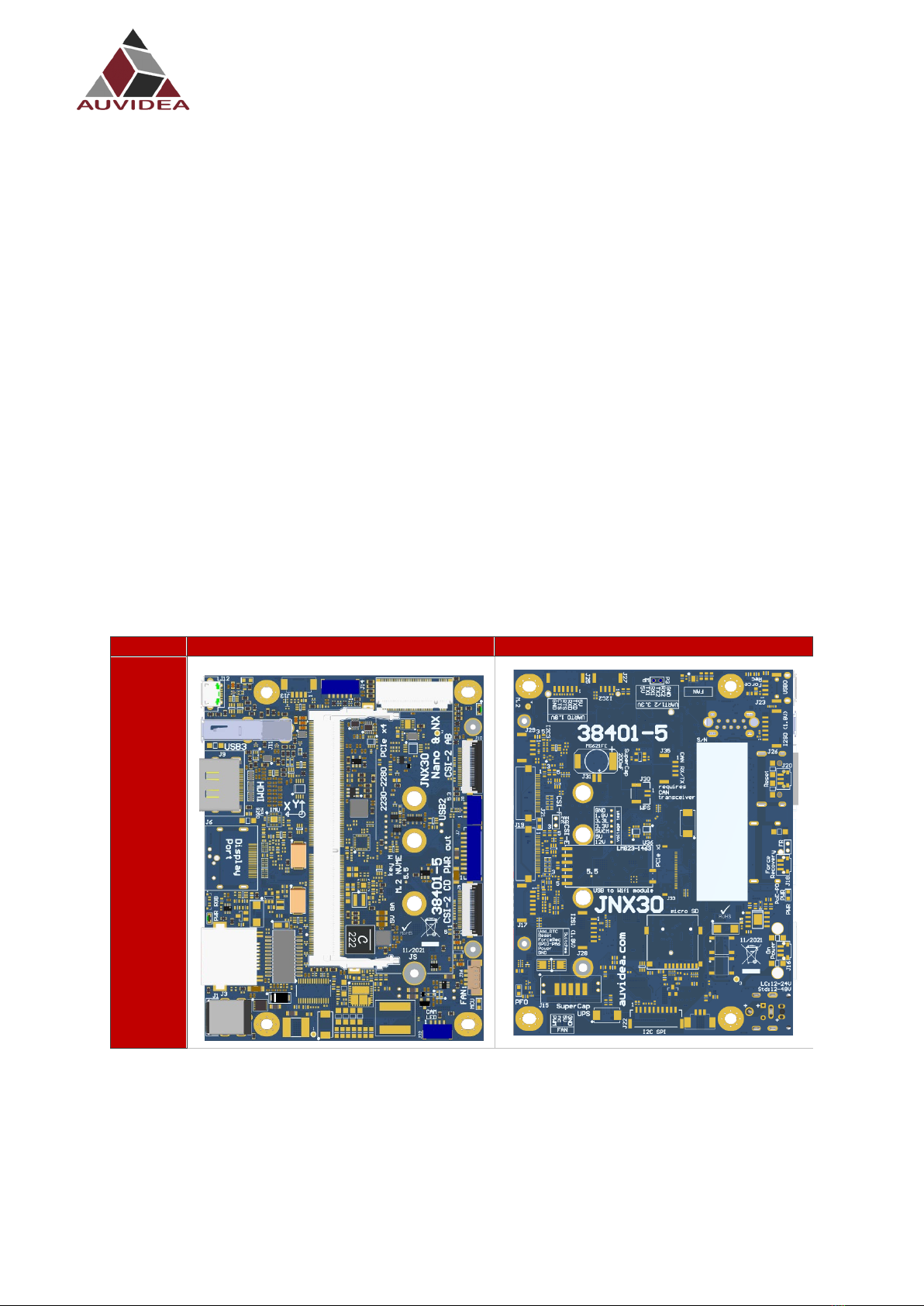
3.3 Model pictures............................................................................................................................................. 6
3.4 JNX30-LC features and comparison ............................................................................................................. 7
3.5 Technical specifications ............................................................................................................................... 8
3.6 Power consumption..................................................................................................................................... 8
SECTION 4 Features...................................................................................................... 9
4.1 Booting via SSD ............................................................................................................................................ 9
4.2 Crypto chip................................................................................................................................................... 9
4.3 MCU ............................................................................................................................................................. 9
SECTION 5 Pinout description......................................................................................10
5.1 J1 - Power input jack.................................................................................................................................. 10
5.2 J3 - Ethernet (GbE) ..................................................................................................................................... 10
5.3 J4 - M.2 PCIEx4 NVME SSDs ....................................................................................................................... 10
5.4 J5 - CSI-2 CD ............................................................................................................................................... 11
5.5 J7 – Power out ........................................................................................................................................... 12
5.6 J8 - USB 2.0 ................................................................................................................................................ 12
5.7 J9 - HDMI.................................................................................................................................................... 12
5.8 J10 - CSI-2 AB ............................................................................................................................................. 13
5.9 J11 - USB 3.0 – 3.1...................................................................................................................................... 13
5.10 J12 - Micro USB .......................................................................................................................................... 13
5.11 J14 - UART connector................................................................................................................................. 14
5.12 J32 – CAM LED ........................................................................................................................................... 14
5.13 J36 - Fan connector.................................................................................................................................... 14
5.14 U1 - Crypto chip ......................................................................................................................................... 15
5.15 LED - PWR .................................................................................................................................................. 15
SECTION 6 FAQ ...........................................................................................................16
SECTION 7 Disclaimer..................................................................................................17
SECTION 8 Copyright notice.........................................................................................18
SECTION 9 Appendix A [CSI-Cameras]..........................................................................19
9.1 Connection examples................................................................................................................................. 19

JNX30-LC TECHNICAL REFERENCE MANUAL
VERSION: 1.2 Page 3 of 28 DEC 2021
SECTION 10 Appendix B [GPIO] .....................................................................................21
10.1 Calculate GPIO pins.................................................................................................................................... 21
10.2 GPIO control .............................................................................................................................................. 21
SECTION 11 Appendix C [I2C] ........................................................................................23
11.1 I2C Examples of configurations and how to use........................................................................................ 23
SECTION 12 Appendix D [Install Jetpack] .......................................................................24
12.1 Installed Packages...................................................................................................................................... 24
SECTION 13 End of document........................................................................................28

JNX30-LC TECHNICAL REFERENCE MANUAL
VERSION: 1.2 Page 4 of 28 DEC 2021
SECTION 1 Document revisions and changes
Document
version
Changes
V1.0
initial document, internal verification process
V1.1
internal verification process
V1.2
first release version

JNX30-LC TECHNICAL REFERENCE MANUAL
VERSION: 1.2 Page 5 of 28 DEC 2021
SECTION 2 Product revisions and changes
2.1 Product versions
Product
version
Changes
38401-2
added 5V 8A power supply
added PCIe connector (rotate it compared to rev 1)
added CAN connector (requires external CAN transceiver module - 38163-3)
38401-3
changed MCU footprint from TSSOP-20 to UFQFN-28
supports STM32F042G6U6 and STM32L031G6U6 - dual rail power
added support for MCU flashing from Jetson via UART
changed R110 to 3.01k for maximum input current of 6A
changed main power supply from LT8646 to MIC28514
extended e-fuse support for TPS26630/1 type
added 2nd FAN connector
38401-4
internal release
38401-5
changed 3.3V power supply and power it by 12V
changed MCU LDO (absolute max. input voltage 26V)
added discrete components for power up (no MCU)
moved FAN connector, so that it can be directly plugged
changed over current protection from chip to fuse
2.2 Design and manufacturing
Flexible design and manufacturing
designed and manufactured in Germany
in-house fully automated production line with 3D AOI
special configuration possible with minimum purchase of 25 pcs (display port, M.2, PoE, 48V power
in, super cap option, 2 RPi camera module connectors, SPI, I2C, switches, etc.)
design services: you architect your custom carrier board and Auvidea designs and produces it - please
ask for a quote.

JNX30-LC TECHNICAL REFERENCE MANUAL
VERSION: 1.2 Page 6 of 28 DEC 2021
SECTION 3 Overview
3.1 Jetson compute module
This new JNX30-LC carrier board has been designed for the Jetson Xavier NX primarily, but it also
supports the TX2 NX and Nano compute modules. A 5V 8A on-board power converter supports the
high-power modes of the NX.
3.2 JNX30-LC
Easy integration into passively cooled systems
Easy flashing: just connect a USB OTG cable (AutoFlash)
High performance storage: M.2 NVME PCIe x4
Applications
Industrial AI computers
Digital signage systems
3.3 Model pictures
Top side
Bottom side
JNX30-LC

JNX30-LC TECHNICAL REFERENCE MANUAL
VERSION: 1.2 Page 7 of 28 DEC 2021
3.4 JNX30-LC features and comparison
Description
JNX30-LC
NVIDIA Devkit
Power
6V - 19V (barrel connector)
5V – 19V
NX powering
5V 8A power supply
?
DP
no (optional with some JNX30-LC versions)
yes
HDMI
yes
yes
Fan connector
yes
yes
M.2 NVME Key M
yes
yes
Micro SD card
no (optional with other models)
no
M.2 Key E
only with external module
(using internal USB - J8)
yes
CAN RX / TX
no (optional with other models)
yes
USB 3
1x USB 3.1
(native - full performance)
4x USB 3.1
(via USB hub - shared)
Micro USB
1x Micro USB
(device mode only)
1x Micro USB
(device mode only)
Auto Flashing
yes
(plug in host cable and flash)
no
USB 2.0
1x USB 2.0 (JST-GH, J8)
no
Ethernet
Gigabit RJ45 (2 LEDs)
PoE option
no
yes - J19
CSI
2x CSI-2 (4 lanes) plus camera LED
(hardware sync available)
2x CSI-2
UART
2x (J14)
2x (40 pin header, P12)
I2C
no (2x optional with some JNX versions)
2x (40 pin header, P12)
I2S
no (2x optional with some JNX versions)
1x (40 pin header, P12)
SPI
no (optional with some JNX30 versions)
2x (40 pin header)
Additional features
Protection
overvoltage protection (TVS diode)
?
Level shifters unidirectional level shifters (work better)
bi-directional (sometimes
cause problems)
Buttons
no
12 pin header
Expandability
1. Fully populated variants available
no
2. Add-on boards for more USB and
Ethernet
3. IMU
4. board EEPROM and crypto chip (for SW
copy protection)
5. PCIe x1 connector
6. LM823 WIFI module
7. 2 more CSI-2 interfaces (2 lanes each)
8. Micro SD card
9. RTC battery (rechargeable)
10. Over current fuse (product safety)
11. UPS option for graceful power down
12. On board MCU for watchdog and
remote power cycle (LTE)

JNX30-LC TECHNICAL REFERENCE MANUAL
VERSION: 1.2 Page 8 of 28 DEC 2021
3.5 Technical specifications
Description
Note
HDMI
standard HDMI connector (2.0)
USB 3.0/3.1
5Gb/s (dependent on compute module)
Physical size
80 x 104.6mm
Mounting holes
4x M3
Temperature range
0 to 70°C (extended temperature range optional)
Humidity
noncondensing
Longevity
Very long as no temperature sensitive components
are used (like electrolytic capacitors)
3.6 Power consumption
Description
JNX30-LC
Carrier board logic
< 1 watt
3.3/5V power converter efficiency
> 90%
Power in converter efficiency
n.a.

JNX30-LC TECHNICAL REFERENCE MANUAL
VERSION: 1.2 Page 9 of 28 DEC 2021
SECTION 4 Features
4.1 Booting via SSD
Auvidea ships some development systems with a pre-configured SSD. This contains a bootable
partition which can be larger than the storage capacity of the integrated eMMC flash memory on the
compute module. This allows the installation of all tools and supporting applications in the boot
partition:
Linux
Jetpack 4.x
A large selection of SDKs like listed in appendix D (CUDA, VisionWorks, DeepStream and
more)
3rd party applications and demo programs
Sample video files to immediately try out the AI models
The SSD typically included is a 128GB NVME SSD by Transcend (model: TS128GMTE110S). It offers
very high performance as it connects to the compute module with 4 PCIe Gen2 lanes (5 Gbit/s).
Installation:
Full length 2280 SSDs must be inserted carefully as the SO-DIMM socket of the compute module
blocks tilting. Please slide the SSD in carefully from the side and ensure, that it is seated properly
before applying power. Secure the SSD with a M3 (nylon) screw. Metal screws must be treated with
care, so that the head of the screw is small enough that it does not touch any traces or components
on the compute module
High power SSDs may require extra cooling by installing a thermal pad between the SSD and the
compute module or the carrier board.
4.2 Crypto chip
The crypto chip has been added to support software licensing and copy protection. Please check the
data sheet of the manufacturer for details.
Model: ATSHA204A-MAHCZ-T
https://ww1.microchip.com/downloads/en/DeviceDoc/ATSHA204A-Data-Sheet-40002025A.pdf
4.3 MCU
A MCU for additional power management and watchdog functions is optional. It is standard on some of the
extended versions of the JNX30. The MCU can provide features like:
Powering control (up and down) of the compute module
Brown out protection
Clean boot after short power interruptions
Watchdog support: it can connect to the debug console of the compute module
Remote power cycle via LTE (requires LTE module with UART interface – like SIMCOM
modules)

JNX30-LC TECHNICAL REFERENCE MANUAL
VERSION: 1.2 Page 10 of 28 DEC 2021
SECTION 5 Pinout description
Please note that the software GPIO number differs from the socket pin number. This software GPIO
number must be computed with a special formula and differs between the various compute
modules. Please see appendix B for details.
5.1 J1 - Power input jack
Nexus
Pin
Description
Note
1
12V
12V nominal (absolute max. 20V)
recommend power supply 12V 36W (or higher)
Reverse voltage protection
over voltage protection (SMA6J18CA) with max 20V peak
2
GND
5.2 J3 - Ethernet (GbE)
Standard RJ45 pinout with PoE capable magnetics class 3 and 4 (PD or PSE). Connected to the
Ethernet controller on the compute module. PoE-PD and PoE-PSE are supported with the
corresponding variants of the JNX30. Also, there is the new JNX30 PDiso (38481) with isolated PoE-
PD.
5.3 J4 - M.2 PCIEx4 NVME SSDs
Please note that only NVME SSDs are supported. SATA SSDs are not supported. We recommend the
128GB Transcend SSDs (TS128GMTE110S). This SSD is standard in some of the Auvidea dev kit
offerings.

JNX30-LC TECHNICAL REFERENCE MANUAL
VERSION: 1.2 Page 11 of 28 DEC 2021
5.4 J5 - CSI-2 CD
22 pin 0.5mm pitch FPC connector
Pin
Description
Socket pin
Note
1
3.3V
Power: connected with bead to 3.3V
(5V optional if bead is moved)
2
GEN1_I2C_SDA
187
3
GEN1_I2C_SCL
185
4
GND
5
CAM2-MCLK
IN: Input - connect to 1.8V or 3.3V output of the camera to
drive the CAM LED.
1: enable CAM LED
0: disable CAM LED
6
CAM2_PWDN
206
OUT: Output (open drain with 2.2k pullup to 3.3V) - connect
to power enable of camera. The control signal is connected
via level shifting inverter to pin 152 of the compute modules.
7
GND
8
CSI_D_D1_P
66
9
CSI_D_D1_N
64
10
GND
11
CSI_D_D0_P
42
12
CSI_D_D0_N
40
13
GND
14
CSI_C_CLK_P
54
15
CSI_C_CLK_N
52
16
GND
17
CSI_C_D1_P
60
18
CSI_C_D1_N
58
19
GND
20
CSI_C_D0_P
48
21
CSI_C_D0_N
46
22
GND
Please note that on the JNX30-LC each camera connector uses its own I2C bus. This setup is different
from the NVIDIA dev kit. If you like to use CSI-2 cameras, please install the Auvidea BSP (firmware).
This CSI-2 connector has the same 22 pin pinout as the 22-pin connector on the Raspberry Pi Zero
and Raspberry Pi compute module dev kit board. With adapter cable it may connect to Raspberry Pi
camera 2.1 and Vision Component camera modules. Alvium cameras require the Alvium adapter.
Pin 6: by default, the device tree puts a PWM signal on pin 206 (LCD_BL_PWM - GPIO_07). For most
cameras (like Raspberry Pi camera with iMX219 sensor) this needs to be changed to a constant low
output to send a high to the camera for power enable. This is part of the device tree changes.
Some Vision Component camera modules use this pin to synchronise multiple cameras. The pin 5s of
all CSI-2 connectors are OR ‘red together and drive the CAM LED output.

JNX30-LC TECHNICAL REFERENCE MANUAL
VERSION: 1.2 Page 12 of 28 DEC 2021
5.5 J7 – Power out
SM10B-GHS-TB
Pin
Description
Socket pin
Note
1
V_IN
2
V_IN
3
12V
4
12V
5
12V
6
12V
7
GND
8
GND
9
GND
10
GND
5.6 J8 - USB 2.0
JST-GH 1.25mm
Pin
Description
Socket pin
Note
1
5V
2
USB2_D_N
121
3
USB2_D_P
123
4
GND
Internal USB 2.0 JST-GH connector to connect to internal USB 2.0 add-on modules (like U100, U110,
U120, etc).
5.7 J9 - HDMI
Standard pinout
CEC is not supported (pin 13 of HDMI connector)
Power pin 18 is current limited by PTC fuse (5V 50mA)

JNX30-LC TECHNICAL REFERENCE MANUAL
VERSION: 1.2 Page 13 of 28 DEC 2021
5.8 J10 - CSI-2 AB
22 pin 0.5mm pitch FPC connector
Pin
Description
Socket pin
Note
1
3.3V
Power: connected with bead to 3.3V
(5V optional if bead is moved)
2
CAM-I2C_SDA
215
3
CAM-I2C_SCL
213
4
GND
5
CAM1-MCLK
IN: Input - connect to 1.8V or 3.3V output of the camera to
drive the CAM LED.
1: enable CAM LED
0: disable CAM LED
6
CAM1_PWDN
206
OUT: Output (open drain with 2.2k pullup to 3.3V) - connect
to power enable of camera. The control signal is connected
via level shifting inverter to pin 152 of the compute modules.
7
GND
8
CSI_B_D1_P
17
9
CSI_B_D1_N
15
10
GND
11
CSI_B_D0_P
5
12
CSI_B_D0_N
3
13
GND
14
CSI_A_CLK_P
12
15
CSI_A_CLK_N
10
16
GND
17
CSI_A_D1_P
18
18
CSI_A_D1_N
16
19
GND
20
CSI_A_D0_P
6
21
CSI_A_D0_N
4
22
GND
See further details in the J5 description.
5.9 J11 - USB 3.0 – 3.1
USB 3.0 Type A standard pinout
In Rev 1: power control is always on (5V 1A)
In Rev 2 and up: Controllable with GPIO_03 (socket pin 126) power on[0]/off[1], default on[0], 5V 1A
See Appendix B for documentation on how to configure and use GPIOs.
5.10 J12 - Micro USB
Standard pinout
OTG support (to flash the compute module)
See Appendix B for documentation on how to configure and use GPIOs.

JNX30-LC TECHNICAL REFERENCE MANUAL
VERSION: 1.2 Page 14 of 28 DEC 2021
5.11 J14 - UART connector
JST-GH 1.25mm
Pin
Description
Socket pin
Note
1
5V
2
UART0_TXD
99
OUT (3.3V)
3
UART0_RXD
101
IN (3.3V)
4
UART2_TXD
236
OUT, Debug port (3.3V)
5
UART2_RXD
238
IN, Debug port (3.3V)
6
GND
Unidirectional directional 1.8V to 3.3V level shifters and 10 Ohm series resistance (plus ESD
protection).
5.12 J32 – CAM LED
Pin
Description
Socket pin
Note
1
12V
2
12V
3
CAM_LED
OUT: open drain (3.3V to 12V)
4
CAM_LED
OUT: open drain (3.3V to 12V)
CAM_LED: open drain output to drive cathode of camera LED.
Controlled by 3 signals which are OR ‘red together:
J5 pin 5 (CSI CD camera)
J10 pin 5 (CSI AB camera)
Compute module GPIO_12: (socket pin 218) 0: LED off, 1: LED on, float: LED on
CAM_LED flash signal can be used to control external camera LED. When using external LED please
limit current with external resistor. Connect cathode to CAM_LED pin and anode to 3.3V to 12V
power. Maximum current: 2A.
5.13 J36 - Fan connector
Pico blade 1.5mm
Pin
Description
Socket pin
Note
1
GND
2
5V
Max. 1A
3
TACH
-
Not connected
4
PWM
230
Open drain output with 10k pullup to 5V

JNX30-LC TECHNICAL REFERENCE MANUAL
VERSION: 1.2 Page 15 of 28 DEC 2021
5.14 U1 - Crypto chip
Model: ATSHA204A
Pin
Description
Socket pin
Note
1
NC
2
NC
3
NC
4
GND
5
GEN2_I2C_SDA
6
GEN2_I2C_SCL
7
NC
8
3.3V
Integrated for software protection and licensing.
Datasheet Link:
https://ww1.microchip.com/downloads/en/DeviceDoc/ATSHA204A-Data-Sheet-40002025A.pdf
5.15 LED - PWR
Controlled by GPIO_PA6 (socket pin 178): on[1]/off[0], default: off[0].

JNX30-LC TECHNICAL REFERENCE MANUAL
VERSION: 1.2 Page 16 of 28 DEC 2021
SECTION 6 FAQ
To be added.

JNX30-LC TECHNICAL REFERENCE MANUAL
VERSION: 1.2 Page 17 of 28 DEC 2021
SECTION 7 Disclaimer
Thank you for reading this manual. If you have found any typos or errors in this document, please let
us know.
This is the preliminary version of this data sheet. Please treat all specifications with caution as there
may be any typos or errors.
The Auvidea Team

JNX30-LC TECHNICAL REFERENCE MANUAL
VERSION: 1.2 Page 18 of 28 DEC 2021
SECTION 8 Copyright notice
Trademarks
NVIDIA, the NVIDIA logo, CUDA, Jetson, Maxwell, Tegra, Nano and VisionWorks are registered
trademarks and/or trademarks of NVIDIA Corporation in the United States and other countries.
Other company and product names may be trademarks of the respective companies with which they
are associated.
© Auvidea GmbH 2021
All Rights Reserved
No part of this document or any of its contents may be reproduced, copied, modified or adapted,
without the prior written consent of the author, unless otherwise indicated for stand-alone
materials.
You may share this document by any of the following means: this PDF file may be distributed freely if
no changes or modifications to the document are made.
For any other mode of sharing, please contact the author at the email below. info@Auvidea.com
Commercial use and distribution of the contents of this document is not allowed without express and
prior written consent of Auvidea GmbH.

JNX30-LC TECHNICAL REFERENCE MANUAL
VERSION: 1.2 Page 19 of 28 DEC 2021
SECTION 9 Appendix A [CSI-Cameras]
9.1 Connection examples
CSI cameras can connect to J19-CSI-2-AB and J5–CSI-2-CD connector as shown below.
Connectors are the same as on Pi Zero.
Driver for the Raspberry Pi camera v2.1 (iMX219 sensor) is included din the NVIDIA Jetpacks.
More compatible camera modules are provided by vision-components.com.
Some vision-component cameras support camera and LED lighting synchronisation.
Auvidea can also provide an adapter to the Alvium cameras manufactured by alliedvision.com (38424)
Using 38426 flex cable (60-120mm)
Using 38237 adapter
22pole to 15 pole flex cable specifical
designed to connect JNX30 series to
raspberry Pi cameras (38426)
50mm 22pole FFC cable with
contacts on the same side (42101)
Adapter (38237)
100mm 15pol FFC cable contacts on
oposite side (shipped with Pi
camera)

JNX30-LC TECHNICAL REFERENCE MANUAL
VERSION: 1.2 Page 20 of 28 DEC 2021
Table of contents
Other Auvidea Computer Hardware manuals
Popular Computer Hardware manuals by other brands

AXIOMTEK
AXIOMTEK AX92324 user manual

Konica Minolta
Konica Minolta SRX-101A Service manual

Texas Instruments
Texas Instruments ADS125H02 quick start guide

EK-Quantum
EK-Quantum Vector FTW3 RTX 3080 user guide

GIGAIPC
GIGAIPC QBiX-JMB-CMLA47EHGP-A1 Startup manual

Texas Instruments
Texas Instruments TMS320C2 Series installation guide