AWINIC AW21018 User manual

AW21018
Feb. 2022 V1.1
www.awinic.com 1 Copyright © 2020 SHANGHAI AWINIC TECHNOLOGY CO., LTD
18 MULTI-FUNCTION LED DRIVER WITH I2C INTERFACE
Features
⚫18-channel RGB LED Driver
➢Global 256-levels DC current configuration
➢Individual 4096-levels PWM for dimming
➢Individual 256-levels current for color-
mixing
➢Dither function
⚫High-precision current sinks
➢Device-to-device error: ±5%
➢Channel-to-channel error: ±5%
⚫EMI and audible noise reduction
➢Phase delay and phase inverting scheme
➢Slew rate control function
⚫Flexible LED lighting pattern control
⚫LED open/short detection per channel
⚫Auto power save mode when all LEDs off >
32ms
⚫Under voltage lock out and over temperature
protection
⚫1MHz I2C interface, 4 selectable addresses:
20h, 21h, 24h, 25h
⚫Power supply: 2.7V~5.5V
⚫QFN 4mmX4mmX0.85mm-32L package
Applications
Cell Phone
Keyboard
PDA/MP3/MP4/CD/Mini display
Smart home appliance
General Description
AW21018 is an 18-channel multi-function LED
driver. Each channel has individual 8-bit DC current
setting for color-mixing and maximum 12-bit PWM
resolution for brightness control. The global current
of each channel is recommended to be 40mA
configured via register and external resistor REXT.
Group control mode, autonomous breathing pattern
and rapid RGB control mode are provided for
flexible, high efficiency lighting effect programming
and fast display updating.
Programmable phase-shifting and spread spectrum
technology are utilized to reduce EMI and audible
noise caused by MLCC when LEDs turn on or off
simultaneously.
AW21018 can be turned off with minimum current
consumption by pulling the EN pin low.
AW21018 is available in QFN 4mmX4mmX
0.85mm-32L package. It operates from 2.7V to 5.5V
over the temperature range of -40°C to +85°C.
awinic Confidential
Downloaded From Oneyac.com

AW21018
Feb. 2022 V1.1
www.awinic.com 2 Copyright © 2020 SHANGHAI AWINIC TECHNOLOGY CO., LTD
Typical Application Circuit
EN
VIO
SCL
SDA
R2
4.7kΩ
MCU
AW21018
LED18
LED17
LED16
C1
1μF
LED3
LED2
LED1
GND
ISET
C2
0.1μF
R1
4.7kΩ
RB
RG
RR
RB
RG
RR
Note:The resistor RR/RG/RBare only thermalreduction. And they are determined by VLED, VF of LED, VHR of LEDx and ILED.
RX=(VLED-VFX-VHR)/ILED.
AD0
REXT
4kΩ
AD1
VDD
VDD C3
1μF
VLED
18
17
16
3
2
1
27
26
25
30
29
28
31
33
Figure 1 AW21018 Application Circuit
Pin Configuration And Top Mark
AW21018QNR
(Top View)
RNAL –AW21018QNR
XXXX –Production Tracing Code
AW21018QNR Marking
(Top View)
33
GND
1
32 9
8
16
17
24
25
Figure 2 Pin Configuration and Top Marking
awinic Confidential
Downloaded From Oneyac.com

AW21018
Feb. 2022 V1.1
www.awinic.com 3 Copyright © 2020 SHANGHAI AWINIC TECHNOLOGY CO., LTD
Pin Definition
No.
NAME
DESCRIPTION
1~18
LED1~LED18
Constant current sink, connect to LED’s cathode.
19~24
NC
Not connected
25
AD0
I2C interface device address, connects to GND, VDD for different device addresses of
I2C.
26
AD1
I2C interface device address, connects to GND, VDD for different device addresses of
I2C.
27
VDD
Power supply: 2.7V~5.5V.
28
SDA
Serial data I/O for I2C interface.
29
SCL
Serial clock input for I2C interface.
30
EN
Shutdown the chip when pulled low.
31
ISET
When REXT=4.0kΩ, global current of LED is 40mA.
32
NC
Not connected
33
GND
Ground
awinic Confidential
Downloaded From Oneyac.com

AW21018
Feb. 2022 V1.1
www.awinic.com 4 Copyright © 2020 SHANGHAI AWINIC TECHNOLOGY CO., LTD
Functional Block Diagram
SDA
I2C
POR
SCL LED2
LED18
AD0
OTP
UVLO
VDD
BRx
SLx
OSC
LED1
AD1
GND
Open/Short
Detect
GCC
LED
DRIVER
Digital
Control
PWM
Modulation
BG
Phase
Control
EN
ISET
Global Current
Setting
Figure 3 Functional Block Diagram
awinic Confidential
Downloaded From Oneyac.com

AW21018
Feb. 2022 V1.1
www.awinic.com 5 Copyright © 2020 SHANGHAI AWINIC TECHNOLOGY CO., LTD
Typical Application Circuits
EN
VIO
SCL
SDA
R2
4.7kΩ
MCU
AW21018
LED18
LED17
LED16
C1
1μF
LED3
LED2
LED1
GND
ISET
C2
0.1μF
R1
4.7kΩ
RLED
RLED
RLED
RLED
RLED
RLED
Note:The resistor RLED is only thermal reduction, and it is determined by VLED, VF of LED, VHR of LEDxand ILED.
RLED=(VLED-VF-VHR)/ILED.
AD0
REXT
4kΩ
AD1
VDD
VDD C3
1μF
VLED
18
17
16
3
2
1
27
26
25
30
29
28
31
33
Figure 4 AW21018 Application Circuit
EN
VIO
SCL
SDA
R2
4.7kΩ
MCU
AW21018
LED18
LED17
LED16
C1
1μF
LED3
LED2
LED1
GND
ISET
C2
0.1μF
R1
4.7kΩ
RB
RG
RR
RB
RG
RR
Note:The resistor RR/RG/RBare only thermal reduction. And they are determined by VLED, VF of LED, VHR of LEDxand ILED.
RX=(VLED-VFX-VHR)/ILED.
AD0
REXT
4kΩ
AD1
VDD
VDD C3
1μF
VLED
18
17
16
3
2
1
27
26
25
30
29
28
31
33
Figure 5 AW21018 Application Circuit(RGB)
awinic Confidential
Downloaded From Oneyac.com

AW21018
Feb. 2022 V1.1
www.awinic.com 6 Copyright © 2020 SHANGHAI AWINIC TECHNOLOGY CO., LTD
Ordering Information
Part Number
Temperature
Package
Marking
Moisture
Sensitivity Level
Environmental
Information
Delivery Form
AW21018QNR
-40℃~85℃
QFN
4mmX4mmX0.85m
m-32L
RNAL
MSL3
ROHS+HF
6000 units/
Tape and Reel
Recommended Operating Conditions
Symbol
Parameter
Min.
Typ.
Max.
Unit
VDD
Input voltage
2.7
3.6
5.5
V
CIN
Input capacitance
0.1
1
100
μF
TA
Operating free-air temperature range
-40°
25
85
°C
Absolute Maximum Ratings(NOTE1)
PARAMETERS
RANGE
Supply voltage range VDD
-0.3V to 6V
Input voltage range
SCL, SDA, EN, AD0, AD1
-0.3V to VDD
Output voltage range
LED1~LED18
-0.3V to VDD
Junction-to-ambient thermal resistance θJA
42°C/W
Junction-to-case (top) thermal resistance θJC
45°C/W
Operating free-air temperature range
-40°C to 85°C
Maximum operating junction temperature TJMAX
150°C
Storage temperature TSTG
-65°C to 150°C
Lead temperature (soldering 10 seconds)
260°C
ESD (NOTE 2)
HBM
±2000V
CDM
±1500V
Latch-Up
Test condition: JESD78E
+IT:200mA
-IT:-200mA
NOTE1: Conditions out of those ranges listed in "absolute maximum ratings" may cause permanent damages
to the device. In spite of the limits above, functional operation conditions of the device should within the ranges
listed in "recommended operating conditions". Exposure to absolute-maximum-rated conditions for prolonged
periods may affect device reliability.
NOTE2: The human body model is a 100pF capacitor discharged through a 1.5kΩ resistor into each pin. Test
method: MIL-STD-883J Method 3015.9 EIA/JESD22-C101F(CDM)
awinic Confidential
Downloaded From Oneyac.com

AW21018
Feb. 2022 V1.1
www.awinic.com 7 Copyright © 2020 SHANGHAI AWINIC TECHNOLOGY CO., LTD
Electrical Characteristics
TA=36°C, VDD=3.6V (unless otherwise noted), REXT=4kΩ, PWMRES=8bit.
PARAMETER
TEST CONDITION
MIN
TYP
MAX
UNIT
Power supply voltage and current
VCC
Power supply voltage
2.7
5.5
V
ISD_VCC
Shutdown current of VCC
VEN=GND
0.1
5
μA
ISTB_VCC
Standby current of VCC
VEN=3.6V,CHIPEN=0
3
10
μA
Power-save mode current
consumption
VEN=3.6V, GCR.APSE=1,
All LEDs off >32ms
3
10
μA
IACT_VCC
Quiescent current in active
mode
VEN=VCC,
GCR.CHIPEN=1
2
4
mA
VEN=VCC,
Iout=20mA per LEDx
8
10
mA
ILEAKAGE
Output leakage current
VEN=0V,
VLEDX=5.5V
0.1
1
μA
IMAX
Maximum global current of
LEDX
GCCR.GCC=0xFF,
BRX=COLX=0xFF
38
40
42
mA
IMATCH
Output current match
accuracy
GCCR.GCC=0xFF,
SLX= BRx =0XFF
-5
5
%
VDROPOUT
Dropout voltage when the
LED current has dropped
5%
ILEDX=20mA
100
150
mV
ILEDX=40mA
120
200
mV
ILEDX=60mA
180
300
mV
FOSC
OSC clock frequency
14.88
16
17.12
MHz
TSD
Thermal shutdown
threshold
165
°C
Thermal shutdown
hysteresis
25
°C
AD0,AD1, EN
VIL
Input low level
EN
0.4
V
VIH
Input high level
EN
1.4
V
VIL
Input low level
AD0,AD1
0.3*VCC
V
VIH
Input high level
AD0,AD1
0.7*VCC
V
RENPD
Internal pull down
resistance
EN
1M
Ω
I2C Interface
VOL
Output low level
SDA,IOL = 10 mA
0.1
V
VIH
Input high level
SCL, SDA
1.2
V
VIL
Input low level
SCL, SDA
0.4
V
awinic Confidential
Downloaded From Oneyac.com

AW21018
Feb. 2022 V1.1
www.awinic.com 8 Copyright © 2020 SHANGHAI AWINIC TECHNOLOGY CO., LTD
I2C INTERFACE TIMING
PARAMETER
FAST MODE
FAST MODE PLUS
UNIT
MIN
MAX
MIN
MAX
FSCL
Interface clock frequency
-
400
-
1000
kHz
THD:STA
(Repeat-start) START condition hold
time
0.6
-
0.26
-
μs
TLOW
Low level width of SCL
1.3
-
0.5
-
μs
THIGH
High level width of SCL
0.6
-
0.26
-
μs
TSU:STA
(Repeat-start) START condition setup
time
0.6
-
0.26
-
μs
THD:DAT
Data hold time
0
-
0
-
μs
TSU:DAT
Data setup time
0.1
-
0.05
-
μs
TR
Rising time of SDA and SCL
-
0.3
-
0.12
μs
TF
Falling time of SDA and SCL
-
0.3
-
0.12
μs
TSU:STO
STOP condition setup time
0.6
-
0.26
-
μs
TBUF
Time between start and stop
condition
1.3
-
0.5
-
μs
SDA
SCL
tBUF tLOW
tHD:STA tHD:DAT
tRtHIGH tF
tSU:DAT
Stop Start Start
tSU:STA
VIL
VIH
VIL
VIH
tSU:STOStop
Figure 6 I2C Interface Timing
awinic Confidential
Downloaded From Oneyac.com

AW21018
Feb. 2022 V1.1
www.awinic.com 9 Copyright © 2020 SHANGHAI AWINIC TECHNOLOGY CO., LTD
Detailed Functional Description
OVERVIEW
AW21018 is an18 channel multi-function LED driver with I2C interface. Each channel has individual 8-bit DC
current setting for color-mixing and maximum 12-bit PWM resolution for brightness control. The global current
of each channel is recommended to be 40mA configured via register and external resistor REXT.
Phase-control, spread spectrum technology and slew rate control are utilized to reduce EMI and audible noise
caused by MLCC. Output current of each LED can be controlled by one pattern or be configured independently.
The integrated pattern controller provides breathing or group dimming control. The breathing mode includes
auto breathing and manual control mode. All breathing parameters are configurable including rising/falling
slope, on/off time, repeat times and brightness.
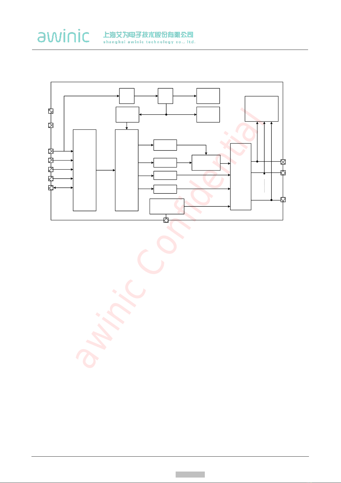
OPERATION MODE AND RESET
RESET
Power On Reset
Upon initial power-up, the AW21018 is reset by internal power-on-reset, and all registers are reset to default
value, and the chip is shut down.
Once the supply voltage VDD drops below the threshold voltage VPOR(2.0V), the power-on-reset will reset the
chip again. By reading the bit PUST of the register UVCR (address 60h), whether the chip has been reset can
be detected.
When the VDD ramps up above the threshold voltage VPOR (2.0V) and EN is high, POR is pulled high, meanwhile
the chip enters into initialization mode. The chip needs about 2ms to load the efuse information in initalization
mode. After initialization, it works in lower-power mode. About 200μs delay is required after CHIPEN is pulled
up, otherwise, internal OSCCLK may work incorrectly. Only in low-power and active mode, registers could be
configurated. The recommended operation timing is shown as bellow.
VDD
POR
CHIPEN
OSC
Initialization
initial
Standby Active
200μs
EN
..
2ms
Shutdown
INITIAL
MODE
Note: Thechip needsabout 2ms for
initalization after power on
(bit CHIPEN of GCR register)
Note: Recommend CHIPEN=1 after Initial
Note: OSC operates stable,which needs
200μs after CHIPEN=1
Internal registers are configurable
Configuring
Time
Figure 7 Power On Timing
Software Reset
By writing 00h to register RESET (address 70h) in active mode, the software reset is triggered. Then all
registers will be reset to the default value and the chip enters into initialization mode.
After the software reset command is input by I2C, it needs to wait at least 2ms before any other I2C commands
awinic Confidential
Downloaded From Oneyac.com

AW21018
Feb. 2022 V1.1
www.awinic.com 10 Copyright © 2020 SHANGHAI AWINIC TECHNOLOGY CO., LTD
are accepted.
CHIPEN
OSC
Initialization
initial
Standby Active
200us
..
2ms
Active
INITIAL
MODE
Note: The device need about 2ms for
initalization after power on
(bit CHIPEN of GCR register)
Note: Recommend CHIPEN=1 after Initial
Note: OSC operate stable need 200μs
after CHIPEN=1
Internal registers areconfigurable
Configuring
Time
Software
Reset
Figure 8 Software Reset Timing
OPERATING MODE
Shutdown mode
The AW21018 enters into shutdown mode automatically when EN is pulled to low. In this situation, I2C interface
is not accessible, all registers will be reset and can not be configured.
Initialization mode
If EN is high, AW21018 enters into initialization mode. During this period, all registers will be reset and chip
starts loading efuse information automatically.
Standby mode
After initialization, the AW21018 enters into standby mode when the bit CHIPEN of the register GCR (address
20h) is ‘0’, or UVLO is triggered in active mode. In this mode, only POR and I2C circuits work. I2C interface is
accessible, and all registers can be configured now.
Active mode
The AW21018 enters into active mode when EN is high and the bit CHIPEN of the register GCR (address 20h)
is ‘1’.
Power save mode
In active mode, when the bit APSE of the register GCR (address 20h) is set to “1”, the auto power-save function
is enabled. When all LEDs are switched off and the value of all registers BR00L~BR17H are 00h and write
00h to register UPDATE(address 45h) for more than 32 ms, AW21018 automatically enters into power saving
mode. In power save mode, most analog blocks are disabled to minimize power consumption, but the registers
retain the data and keep it available via I2C. Once writing a non-zero value into any register among
BR00L~BR17H, the chip exits power-save mode immediately.
Thermal shutdown
The AW21018 enters the thermal shutdown mode when the junction temperature exceeds 165°C (typical)
automatically. In this mode, all the LEDx outputs are shut down. If the junction temperature decreases below
140°C (typical), the AW21018 returns to active mode.
awinic Confidential
Downloaded From Oneyac.com

AW21018
Feb. 2022 V1.1
www.awinic.com 11 Copyright © 2020 SHANGHAI AWINIC TECHNOLOGY CO., LTD
Initialization
Standby
Active
Software reset
CHIPEN=1
EN = H
Active mode
CHIPEN=0
Shutdown EN = LFrom all modes
VDD power on
Thermal Shutdown
OTST=1
OTST=0
Power Save APSE=0 or
Write a non-zero value
to register BRx
APSE=1 &&
All LEDs off > 32ms
Figure 9 AW21018 operating mode transition
FEATURE DESCRIPTION
CURRENT SETTING
The average output current of LEDx (x=1~18) can be expressed by the following formula,
𝑰𝑶𝑼𝑻(𝒙) = 𝑰𝑴𝑨𝑿 ×𝑮𝑪𝑪
𝟐𝟓𝟓 ×𝑺𝑳𝒙
𝟐𝟓𝟓 ×𝑩𝑹𝒙
𝟐𝑷𝑾𝑴𝑹𝑬𝑺 𝒙 = 𝟏~𝟏𝟖
Where IMAX=40mA when REXT=4KΩ, GCC is the 8bit global current configured by the register GCCR (address
58h), SLx is 8bit individual constant current parameter configured by the register SLx (address 46h~57h) ,
PWMRES is 8bit/9bit/12bit PWM resolution configured by the register GCR (address 20h), and BRx is
8bit/9bit/12bit individual PWM modulated current parameter configured by the register BRxL/BRxH (address
21h~44h).
PWM MODLULATION
Dither Function
When PWMRES[1:0] of GCR(address 20h) equal to ‘11’, dither function is enabled. Then the final output PWM
has the frequency equal to 9 bits and resolution equal to 12 bits. This is achieved by 9 bits PWM modulation
and 3bits digital dither control. For 3-bit dither, every PWM in the 8 PWM group can be added one LSB or not
according to the 8-bit digital dither timing.
PWM Frequency
The output PWM frequency is decided by bits CLKFRQ [2:0] and PWMRES[1:0] in register GCR (address
20h). Following table shows the relationship of PWM frequency, the CLKFRQ [2:0] and PWMRES[1:0]. To
avoid the MLCC audible noise, it’s recommended to use the PWM frequency lower than 500Hz or higher than
20kHz.
BR Resolution
CLKFRQ[2:0]
000
001
010
011
100
101
110
111
awinic Confidential
Downloaded From Oneyac.com

AW21018
Feb. 2022 V1.1
www.awinic.com 12 Copyright © 2020 SHANGHAI AWINIC TECHNOLOGY CO., LTD
8bit
62k
32k
4k
2k
1k
500
244
122
9bit
32k
16k
2k
1k
488
244
122
-
12bit
4k
2k
244
122
-
-
-
-
9bit+3bit dither
32k
16k
2k
1k
488
244
122
-
.
PWM Phase Control
To reduce the peak load current and ceramic-capacitor audible ringing, AW21018 supports 6 PWM phase
shifting (Phase1~Phase6) and phase-inverting scheme. When setting PDE in register PHCR (address 59h) to
‘1’, the phase shifting scheme is enabled, and each adjacent phase differs by 60 degrees,which meaning
only 3 of 18 LEDs could switch on in the same time.
Phase1
LED1~LED3
Phase2
LED4~LED6
Phase3
LED7~LED9
Phase4
LED10~LED12
Phase5
LED13~LED15
Phase6
LED16~LED18
π/3
2π/3
3π/3
4π/3
5π/3
0
Figure 10 Phase shift scheme
When setting PINVTEn in register PHCR (address 59h, n=0~5) to ‘1’, the PWM phase of the even-numbered
channels is inverted. As shown below, if setting PINVTEn to ‘1’, the even-numbered channels are rotated 180
degrees counterclockwise when the odd-numbered channels are not, which is good for reducing the input-
current ripple. For an example, when setting PINVTE0 to ‘1’, LED2 is rotated 180 degrees counterclockwise
while the LED1 and LED3 are not.
PINVTE=“1”
PINVTE=“0”
LED[3n +1 ]
LED[3n +2 ]
n=0,2,4
LED[3n +3 ]
LED[3n +1 ]
LED[3n +2 ]
LED[3n +3 ]
awinic Confidential
Downloaded From Oneyac.com

AW21018
Feb. 2022 V1.1
www.awinic.com 13 Copyright © 2020 SHANGHAI AWINIC TECHNOLOGY CO., LTD
PINVTE=“1”
PINVTE=“0”
LED[3n +1 ]
LED[3n +2 ]
n=1,3,5
LED[3n +3 ]
LED[3n +1 ]
LED[3n +2 ]
LED[3n +3 ]
Figure 11 Phase invert scheme
PWM Disable
If the bits DCPWM [2:0] in register SSCR (address 5Fh) is set to “111”, the PWM output is disabled, and the
duty of each PWM is forced to 100%. In this mode, the BRx parameter is not valid, but the SLx parameter is
still effective.
It should be noted that when performing open-short detection, the bits DCPWM [2:0] need to be set to “111”.
GROUP CONTROL MODE
AW21018 supports group control mode, in this mode, all selected LEDs are controlled by the group control
registers (GSLR, GSLG, GSLB). The register GCFG select which LEDs are controlled by group control register.
There are total 6 control bits (GEx), each bit set adjacent 3 LEDs are included in or not. User can configure
group control register to setting common brightness and color for all selected LED, so as to simplify lighting
effect programming and speed up display refreshing via I2C interface.
If bit GSLDIS in register GCFG (address 8bh) is ‘1’, the color parameters of the grouped LED are no longer
configured by register GSLR/G/B but by individual register (SL0~SL15).
The detailed configurations are as follows.
LED
GE
Brightness
Color
GE=0
GE=1
GE=0 or
GSLDIS=1
GE=1 and
GSLDIS=0
1
GCFG[0]
BR00
GBR
SL00
GSLR
2
BR01
GBR
SL01
GSLG
3
BR02
GBR
SL02
GSLB
4
GCFG[1]
BR03
GBR
SL03
GSLR
5
BR04
GBR
SL04
GSLG
6
BR05
GBR
SL05
GSLB
…
…
…
…
…
…
13
GCFG[4]
BR12
GBR
SL12
GSLR
14
BR13
GBR
SL13
GSLG
15
BR14
GBR
SL14
GSLB
awinic Confidential
Downloaded From Oneyac.com

AW21018
Feb. 2022 V1.1
www.awinic.com 14 Copyright © 2020 SHANGHAI AWINIC TECHNOLOGY CO., LTD
16
GCFG[5]
BR15
GBR
SL15
GSLR
17
BR16
GBR
SL16
GSLG
18
BR17
GBR
SL17
GSLB
Note: GBR={GBRH,GBRL}.
SPREAD SPECTRUM
PWM is a troublesome for some application which is concerned about EMI. AW21018 has spread spectrum
function to optimize the EMI performance. If bit SSE in register SSCR (address 5Fh) is set to ‘1’, spread
spectrum function is enabled. By setting the bit SSR in register SSCR, four spread spectrum range
±5%/±15%/±25%/±35% can be selected. The total electromagnetic emitting energy can spread into a wider
range of frequency band that significantly degrades the peak energy of EMI.
RGB CONFIGURE MODE
In RGB applications, every 3 LEDs in RGB share a same BR parameter. To achieve fast register configuration
for RGB applications, AW21018 provides an RGB configuration mode by setting the bit RGBMD in register
GCR2 (address 61h).
If RGBMD=1, register BR00~BR05 configure brightness parameters for corresponding 6 RGB groups. In other
words, in RGB mode, only registers BR00~BR05 need to be configured, and the registers BR06~BR17 are
not valid any more.
If RGBMD=0, register BR00~BR17 configure brightness parameters for corresponding 18 LEDs independently,
more details as follows,
LED
BR parameter source
RGBMD=0
RGBMD=1
1
BR00
BR00
2
BR01
3
BR02
4
BR03
BR01
5
BR04
6
BR05
…
…
…
13
BR12
BR04
14
BR13
15
BR14
16
BR15
BR05
17
BR16
18
BR17
Note: BRxx = {BRxxH,BRxxL}
SINGLE BYTE CONFIGURATION MODE
By default, every LED has a 12bits BR parameter with BRxxL and BRxxH. The effective bit of BRxxH is 4bit.
However, AW21018 provides a single byte configuration mode by setting the bit SBMD in register GCR2
(address 61h). In single byte applications, every LED has a 8bit BR parameter configured by BR00L~BR08H.
awinic Confidential
Downloaded From Oneyac.com

AW21018
Feb. 2022 V1.1
www.awinic.com 15 Copyright © 2020 SHANGHAI AWINIC TECHNOLOGY CO., LTD
It is worth noting that the effective bit of BRxH(xx is 00~05) is 8 bit in single byte mode compared with default
mode.More details are as follows.
LED
BR parameter source
SBMD=0
SBMD=1
1
{BR00H,BR00L}
BR00L
2
{BR01H,BR01L}
BR00H
3
{BR02H,BR02L}
BR01L
4
{BR03H,BR03L}
BR01H
5
{BR04H,BR04L}
BR02L
6
{BR05H,BR05L}
BR02H
…
…
…
13
{BR12H,BR12L}
BR06L
14
{BR13H,BR13L}
BR06L
15
{BR14H,BR14L}
BR07L
16
{BR15H,BR15L}
BR07H
17
{BR16H,BR16L}
BR08L
18
{BR17H,BR17L}
BR08H
PATTERN CONTROLLERS
There is a breathing pattern controller in the chip. When bit PATE in register PATCFG (address 80h) is set to
‘1’, breathing pattern controller is enabled. Pattern controller can be configured as autonomous breathing mode
or manual-controlled mode. When corresponding GE is configured as ‘1’, if in pattern controlled mode, each
led group (consisting of three adjacent LEDs) can enter into breathing mode. When GE is ‘0’, the three adjacent
LEDs exit breathing mode directly. For example, when setting GCFG = 0x01 and in pattern controlled mode,
LED1~LED3 will work in breathing mode and other LEDs will work in default mode.
Autonomous Breathing Mode
When bit PATE and PATMD in register PATCFG are set to ‘1’, the pattern controller works in autonomous
breathing mode. In this mode, the pattern controller will generate a breathing lighting effect, which is configured
by the user-defined timing parameter. The waveform of the breathing lighting effect is shown in the following
figure. The parameter T0~T3 define 4 key periods in a complete breathing cycle. T0~T3 composite a breathing
loop, denoting the rise-time, on-time, fall-time and off-time respectively. Register GBRH (address 86h) and
GBRL (address 87h) control the max and min brightness of the breathing respectively.
T0 T1 T2 T3
GBRH
GBRL
Figure 12 LED breath timing in pattern mode
The start point and end point of autonomous breathing loop are configurable. The loop starting point could be
selected among T0~T3, which is set by bits LB [1:0] in register PATT2 (address 84h). The end point of the loop
can only be selected between the end of T3 and the end of T1, which is determined by bits LE [1:0] in register
awinic Confidential
Downloaded From Oneyac.com

AW21018
Feb. 2022 V1.1
www.awinic.com 16 Copyright © 2020 SHANGHAI AWINIC TECHNOLOGY CO., LTD
PATT2. If bits LE [1:0] is not “00”, the end point of breathing loop is the end of T1, and the loop counter
increment by 1 at the end of T1. If bit LE [1:0] is “00”, the loop end point is the end of T3, and the loop counter
increment by 1 at the end of T3.
The repeat times is decided by bit RPT [11:8] of register PATT2 (address 84h) and RPT [7:0] of register PATT3
(address 85h). When setting RPT [11:0] to ‘0’, the breathing pattern will run unlimited times.
After the breathing pattern is over, the status bit PATIS in register PATGO (address 81h) will be set to ‘1’, and
PATIS will be cleared to ‘0’ after reading out through I2C bus. Once breathing loop start again or pattern
controller switches to manual mode by setting PATE bit to ‘0’, the PATIS will also be cleared.
When bit RUN in register PATGO is set to ‘1’, breathing pattern is started. The full process of the autonomous
breathing is as follows:
1. Set GSLR/G/B, GBRH/L parameter.
2. Set GCFG to select the LED in breathing pattern mode or not.
3. Configure PATT0, PATT1, PATT2, and PATT3 for parameters T0~T3, start/stop point, and repeat
times.
4. Set PATE=1 to enable breathing pattern mode.
5. Set PATMD=1 to select auto breathing mode.
6. Set RUN=1 to start the breath pattern.
Manual Control Mode
If bit PATMD is set to ‘0’, manual control mode is selected. In manual control mode, user could program the bit
SWITCH of register PATCFG to control the output of pattern controller. When bit SWITCH is ‘1’, the output of
pattern controller is decided by register GBRH. When bit SWITCH is set as “0”, the output is the decided by
register GBRL.
If bit RAMPE in register PATCFG is set to ‘1’, the smooth ramp up/down will be enabled. At the same time, if
SWITCH changes from “0” to ‘1’, the output will be ramp up to GBRH smoothly. Similarly, if SWITCH changes
from “1” to ‘0’, the output of the pattern controller will ramp down to GBRL smoothly.
However, if the RAMPE is set to ‘0’, the output of the pattern controller will change to GBRH or GBR directly
with no ramp as the SWITCH changes.
Set PATCFG.SWITCH =1
fade-in fade-out
PATCFG.RAMPE =0
PATCFG.RAMPE =1
Set PATCFG.SWITCH =0
GBRH
GBRL
GBRH
GBRL
Figure 13 Manual Control Mode
PROTECTION FEATURES
Under Voltage Lock Out (UVLO)
When bit UVDIS of the register UVCR (address 60h) is set to ‘0’, the chip monitors the voltage of VDD. If the
supply voltage drops below threshold (2.5V typically), the bit UVST of the register UVCR (address 60h) will be
set to ‘1’. After read-out, the register UVCR will be clear.
If both bit UVDIS and bit UVPD of the register UVCR (address 60h) is set to ‘0’, UVLO protection function is
enabled. Once the event of under voltage occurs, the bit CHIPEN of the register GCR (address 20h) will be
awinic Confidential
Downloaded From Oneyac.com

AW21018
Feb. 2022 V1.1
www.awinic.com 17 Copyright © 2020 SHANGHAI AWINIC TECHNOLOGY CO., LTD
cleared to ‘0’, and then the chip will enter into standby mode. If the voltage of VDD rises above 2.6V then write
“1” to bit CHIPEN, the chip will enter into active mode again.
By default, control bits UVDIS, UVPD are all “0”. Both UVLO monitor and protection are enabled.
Over Temperature Protection (OTP)
When bit OTDIS of the register OTCR (address 5Eh) is set to ‘0’, the over-temperature detection is enabled.
Once the temperature of this chip reaches 165°C, the over-temperature condition is detected, and the bit OTST
of the register OTCR (address 5Eh) will be set to ‘1’. The OTST will be cleared to ‘0’ after reading the register
OTCR.
If both bit OTDIS and bit OTPD of the register OTCR (address 5Eh) are set to ‘0’, the Over-Temperature
Protection (OTP) function is enabled. Once the temperature is over 165°C, the bit CHIPEN of the register GCR
(address 20h) will be cleared to ‘0’, and then the chip will enter into thermal shutdown mode. When the
temperature returns below 140°C, the chip will enter into active mode again after writing “1” to bit CHIPEN.
By default, control bits OTDIS and OTPD are all “0”, both OT monitor and OT protection are enable.
LED Open/Short Detection
AW21018 supports LED open/short detection. When bit OSDE[1:0] of the register OSDCR(address 5Ah) is
set to “10” , short detection is enabled, and the detection results can be read out via the registers
OSST0~2(5Bh~5Dh). Similarly, when set bit OSDE [1:0] of the register OSDCR (address 5Ah) to “11”, open
detection is enabled, and the results also can be read out via the registers OSST0~2.
The valid detect result is determined by:
⚫Short Detection: VLED > VDD- VTHSHORT
⚫Open Detection: VLED < VTHOPEN
Where VTHOPEN: Threshold of open detection (When OTH=0, VTHOPEN = 0.1V,else VTHOPEN = 0.2V;).
VTHSHORT: Threshold of short detection (When STH=0, VTHSHORT = 0.5V,else VTHSHORT = 1V).
VLED:The voltage of chip LED pin.
We recommend the bit DCPWM[2:0] of the register SSCR (address 5Fh) being set to “111” and maintain about
1mA current of each LED when the open/short function is enabled.
awinic Confidential
Downloaded From Oneyac.com

AW21018
Feb. 2022 V1.1
www.awinic.com 18 Copyright © 2020 SHANGHAI AWINIC TECHNOLOGY CO., LTD
I2C INTERFACE
The AW21018 supports the I2C protocol. The maximum frequency supported by the I2C is 1 MHz. The pull-up
resistor for the SDA and SCL can be selected from 1k to 10kΩ. Usually, 4.7kΩ is recommended for 400 kHz
I2C, 1kΩ is recommended for 1 MHz I2C. The voltage from 1.8V to 3.3V is allowed for the I2C interface.
Additionally, the I2C chip supports continuous read and write operations. Particularly, if register address is
00h or 01h, the slave chip will poll register address between 00h and 01h.
CHIP ADDRESS
The I2C chip address is 7-bit (A7~A1), followed by the bit R/W (A0). Set A0 to “0” for writing and “1” for reading.
The values of bit A1 and A2 are depended on the pin AD0. A3 and A4 are depended on the pin AD1. There are
2 options: VDD and GND. The A7 to A5 is “010” constantly. The chip also supports using a broadcast slave
address of 1Ch. All slave addresses as followed.
AD PIN
A7:A5
A4:A3
A2:A1
A0
Chip Address
Broadcast Address
GND/GND
010
00
00
0/1
20h
1Ch
GND/VDD
00
01
21h
VDD/GND
01
00
24h
VDD/VDD
01
01
25h
I2C START/STOP
All transactions begin with a START and are terminated by a STOP sent by master to slave. A high-to-low
transition on the SDA input/output while the SCL input is high defines a START condition. A low-to-high
transition on the SDA input/output while the SCL input is high defines a STOP condition.
In particular, the bus stays busy when a repeated START (Sr) is generated instead of a STOP signal
corresponding to the lastest START (S). Sr and S are usually regarded as equivalent.
SCL
SDA
S/Sr
S: START condition
Sr: START Repeated condition P: STOP condition
P
Figure 14 I2C START/STOP Condition Timing
DATA VALIDATION
When SCL is high level, SDA level must be constant. SDA can be changed only when SCL is low level.Each
SCL pulse corresponds to one bit data transaction.
awinic Confidential
Downloaded From Oneyac.com

AW21018
Feb. 2022 V1.1
www.awinic.com 19 Copyright © 2020 SHANGHAI AWINIC TECHNOLOGY CO., LTD
SCL
SDA
Data Line
Stable
Data Valid
Change
of Data
Allowed
Figure 15 Data Validation Diagram
ACK (ACKNOWLEDGEMENT)
ACK means the successful transaction of I2C bus data. During writing cycle, after master sends 8-bit data,
SDA must be released by master and SDA is pulled down to GND by slave chip when slave sends ACK.
During reading cycle, after slave chip sends 8-bit data, slave releases the SDA and waits for ACK from master.
If master sends ACK with STOP condition, slave chip sends the next data. If master sends NACK, slave chip
stops sending data and waits for I2C stop.
12 8 9
Data Output
by Transmitter
DataOutput
by Receiver
SCL From
Master START
condition
Not Acknowledge(NACK)
Acknowledge(ACK)
Clock Pulse for
Acknowledgement
Figure 16 I2C ACK Timing
WRITE CYCLE
One data bit is transferred during each clock pulse. Data is sampled during the high state of the serial clock
(SCL). Consequently, throughout the clock’s high period, the data should remain stable. Any changes on the
SDA line aborts the current transaction during the high state of the SCL. New data should be sent to SDA bus
during the low SCL state. This protocol allows a single data line to transfer both command/control information
and data using the synchronous serial clock.
Each data transaction is composed of a start condition, a number of byte transfers and a stop condition to
terminate the transaction. Every byte written to the SDA bus must be 8 bits and is transferred with the most
significant bit first. After each byte, an Ack signal must follow.
1. In a write process, the following steps should be followed:
2. Master chip generates START condition. The “START” signal is generated by pulling down the SDA
signal while the SCL signal is high.
3. Master chip sends slave address (7-bit) and the data direction bit R/𝑊
= 0.
4. Slave chip sends acknowledge signal if the slave address is correct.
5. Master sends control register address (8-bit).
6. Slave sends acknowledge signal.
7. Master sends data byte to write to the addressed register.
awinic Confidential
Downloaded From Oneyac.com

AW21018
Feb. 2022 V1.1
www.awinic.com 20 Copyright © 2020 SHANGHAI AWINIC TECHNOLOGY CO., LTD
8. Slave sends acknowledge signal.
9. If master send more data bytes, the control register address will be incremented by one after
acknowledge signal (repeat step f and g).
10. Master generates STOP condition to indicate write cycle ends.
0
A2 A1 A0A6 A5 A3A4 A4 A3 A1A2A7 A5A6
123456780123456
D5 D4 D2D3A0 D6D7 D1 D0
78012345678SCL
SDA Ack
Ack
Start
R/W
Stop
Device Address Register Address Write Data
Ack
Figure 17 I2C Write Byte Cycle
READ CYCLE
In a read cycle, the following steps should be followed:
1. Master chip generates START condition
2. Master chip sends slave address (7-bit) and the data direction bit (R/W = 0).
3. Slave chip sends acknowledge signal if the slave address is correct.
4. Master sends control register address (8-bit)
5. Slave sends acknowledge signal
6. Master generates STOP condition followed with START condition or REPEAT START condition
7. Master chip sends slave address (7-bit) and the data direction bit (R/W = 1).
8. Slave chip sends acknowledge signal if the slave address is correct.
9. Slave sends data byte from addressed register.
10. If the master chip sends acknowledge signal, the slave chip will increase the control register address by
one, then send the next data from the new addressed register. In particular, if register address is 00h or
01h, the slave chip will poll register address between 00h and 01h.
11. If the master chip generates STOP condition, the read cycle ends.
0
A2 A1 A0A6 A5 A3A4 A4 A3 A1A2A7 A5A6
123456780123456
A4 A3 A1A2
A0
A5A6 D6 D0D1A0 D7
7
01234567801... 6
SCL
SDA Ack
Ack
Ack
7 8
Ack
start
R/W
……
stop
Device Address Register Address
Device Address Read Data
8
RS
Using
Repeat start
A4 A3 A1A2A5A6 D6 D0D1A0 D7
0 1 2 3 4 5 6 7 8 0 1... 6
Ack
7 8
Ack
……
stopReadData
S
Separated
Read/write
transaction
……
……
Device Address
P
……
…… R/W
R/W
Figure 18 I2C Read Byte Cycle
awinic Confidential
Downloaded From Oneyac.com
This manual suits for next models
1
Table of contents