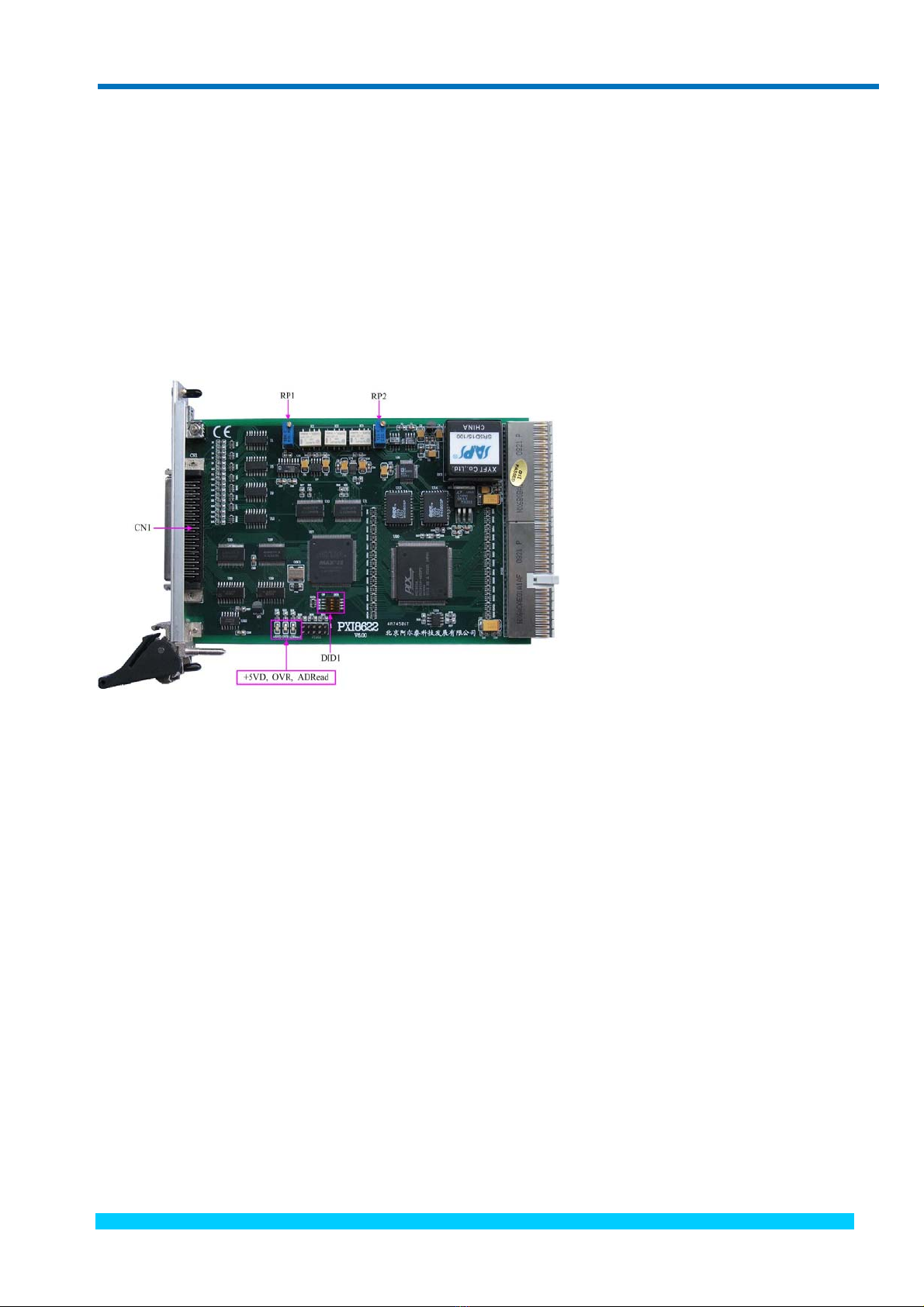
PXI8622 Data Acquisition V6.0.15
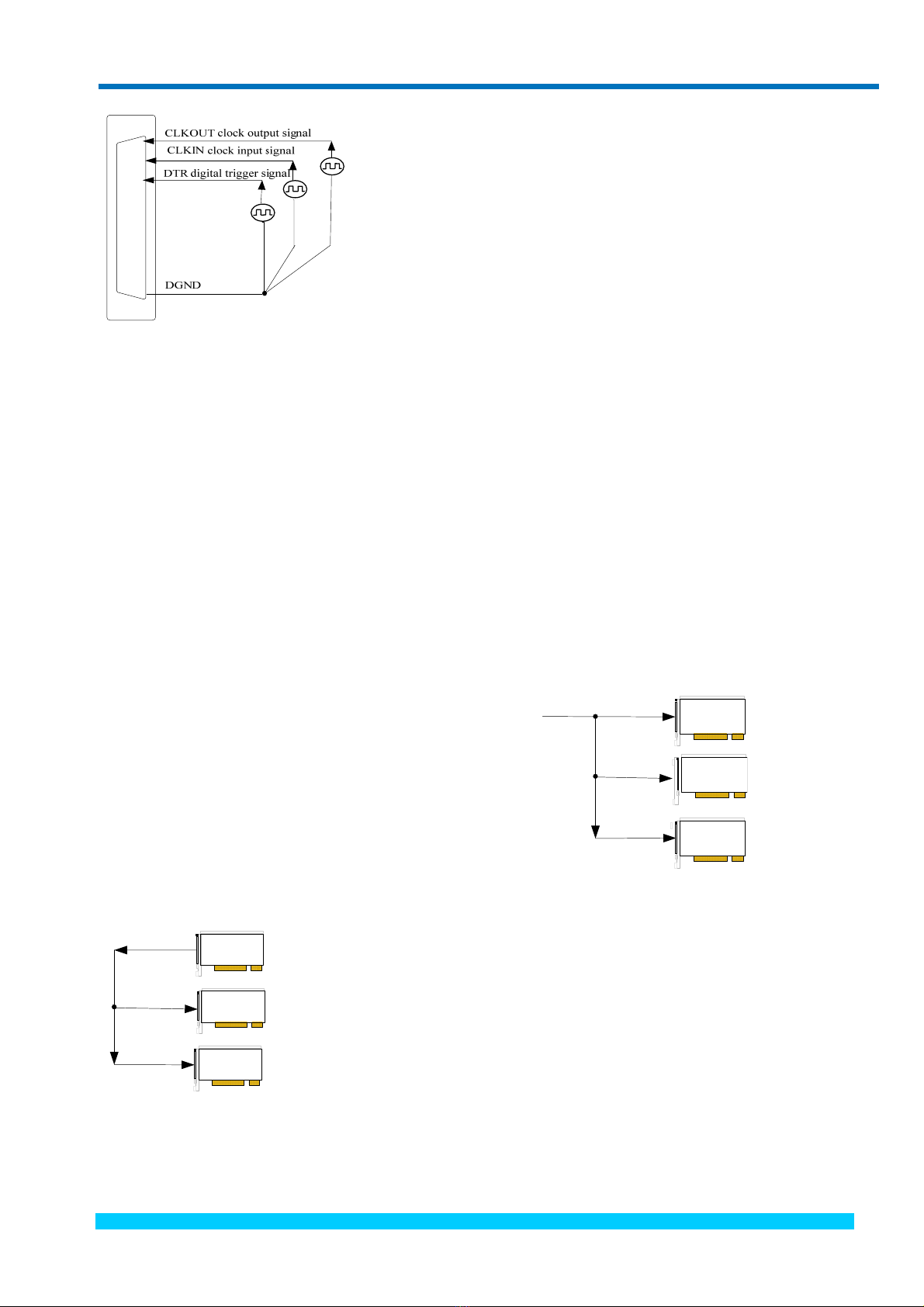
Figure 4.2.3 clock input / output and trigger signal connection
4.4 Methods of Realizing the Multi-card Synchronization
Three methods can realize the synchronization for the
PXI8622, the first method is using the cascade
master-slave card, the second one is using the common
external trigger, and the last one is using the common
external clock.
When using master-slave cascade card programs, the
master card generally uses the internal clock source
model, while the slave card uses the external clock
source mode. After the master card and the slave card are
initialized according to the corresponding clock source
mode. At first, start all the slave cards, as the main card
has not been activated and there is no output clock signal,
so the slave card enters the wait state until the main card
was activated. At this moment, the multi-card
synchronization has been realized. When you need to
sample more than channels of a card, you could consider
using the multi-card cascaded model to expand the
number of channels.
Slave Card 2
CLKOUT
CLKIN
CLKIN Slave Card 1
Master Card
When using the common external trigger, please make
sure all parameters of different PXI8622 are the same. At
first, configure hardware parameters, and use analog or
digital signal triggering (ATR or DTR), then connect the
signal that will be sampled by PXI8622, input triggering
signal from ART pin or DTR pin, then click “Start
Sampling” button, at this time, PXI8622 does not sample
any signal but waits for external trigger signal. When
each module is waiting for external trigger signal, use
the common external trigger signal to startup modules, at
last, we can realize synchronization data acquisition in
this way. See the following figure:
PXI8622
External Trigger Signal
DTR
DTR
DTR PXI8622
PXI8622
Note: when using the DTR, use the internal clock mode
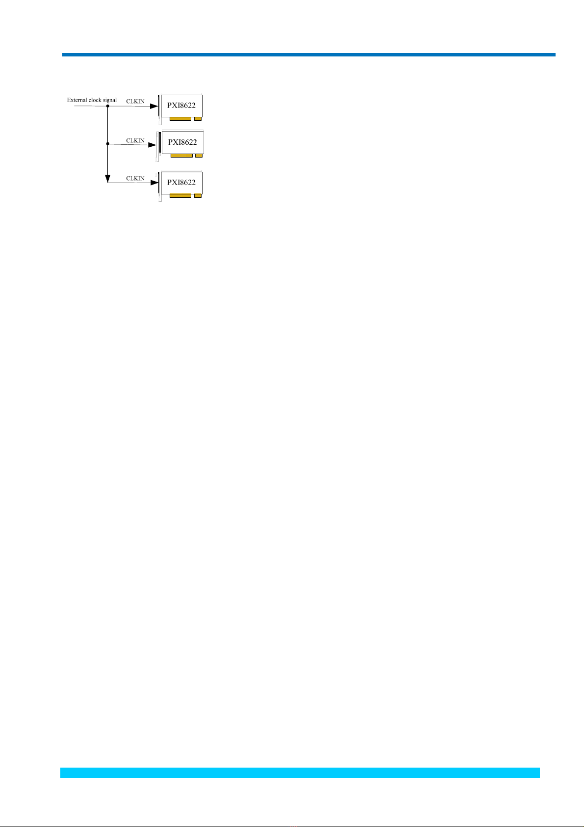
When using the common external clock trigger, please
make sure all parameters of different PXI8622 are the
same. At first, configure hardware parameters, and use
external clock, then connect the signal that will be
sampled by PXI8622, input trigger signal from ART pin
or DTR pin, then click “Start Sampling” button, at this
time, PXI8622 does not sample any signal, but wait for
external clock signal. When each module is waiting for
external clock signal, use the common external clock
signal to startup modules, at last, we realize
synchronization data acquisition in this way. See the
BUY ONLINE at art-control.com/englishs or CALL+86-10-64862359/64861583(CN) 9