manuals.online logo
Brands
  1. Home
  2. •
  3. Brands
  4. •
  5. BHI
  6. •
  7. Control Unit
  8. •
  9. BHI NEDSP1901-PCB-MIC User manual

BHI NEDSP1901-PCB-MIC User manual

Page 1
bhi
Copyright & Disclaimer:
Copyright: This publication, including all photographs and illustrations is protected under
international copyright laws, with all rights reserved. Neither this manual, nor any of the material
within, may be copied or reproduced without the written consent of bhi Ltd.
Disclaimer: The information in this document is subject to change without notice. bhi Ltd. makes no
representations or warranties with respect to the contents hereof and specifically disclaims any
implied warranties of merchantability or fitness for any particular purpose. Furthermore, bhi Ltd.
reserves the right to revise this publication and to make changes from time to time in the content
hereof without obligation of bhi Ltd. to notify any person of such revision or changes.
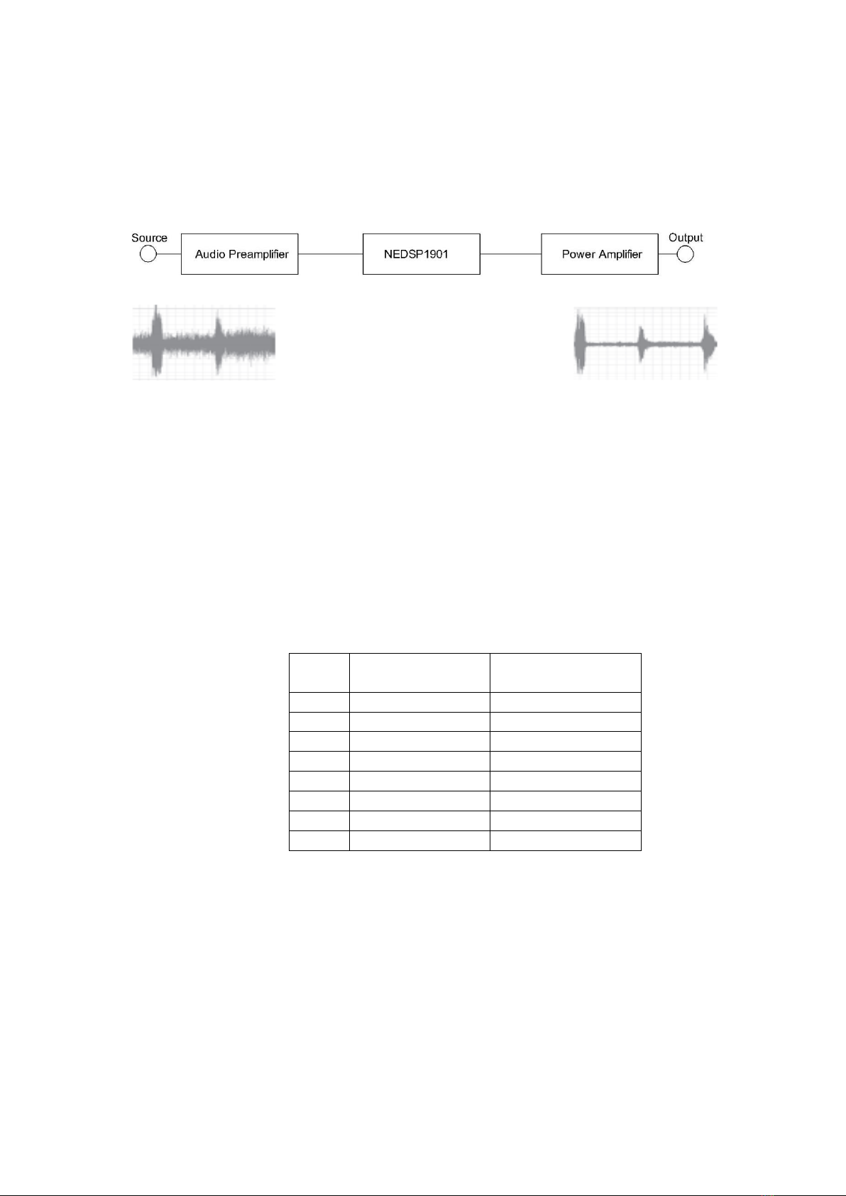
1. Introduction –The NEDSP1901-PCB module is designed to take line level audio signals and
the NEDSP1901-PCB-MIC version is designed for use with various microphones. They are
separate products and need to be ordered separately, and they are not interchangeable,
although the NEDSP1901-PCB-MIC can also be used with line level audio signals.
Note: Go to page 12 for the specific NEDSP1901-PCB-MIC information
NEDSP1901-PCB Version:
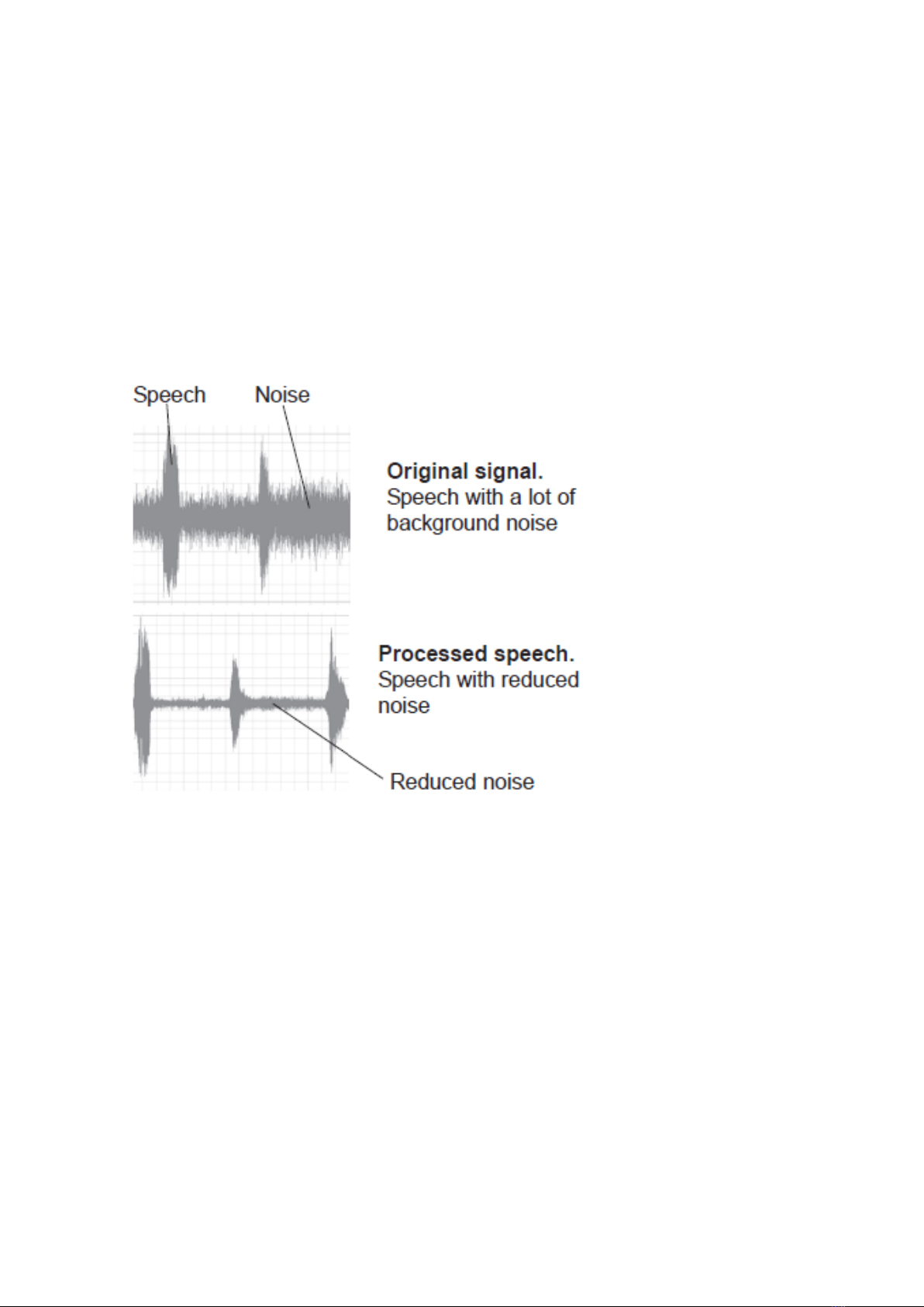
The NEDSP1901-PCB module is an audio DSP noise cancelling module that is used to clean up noisy
speech signals to give improved speech clarity in noisy conditions. The 1901 module is pin for pin
replacement module for the discontinued NEDSP1061-PCB module. It operates with a similar
specification but incorporates the latest bhi DSP noise cancelling technology and maintains virtually
the same physical dimensions as the NEDSP1061-PCB.
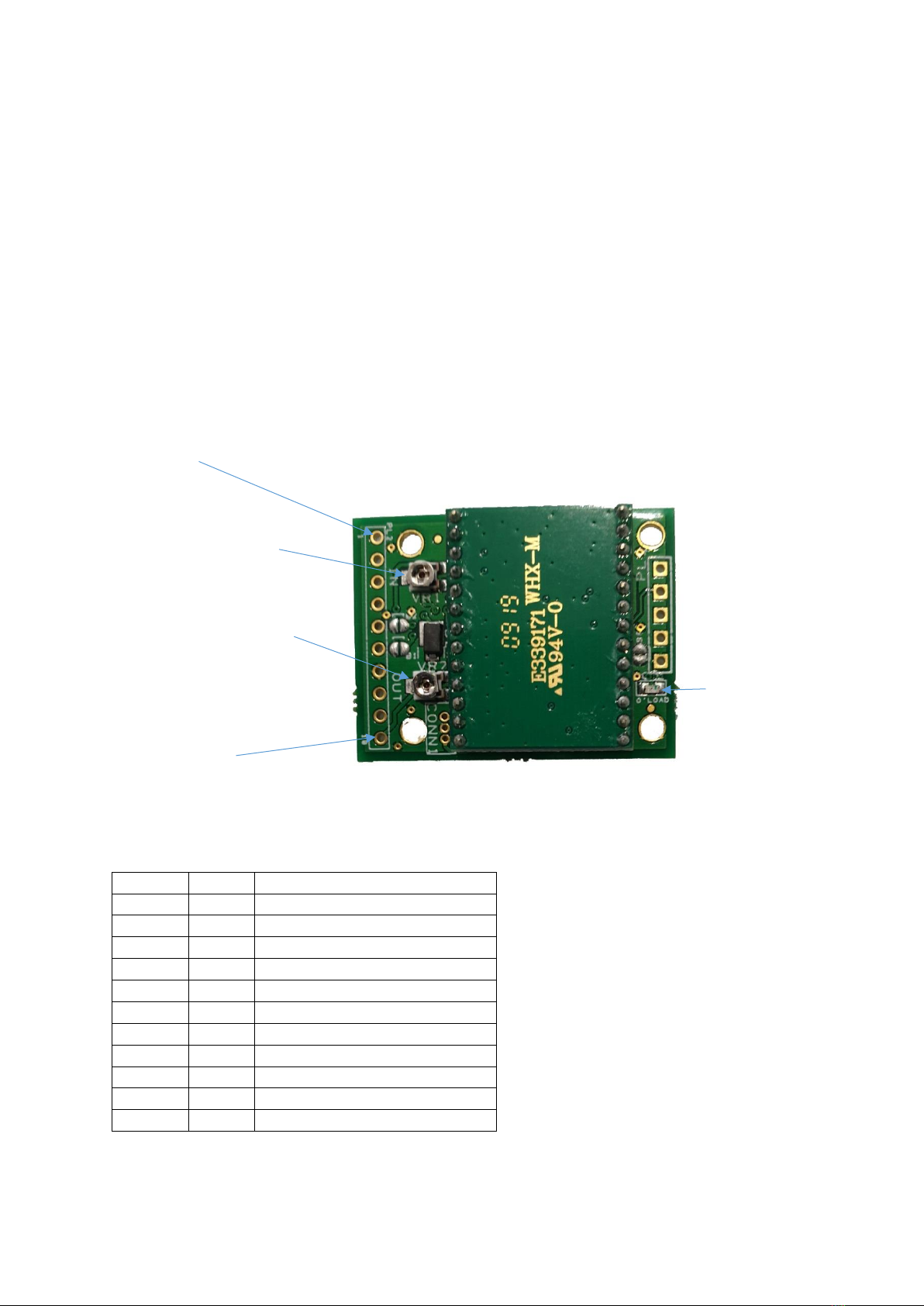
DSP side of PCB Rear side of PCB
1.1 NEDSP 1901 Module Features:
•Fully adaptive to changing noise environments
•Input and output level controls
•Virtually no distortion to speech signals
•Up to 40 dB noise reduction in 8 selectable levels
•Audio bandwidth 300Hz to 5KHz
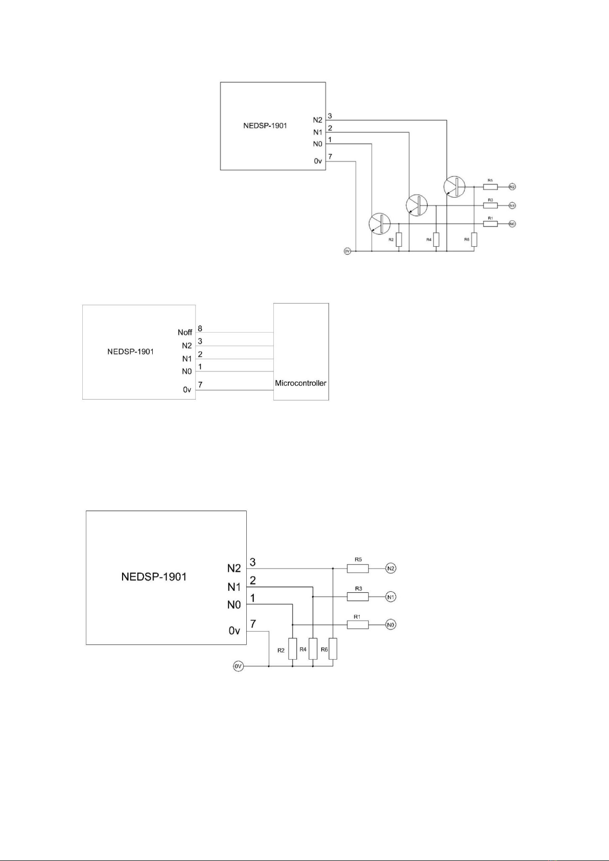
•Noise Reduction may be preset or remotely set during operation.
•7 to 18 Volt supply range
•Approximately 10 dB of signal gain with the ability to drive impedances of less than 1KOhm.
•Wide range of connection possibilities
•Mounting holes
NEDSP1901-PCB User Manual Iss A
NEDSP1901-PCB-MIC User Manual Iss A
www.bhi-ltd.com
Page 2
1.2 Limitations
This module is designed to pass speech. Other signals such as data, music and morse (CW) will, to
some degree pass through, but the integrity of these signals cannot be guaranteed. Like the
NEDSP1061-PCB module it is designed to be placed in a low-level audio path (up to 1V p-p) only,
although there is a level adjustment on the module which will require adjustment. The output will
not drive a loudspeaker or other high-power load.
1.3 Module connection and Mounting
Connections to the module are made by a row of 10 plated through holes to one end which form
PL2. The holes are on a 2.54 mm (0.1”) pitch which allow the use of Straight or Right-angle pin
headers or direct wiring. This makes a flexible connection arrangement and allows the using to be
mounted either vertically or horizontally, plugged in or soldered directly to the target system.
PL1, seen on the right of the picture above,
is meant for programming of the 1901-KBD
module only.
Connections to the 1901 are via PL2, as
given in the table opposite.
Whichever method of connection is used, ensure that the PCB is supported by using at least 2 of the
Pin No
Name
Description
1
N0
BCD lsb noise reduction bit 0
2
N1
BCD noise reduction bit 1
3
N2
BCD msb noise reduction bit 2
4
N/C
Do Not Connect
5
Vin
Vin Supply Voltage (5V to 20 V)
6
N/C
Do Not Connect
7
0v
0V connection
8
Noff
Noise Reduction On/Off pin
9
In
Audio Input
10
Out
Audio Output
PL2 pin 1
Input Level adjustment
Output Level adjustment
PL2 pin 10
Overload
LED
Page 3
M2.5 mounting holes to be found at the corners of the board. It’s recommended that Nylon
Securing hardware is used to ensure that accidental shorts are avoided due to the fine nature of this
PCB. The Audio signal into the module is capacitor coupled to prevent DC offsets being affected.
An on-board voltage regulator allows the module to be used with a wide range of input voltages, but
to keep the power dissipation (and heat) down, it is advisable to use as low as possible supply
voltage. The power supply input is reverse polarity protected.
1.4 DSP Noise Reduction
The NEDSP1901 processes the incoming signal and uses known speech and noise patterns to
differentiate the speech from the noise. The unwanted noise and interference is then attenuated to
leave only speech.
The module has the facility
to be pre-set or adjusted
during operation. Digital
inputs control the functions.
These incorporate internal
pull-up resistors so they can
be left floating when not in
use.
The diagrams in Figure 1
(opposite) are taken from
actual audio signals and
illustrate how the signal is
being processed.
Figure 1 –Noise Cancellation
Page 4
2.0 Module Description
2.1 Block Diagram
The NEDSP 1901 module has the facility to be preset or adjusted during operation. Digital input
control the functions. These incorporate internal pull-up resistors so they can be left floating when
not in use.
The audio signals into and out of the module are capacitor coupled to ensure that no DC levels are
pulled down or shorted when the module is used embodied as part of existing equipment.
The on-board voltage regulator allows the module to operate from a wide supply voltage (5 to 15
Volts) range. However, to keep the power dissipation (heat) down, it is advisable to use as low as
possible supply voltage. The Power supply input is reverse polarity protected.
Figure 2. NEDSP1901 Block Diagram
Page 5
2.2 Module Layout
Figure 3 below shows the board dimension detail as seen from above. The overall thickness of the
board is 8.75mm. When considering the installation of this module, at least 9.5 mm height should be
provided, which will allow for the clearance of through-hole solder pins.
Figure 3. Board outline dimensions and mounting hole positions
The Jumpers NS0 through NS2 highlighted in Figure 4 are solder jumper pads to allow the user to fix
the Nosie Reduction level required. Care must be taken so as not to splash solder over un-used
solder pads when placing solder across the required jumpers.
Note: Ensure that any solder jumpers across these pads are removed before using the Remote Noise
Reduction control pins.
Figure 4. On-board Noise Reduction level selection jumpers
N0 solder
pad jumper
N1 solder
pad jumper
N2 solder
pad jumper
Page 6
2.3 Pin Functions
The basic operation of the NEDSP pins is described below. More details may be found later in this
manual.
Pins 1-3 DSP Filter level set -These pins allow remote setting of the noise cancellation level. If these
pins are used, then ensure that the appropriate on-board pre-set solder jumpers are
removed (JP1 –JP3).
Pin 5 Supply Voltage - Supply voltage 5 V to 15 V DC
Pin 7 0V - This is the 0V pin and acts as a Star Point for all Audio and Power Grounds.
Pin 8 Noise Reduction On/Off - Connecting this pin to 0V inhibits the noise cancellation. Leave
this pin floating or tie it to +3.3 V to enable noise cancellation.
Pin 9 Audio Input - Audio Signal to be processed
Pin 10 Audio Output - DSP Processed signal from the module.
For optimum performance, keep all leads as short as possible. Use screened leads for the audio
signal and make sure that the 0V pin is grounded correctly with all signal grounds being reference to
this pin.
2.4 Controls
The audio level control potentiometers VR2 (Audio Out) and VR1 (Audio In) provide adjustment to
audio levels entering and leaving the module. Both controls are pre-set at the factory such that a 1V
p-p input provides a 1V p-p output with the Noise Reduction disabled.
To set the Input Level correctly, adjust VR1 until the ‘Overload’ indicator (LED1) just illuminates.
Then back off the potentiometer until the LED extinguishes. Turning the potentiometers clockwise
increases the levels.
2.5 Electrical Characteristics
Output impedance: 1k Ohms typical
Input impedance: 7.5k Ohms typical
Analogue Characteristics
Parameter
Description
Min.
Typ.
Max.
Units
Vin
Supply Voltage
5
8
15
V
Iin
Supply Current
15
20
mA
In
Audio Input Signal
10
500
mV (rms)
Out
Audio Output Signal
1000
Digital Characteristics
Parameter
Description
Min.
Typ.
Max.
Units
VHigh
High Level Input Voltage
-
3.3
5
V
VLow
Low level Input Voltage
0.8
-
-
V
Page 7
3.0 Installation
The NEDSP1901 module is inserted into the path of the noisy audio. Adjusting the Input and Output
level controls allows the module to appear transparent to the audio signal level.
Figure5. General Audio signal flow with 1901 module installed
The NEDSP1901 requires a minimum signal level of 10mV rms or greater for optimum performance.
Signals lower than this may be used but the noise cancellation performance will be degraded as the
signal level drops. If the module is to be used with low level microphones, the signal will require
pre-amplification. The Output level control may be used to attenuate the signal back down to the
original signal level.
4.0 Functions
4.1 Noise Reduction Levels
8 Levels of noise reduction are available. Noise and tone reduction is shown in the table below:
Notes:
1. When processing signals with high levels of noise using the higher levels of Noise reduction,
the processed signal may sound a little strange. This quite normal with this type of signal.
2. Due to the adaptive nature of the noise cancellation algorithm, a small delay may be
experienced when the audio signal varies in the noise. For optimum performance the
module should be provided with a constant signal, for example if the module is installed into
a system employing a push to talk system, then the module should be inserted in the audio
path before any switching or muting. Thus, the signal will always be available for the
module to adapt to.
Level
Tone Reduction
White Noise
Reduction
1
4dB
8dB
2
5dB
12dB
3
6dB
16dB
4
8dB
20dB
5
16dB
25dB
6
21dB
30dB
7
25dB
35dB
8
65dB
40dB
Page 8
4.2 Setting different filter levels
The levels are set by applying a BCD code to three solder jumpers on the underside of the module.
The module can be controlled with a microcontroller. As the DSP employs internal pull-ups, it is not
necessary to drive the microcontroller pins high, they can be placed in a high impedance state.
4.3 Remote setting of DSP filter level
Remote setting of the DSP level may be achieved through the PCB connections at PL2, this allows the
filter level to be changed during operation. If the remote DSP settings are to be used, ensure that
the solder jumpers are removed from NS0 through NS2 as shown below:
To set the DSP level remotely, connect the pins N0, N1 and N2 (PL2 pins 1, 2 and 3 respectively) as
shown in Table 2 below. The DSP Module has internal pull-ups on its inputs, so any cell in the table
containing +3.3 V may be taken up to or left open circuit.
Level
N2
N1
N0
1
0 V
0 V
0 V
2
0 V
0 V
+3.3 V
3
0 V
+3.3 V
0 V
4
0 V
+3.3 V
+3.3 V
5
+3.3 V
0 V
0 V
6
+3.3 V
0 V
+3.3 V
7
+3.3 V
+3.3 V
0 V
8
+3.3 V
+3.3 V
+3.3 V
Table 2 –Remote Pin settings for various Noise Reduction Levels
4.4 Setting the Noise Reduction Level using the On-board Jumper links
The on-board Noise reduction selection jumper selectors are located on the underside of the
Module as shown below. These jumpers are actually PCB pads that should be linked using a solder
bridge. Caution should be used when carrying out this operation to ensure that other components
and connections are not bridged as this could cause the module to malfunction or even fail.
The Noise reduction Level settings
are shown in the table below.
Table 3 –On-board Jumper setting
Level
NS2
NS1
NS0
1
Open
Open
Open
2
Open
Open
Linked
3
Open
Linked
Open
4
Open
Linked
Linked
5
Linked
Open
Open
6
Linked
Open
Linked
7
Linked
Linked
Open
8
Linked
Linked
Linked
NS0
NS1
NS2
Page 9
4.5 Noise Reduction On/Off
The module has the provision for remotely enabling and disabling the noise reduction, while in
operation. The default setting for the module is noise reduction ON. This may be switched by the use
of the noise cancellation On/Off pin (PL2 pin 8). To inhibit noise reduction, connect this pin to 0V. To
enable the noise reduction, leave the pin unconnected.
The module may be controlled with a microprocessor. As the 1901 Module employs internal pull-
ups, it is not necessary to drive the microprocessor port pins high, they can be placed in a high
impedance state.
It should be noted that the 1901 module operates with 3.3 Volt logic signals. Therefore, if it is
intended that the Microprocessor is to drive the 1901 lines High, the Microprocessor should be
operating from a 3.3 Volt supply as well. Alternatively, the control signals may be attenuated using a
simple potential divider as discussed in section 5.
5. Application Notes
5.1 Noise Cancellation On/Off with indication
In the example opposite a
Tricolour (or separate Red and
Green) LED’s are used to give a
visual indication of the Noise
Reduction mode. The Green
LED will illuminate when the
Noise Reduction is On and the
Red will illuminate when the
Noise Reduction is Off.
Figure 7. Noise Reduction On/Off with Red/Green LED Status indicator
5.2 Remote adjustment of Noise Reduction level
This section illustrates the various options for altering the DSP level remotely, during operation.
Figure 8. Basic setting using a BCD switch with complementary logic.
Page 10
The transistors allow
interfacing with higher
voltages to control the DSP
level. As a rough guide the
Resistors R1, R3, R5 can be
around 10 kOhm. Resistors
R2, R4 and R6 could be in
the range 2.2 kOhm for
control voltages over 10
Volts and 4.7 kOhm for
voltages between 5 Volts
and 10 Volts.
Figure 9. Noise Reduction setting using a Transistors
The module can be controlled with a
microcontroller. It is not necessary to
drive the control pins with the controller
as the NEDSP has internal pull-up
resistors. Therefore, the microcontroller
would operate pulling Low or in a High
impedance state.
Figure 10 –Operation with a Microcontroller
Important Note: If the Microcontroller is driving the control pins both High and Low, it should be
operate from a 3.3 Volt supply only. If this can’t be achieved, then consider using either the
Transistor method of interfacing above or the much simpler voltage divider method outlines for 5
Volt operation shown in Figure 11.
If a Microcontroller
operating on 5 Volts is to
be used to drive the
NEDSP1901 control pins,
make sure that the drive
voltage is no higher than
3.3 Volts. Alternatively, if
the Microcontroller is
operating on 5 Volts,
insert a simple Voltage
divider circuit between
the control pins and the
microcontroller.
Figure 11. Alternative method of controlling the NEDSP1901 with 5 Volt logic.
For +5 Volts, the suggested values for R1, R3 and R5 is 1 kOhm, while R2, R4 and R6 should be 1.5
kOhm.
Page 11
5.3 Audio Bypass
In safety critical applications, a bypass system should be included to maintain communications in the
unlikely event of the
NEDSP1901 or power
failing. The following circuit
uses a relay to route the
audio signal directly. In the
event that the power fails,
the Relay will de-energise
and connect the Input to
the Output directly. It will
be noted that a switch has
been included to allow the
signal to bypass the
Module.
Fig 12. Typical Relay operated audio bypass circuit with user Power Off/Bypass switch
Page 12
Using a microphone with NEDSP01901-PCB module - NEDSP1901-PCB-MIC versionDescription
The NEDSP1901-PCB module has increased sensitivity down to a few millivolts of input. Following
the DSP processor is a buffer amplifier that allows the overall input to output gain to reach up to
36dB and drive directly into a 600 Ohm load. In its normal configuration, the NEDSP1901-PCB is set
such that the module throughput gain is a nominal 1. The gain can be increased by about 6dB using
RV2 (Output Level) and should high input levels be encountered RV1 can be adjusted to attenuate
high level input signals.
The NEDSP1901-PCB module also has some improved functionality which also allows it to increase
the gain further up to about 30dB for use with very small signals and under normal circumstances
these selectable adjustments are hidden from view by the module itself.
Not only does the module contain the ability to increase the gain by quite a lot, but it also contains
an AGC (Automatic gain Control) facility that selects the gain setting continuously during operation,
lending the module for use as a communications microphone Noise Reduction Module. The
NEDSP1901-PCB-MIC has been created for this purpose. The NEDSP900 module is fitted on headers
giving access to the relevant jumpers that set the microphone level parameters depending on what
type of microphone is being used.
Using with Microphones
The NEDSP1901-PCB-MIC version has as separate plug in DSP module so the following types of
microphones or inserts can be used with this version:
Magnetic or Dynamic inserts , MEM’s Capsules, Condenser Electret (or just Electret) Capsules
Dynamic or Magnetic Microphones
These usually have a very low impedance (between 30 Ohms and 600 Ohms) and provide signal
levels of between -55 dBV/Pa and -40 dBV/Pa. As a word of caution, because of the variability of the
more domestic versions of this type of microphone, the sensitivity can be much greater even
between the same device. Apart from Amateur and CB communications microphones, this type can
be found on aircraft and military headsets where the microphone sits on a boom arm placing it close
to the user’s mouth. This ensures that a reasonable audio signal is gained by the microphone while
extraneous sounds are quite low level. Some versions also have two units wired back to back. This
allows one to pick up the user’s voice and external noise, while the other picks up mainly the noise
and very little of the user’s voice. Used correctly, these types can improve the user to background
noise signal. The fact that some of these microphones are very low impedance, normally the
industrial and military types, helps to reduce their susceptibility to RF and electrical interference,
however caution should be observed to keep the interconnection leads short and preferably
screened.
Condenser Electret Microphones
These are very common now-a-days and present a cheap reliable device with very good sound re-
production. Working on the principle of capacitance change, a diaphragm is used as one plate of a
capacitor. The capacitor is biased such that a voltage change may be detected as the capacitance
changes with any sound detected. The signal is generally very small which means that a simple
amplifier is normally placed in the capsule to increase the signal level to around -44 dBV/Pa.
Most Electret microphones need a small bias current to power their internal amplifier.
Page 13
Biasing an Electret
The 1901 board has a 3 to 3.3 Volt supply on pin 2 of PL1. If you have a 2-pin device you will
probably need a 2.2 kOhm resistor to feed this voltage to the microphone. The junction of where
the resistor joins to the microphone is where the audio is taken off. There is no need to add a
decoupling capacitor in the signal line as there is already one on the 1901 input. The microphone
screen/ground line can connect to Pin 7 of PL2 (i.e. Ground) and the signal line to Pin 9.
If the microphone is a 3-wire version then PL1 pin 2 can be connected to the microphone power
terminal and the other two connections are given above.
There are load of tutorials regarding how to feed and care for your Electret microphone on the
Internet. Using the 1901 power to bias the electret microphone will allow you to get running and try
out the Gain settings etc., but ideally the bias voltage should come from a separate regulated and
filtered source.
MEM’s Microphones
These are more modern devices that are very similar to the Electret device, but because they are
produced with the diaphragm as part of the silicon amplifier, they can be made very small. They
generally have two types of output. One being an analogue signal, which may be higher (-33
dBV/Pa) than that of the Electret device and the other being a digital Pulse width signal which will
need recovering before it can be used.
Some devices even have serial data converters built in, such that they can be used directly with
other digital circuits directly via I2S, these cannot be directly interfaced to the 1901 module.
Like the Condenser Electret microphone, the MEM’s microphone needs a DC supply of a few micro-
amps to power the internal circuitry.
Powering a MEM’s microphone
Ideally, the MEM’s microphone should be powered separately to reduce the risk of any noise being
picked up by the internal biasing and amplification circuits. Most MEM’s microphones require fixed
voltages of 1.8 Volts or 3.3 Volts.
Microphone Sensitivities
In the previous sections of this document, you will see that various nominal sensitivity values have
been quoted for each type of microphone. These values are all done at 1 Pa which is created with a
sound level of around 94dB SPL. To assist the user making use of a microphone a table is provided at
the end of this document which converts the dBV/Pa value into a peak to peak voltage and
recommended 1901 Gain setting that should be tried.
1901 gain setting
The NEDSP1901 module replaces the obsolete NEDSP1068 module.
The gain setting of the NEDSP1901-PCB module is set to maximum (RV1 set fully clockwise). The
Gain links on the pcb should be set to maximum (30 dB) for Dynamic, maybe a little less for an
Electret device, but may need to be set much lower to accommodate the higher output level
expected from the MEM’s module.
The output of the 1901 module has a buffer amplifier allowing it to drive up to 1 Volt (or more) into
a 1 k Ohm load. This is adjustable using the OUT trimmer (RV2).
Page 14
Add solder across each
of these jumpers as
neccesary
Overload indicator
The Overload LED indicator will not activate when using the module with microphones, its only
provided to notify the user that they are overloading the DSP input. This is very unlikely to happen
even with a MEMs microphone.
Setting the gain on the NEDSP1901-PCB-MIC
To access the gain links, the plug-in module (IC1) needs to be removed from the socket on the PCB.
This should be carried out within an ESD safe area with an appropriate ESD wrist strap on the
operator. Locate and identify the 3 off sets of Gain setting pads as shown on fig 1 below. It should
be noted that the pads marked CH1 G0 are already linked as part of the 1901 PCB assembly. These
pads may be disconnected using a sharp scalpel to cut the PCB trace that joins then. Note: Do not
cut too deep as this PCB has several layers and you may sever traces on the underlying PCB layers.
Re-connecting CH1 G0 is carried out using a solder link. The other two sets of pads are highlighted
to the lower right of the module layout (Fig 1). Both sets of pads need to be linked with solder to
enable them to get 30 dB gain. If another gain setting is required, then refer to the Gain Settings
table on page 5 and identify those pads that need linking. If the gain needs to be reduced, then the
solder link needs to be removed.
Track may be cut with scalpel (CH1 G0)
Remove all links and link these pads for
AGC operation
+3.3 V
available for
electret use
via 2.2 k Ohm
resistor.
Fig 1
View of jumpers and component locations underneath IC1 (remove to access the jumpers)
Picture showing the main
DSP module removed from
the NEDSP1901-PCB-MIC
module revealing the
various jumpers that are
required to get the correct
gain settings for the type
of microphone used.
Page 15
Audio Gain settings table
Gain Setting (dB)
CH1 G0
CH1 G1
CH2 G2
AGC
0
No Jumper
No Jumper
No Jumper
No Jumper
12
Pre -Linked
No Jumper
No Jumper
No Jumper
15
No Jumper
Solder Link
No Jumper
No Jumper
18
Solder Link
Solder Link
No Jumper
No Jumper
21
No Jumper
No Jumper
Solder Link
No Jumper
24
Solder Link
No Jumper
Solder Link
No Jumper
27
No Jumper
Solder Link
Solder Link
No Jumper
30
Solder Link
Solder Link
Solder Link
No Jumper
AGC (0 to 30)
X
X
X
Solder Link
A gain setting for different microphone levels is given in the Appendix on page 15. The calculations
are relatively simple. With the Input Voltage (RMS) = 10(dBV/20) and further conversion to: Volts Peak
to Peak = 2.828 * RMS. To save time you can use the chart by taking, for instance, a Electret
microphone giving about -44dBV and a 1901 gain setting of 24dB should create a signal of -20dBV
(by simple addition), which should give a signal of about 282mV P-P maximum.
Using the AGC action
As previously mentioned, the module has an AGC system that may be used. This requires all the
Gain setting links to be removed and a link to be placed over the AGC pads.
The AGC looks for voice patterns and then sets the appropriate gain setting at that specific time to
get almost maximum audio level output. The DSP then holds the level until it gets the next speech
pattern and sets the gain to get the maximum level this point. As such the AGC is stepped, rather
than a slow ramp up and ramp down with audio level. It does however behave well under many
audio and noise conditions.
RFI
We’ve already mentioned the use of filtering or use of separate supplies to bias /power the
microphones and while the 900 module has in-built filtering to reduce any noise and rf ingress, any
input signals should be treated with further filtering both on the signal and bias lines.
Page 16
Appendix –Reference table showing dBV Vs p-p signal levels and possible gain settings
Input (dBV)
mV (p-p at
1kOhm)
Expected 1901 Gain setting
(dB)
Microphone Type
-55
5.028
+30
Dynamic/Moving
Coil
-54
5.643
-53
6.331
-52
7.104
-51
7.97
-50
8.943
-49
10.03
-48
11.26
+27
-47
12.63
-46
14.17
-45
15.9
-44
17.84
Electret
-43
20.02
-42
22.46
-41
25.2
+24
-40
28.28
-39
31.73
-38
35.6
-37
39.95
-36
44.82
-35
50.29
-34
56.43
-33
63.31
+18
MEMS
-32
71.04
-31
79.7
-30
89.43
-29
100.3
-28
112.6
-27
126.3
-26
141.7
-25
159
-24
178.4
-23
200.2
-22
224.6
-21
252
-20
282.8
-19
317.3
-18
356
-17
399.5
-16
448.2
DSP Max Output
signal
-15
502.9
-14
564.3
-13
633.1
-12
710.4
DSP Max Input signal
-11
797
-10
894.3
Page 17
Contact details:
bhi Ltd
PO Box 318
Burgess Hill
West Sussex
RH15 9NR
Tel: +44 (0)1444 870333
Email: sales@bhi-ltd.com
Web: www.bhi-ltd.com

This manual suits for next models

1

Other BHI Control Unit manuals

BHI NEDSP1061-KBD User manual

BHI

BHI NEDSP1061-KBD User manual

BHI NEDSP1901-PCB User manual

BHI

BHI NEDSP1901-PCB User manual

BHI ANEM User manual

BHI

BHI ANEM User manual

BHI NEDSP1962-KBD Guide

BHI

BHI NEDSP1962-KBD Guide

BHI NEDSP1061 User manual

BHI

BHI NEDSP1061 User manual

BHI NEDSP1061-PCB User manual

BHI

BHI NEDSP1061-PCB User manual

BHI Compact In-line User manual

BHI

BHI Compact In-line User manual

BHI NEDSP1061-KBD User manual

BHI

BHI NEDSP1061-KBD User manual

BHI NEDSP1068-PCBA User manual

BHI

BHI NEDSP1068-PCBA User manual

BHI NEIM 1031 User manual

BHI

BHI NEIM 1031 User manual

BHI NEDSP1062 KBD User manual

BHI

BHI NEDSP1062 KBD User manual

BHI NEDSP1062 KBD User manual

BHI

BHI NEDSP1062 KBD User manual

Popular Control Unit manuals by other brands

Lefroy Brooks CT 8700 installation guide

Lefroy Brooks

Lefroy Brooks CT 8700 installation guide

ABB FENA-01 Quick installation and start-up guide

ABB

ABB FENA-01 Quick installation and start-up guide

ICP DAS USA GT-540P-3GWA-OEM1 user manual

ICP DAS USA

ICP DAS USA GT-540P-3GWA-OEM1 user manual

Honeywell Home HM700ADVALVE installation instructions

Honeywell Home

Honeywell Home HM700ADVALVE installation instructions

Deditec ETH-TTL-64 Hardware description

Deditec

Deditec ETH-TTL-64 Hardware description

Waveshare SIM7600CE-T quick start guide

Waveshare

Waveshare SIM7600CE-T quick start guide

AvL Technologies AAQ Step Track Hold Module Set up and operation guide

AvL Technologies

AvL Technologies AAQ Step Track Hold Module Set up and operation guide

Popp Flow Stop quick start

Popp

Popp Flow Stop quick start

CCS PD3-10024-8-EI Instruction guide

CCS

CCS PD3-10024-8-EI Instruction guide

Lenze EMZ9374IB operating instructions

Lenze

Lenze EMZ9374IB operating instructions

BENDIX LQ-2 QUICK RELEASE VALVES manual

BENDIX

BENDIX LQ-2 QUICK RELEASE VALVES manual

Trueline Distribution Fig.652 Installation & Maintenance Manua

Trueline Distribution

Trueline Distribution Fig.652 Installation & Maintenance Manua

Jetter JetWeb JX2-OA4 Operator's manual

Jetter

Jetter JetWeb JX2-OA4 Operator's manual

Gemu eSyDrive R649 operating instructions

Gemu

Gemu eSyDrive R649 operating instructions

urmet domus Yokis MEP2000E manual

urmet domus

urmet domus Yokis MEP2000E manual

GSD DT13R2611 quick start guide

GSD

GSD DT13R2611 quick start guide

DeZurik Willamette AWWA manual

DeZurik

DeZurik Willamette AWWA manual

ABB CP1484 manual

ABB

ABB CP1484 manual

manuals.online logo
manuals.online logoBrands
  • About & Mission
  • Contact us
  • Privacy Policy
  • Terms and Conditions

Copyright 2025 Manuals.Online. All Rights Reserved.