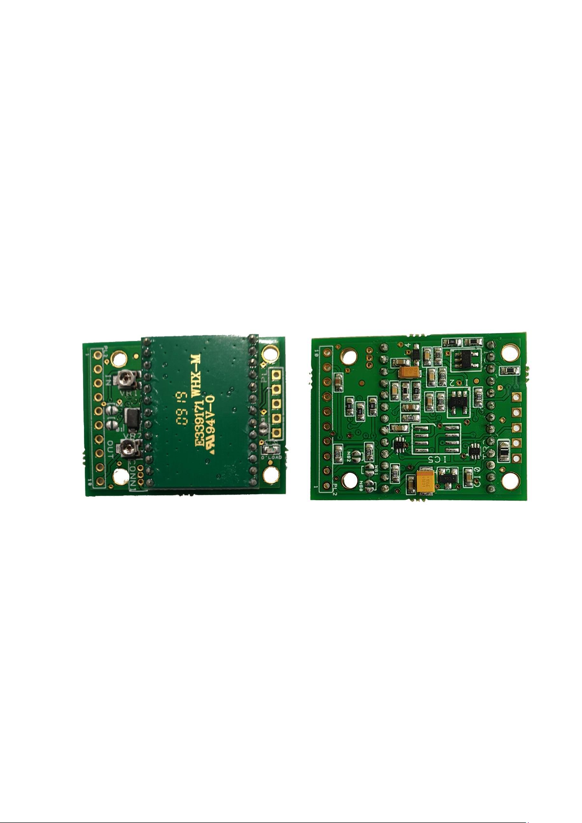
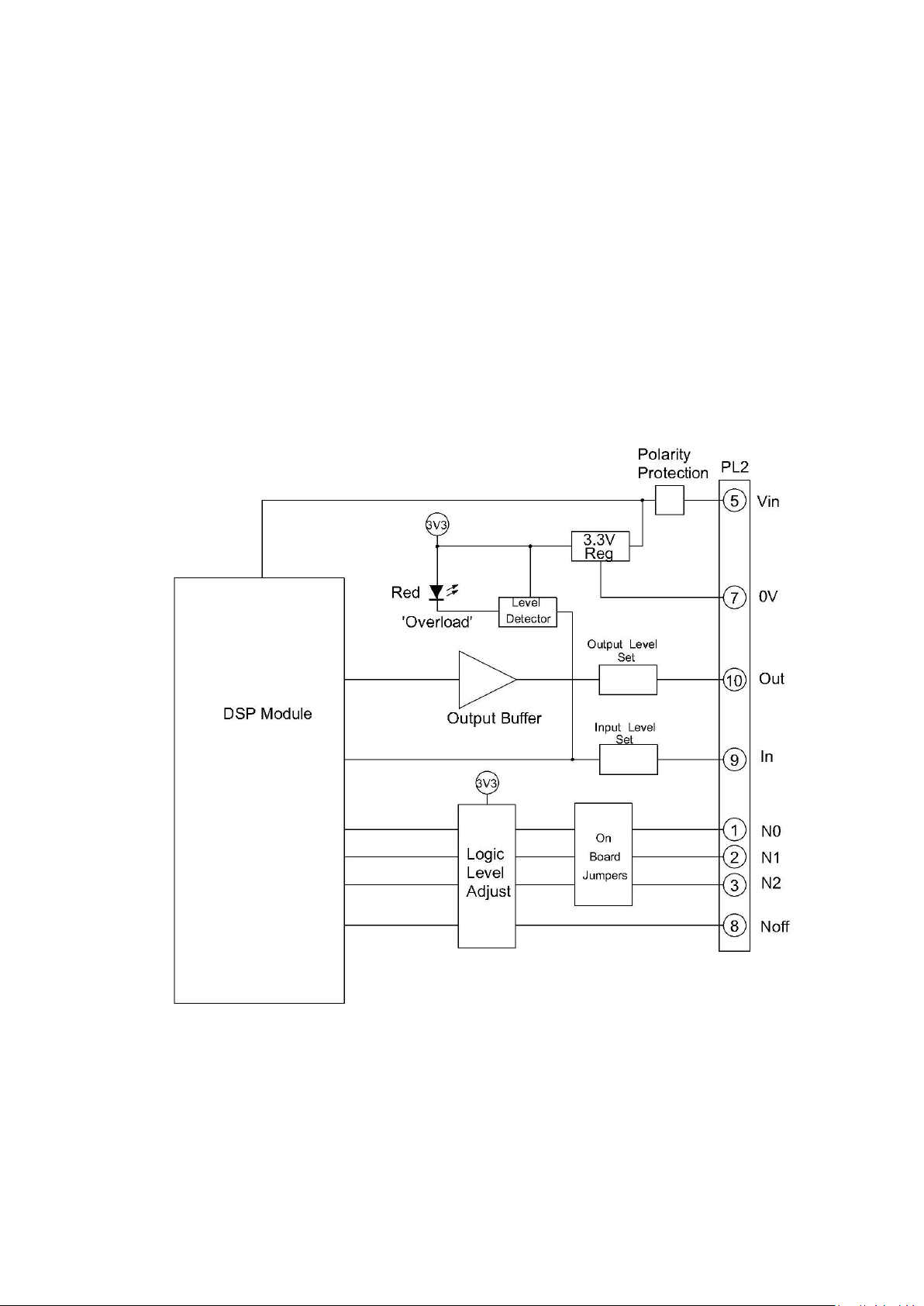
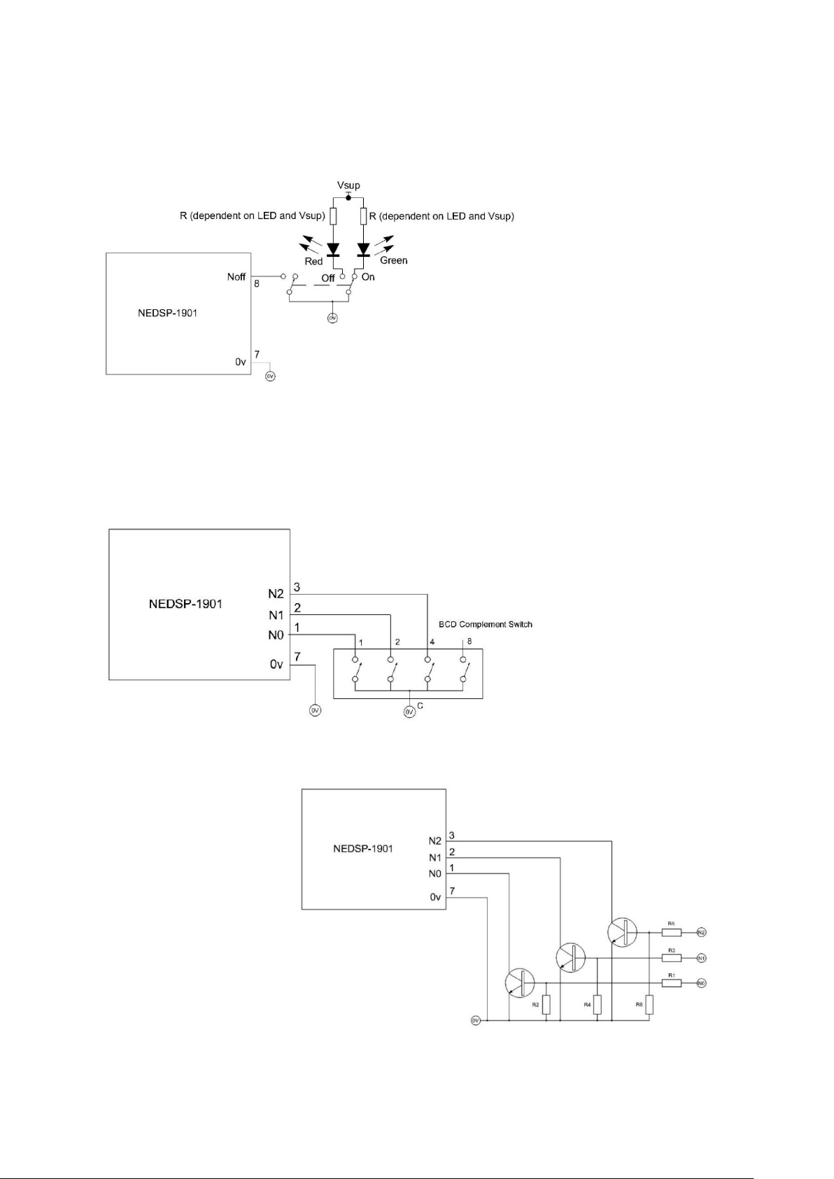
BHI NEDSP1901-PCB User manual

bhi
Copyright & Disclaimer:
Copyright: This publication, including all photographs and illustrations is protected under
international copyright laws, with all rights reserved. Neither this manual, nor any of the material
within, may be copied or reproduced without the written consent of bhi Ltd.
Disclaimer: The information in this document is subject to change without notice. bhi Ltd. makes no
representations or warranties with respect to the contents hereof and specifically disclaims any
implied warranties of merchantability or fitness for any particular purpose. Furthermore, bhi Ltd.
reserves the right to revise this publication and to make changes from time to time in the content
hereof without obligation of bhi Ltd. to notify any person of such revision or changes.
1. Introduction
The NEDSP1901-PCB module is an audio DSP noise cancelling module that is used to clean up noisy
speech signals to give improved speech clarity in noisy conditions. The 1901 module is pin for pin
replacement module for the discontinued NEDSP1061-PCB module. It operates with a similar
specification but incorporates the latest bhi DSP noise cancelling technology and maintains virtually
the same physical dimensions as the NEDSP1061-PCB.
DSP side of PCB Rear side of PCB
1.1 NEDSP 1901 Module Features:
•Fully adaptive to changing noise environments
•Input and output level controls
•Virtually no distortion to speech signals
•Up to 40 dB noise reduction in 8 selectable levels
•Audio bandwidth 300Hz to 5KHz
•Noise Reduction may be preset or remotely set during operation.
•7 to 18 Volt supply range
•Approximately 10 dB of signal gain with the ability to drive impedances of less than 1KOhm.
•Wide range of connection possibilities
•Mounting holes
1.2 Limitations
This module is designed to pass speech. Other signals such as data, music and morse (CW) will, to
some degree pass through, but the integrity of these signals cannot be guaranteed. Like the
NEDSP1061-PCB module it is designed to be placed in a low-level audio path (up to 1V p-p) only,
NEDSP1901-PCB User Manual Iss A
www.bhi-ltd.com

although there is a level adjustment on the module which will require adjustment. The output will
not drive a loudspeaker or other high-power load.
1.3 Module connection and Mounting
Connections to the module are made by a row of 10 plated through holes to one end which form
PL2. The holes are on a 2.54 mm (0.1”) pitch which allow the use of Straight or Right-angle pin
headers or direct wiring. This makes a flexible connection arrangement and allows the using to be
mounted either vertically or horizontally, plugged in or soldered directly to the target system.
PL1, seen on the right of the picture above,
is meant for programming of the 1901-KBD
module only.
Connections to the 1901 are via PL2, as
given in the table opposite.
Whichever method of connection is used,
ensure that the PCB is supported by using at least 2 of the M2.5 mounting holes to be found at the
corners of the board. It’s recommended that Nylon Securing hardware is used to ensure that
accidental shorts are avoided due to the fine nature of this PCB.
The Audio signal into the module is capacitor coupled to prevent DC offsets being affected.
Pin No
Name
Description
1
N0
BCD lsb noise reduction bit 0
2
N1
BCD noise reduction bit 1
3
N2
BCD msb noise reduction bit 2
4
N/C
Do Not Connect
5
Vin
Vin Supply Voltage (5V to 20 V)
6
N/C
Do Not Connect
7
0v
0V connection
8
Noff
Noise Reduction On/Off pin
9
In
Audio Input
10
Out
Audio Output
PL2 pin 1
Input Level adjustment
Output Level adjustment
PL2 pin
10
Overload
LED

An on-board voltage regulator allows the module to be used with a wide range of input voltages, but
to keep the power dissipation (and heat) down, it is advisable to use as low as possible supply
voltage. The power supply input is reverse polarity protected.
1.4 DSP Noise Reduction
The NEDSP1901 processes the incoming signal and uses known speech and noise patterns to
differentiate the speech from the noise. The unwanted noise and interference is then attenuated to
leave only speech.
The module has the facility
to be pre-set or adjusted
during operation. Digital
inputs control the functions.
These incorporate internal
pull-up resistors so they can
be left floating when not in
use.
The diagrams in Figure 1
(opposite) are taken from
actual audio signals and
illustrate how the signal is
being processed.
Figure 1 –Noise Cancellation

2.0 Module Description
2.1 Block Diagram
The NEDSP 1901 module has the facility to be preset or adjusted during operation. Digital input
control the functions. These incorporate internal pull-up resistors so they can be left floating when
not in use.
The audio signals into and out of the module are capacitor coupled to ensure that no DC levels are
pulled down or shorted when the module is used embodied as part of existing equipment.
The on-board voltage regulator allows the module to operate from a wide supply voltage (5 to 15
Volts) range. However, to keep the power dissipation (heat) down, it is advisable to use as low as
possible supply voltage. The Power supply input is reverse polarity protected.
Figure 2. NEDSP1901 Block Diagram

2.2 Module Layout
Figure 3 below shows the board dimension detail as seen from above. The overall thickness of the
board is 8.75mm. When considering the installation of this module, at least 9.5 mm height should be
provided, which will allow for the clearance of through-hole solder pins.
Figure 3. Board outline dimensions and mounting hole positions
The Jumpers NS0 through NS2 highlighted in Figure 4 are solder jumper pads to allow the user to fix
the Nosie Reduction level required. Care must be taken so as not to splash solder over un-used
solder pads when placing solder across the required jumpers.
Note: Ensure that any solder jumpers across these pads are removed before using the Remote Noise
Reduction control pins.
Figure 4. On-board Noise Reduction level selection jumpers
N0 solder
pad jumper
N1 solder
pad jumper
N2 solder
pad jumper

2.3 Pin Functions
The basic operation of the NEDSP pins are described below. More details may be found later in this
manual.
Pins 1-3 DSP Filter level set -These pins allow remote setting of the noise cancellation level. If these
pins are used, then ensure that the appropriate on-board pre-set solder jumpers are
removed (JP1 –JP3).
Pin 5 Supply Voltage - Supply voltage 5 V to 15 V DC
Pin 7 0V - This is the 0V pin and acts as a Star Point for all Audio and Power Grounds.
Pin 8 Noise Reduction On/Off - Connecting this pin to 0V inhibits the noise cancellation. Leave
this pin floating or tie it to +3.3 V to enable noise cancellation.
Pin 9 Audio Input - Audio Signal to be processed
Pin 10 Audio Output - DSP Processed signal from the module.
For optimum performance, keep all leads as short as possible. Use screened leads for the audio
signal and make sure that the 0V pin is grounded correctly with all signal grounds being reference to
this pin.
2.4 Controls
The audio level control potentiometers VR2 (Audio Out) and VR1 (Audio In) provide adjustment to
audio levels entering and leaving the module. Both controls are pre-set at the factory such that a 1V
p-p input provides a 1V p-p output with the Noise Reduction disabled.
To set the Input Level correctly, adjust VR1 until the ‘Overload’ indicator (LED1) just illuminates.
Then back off the potentiometer until the LED extinguishes. Turning the potentiometers clockwise
increases the levels.

2.5 Electrical Characteristics
Output impedance: 1k Ohms typical
Input impedance: 7.5k Ohms typical
Analogue Characteristics
Parameter
Description
Min.
Typ.
Max.
Units
Vin
Supply Voltage
5
8
15
V
Iin
Supply Current
15
20
mA
In
Audio Input Signal
10
500
mV (rms)
Out
Audio Output Signal
1000
Digital Characteristics
Parameter
Description
Min.
Typ.
Max.
Units
VHigh
High Level Input Voltage
-
3.3
5
V
VLow
Low level Input Voltage
0.8
-
-
V
3.0 Installation
The NEDSP1901 module is inserted into the path of the noisy audio. Adjusting the Input and Output
level controls allows the module to appear transparent to the audio signal level.
Figure5. General Audio signal flow with 1901 module installed
The NEDSP1901 requires a minimum signal level of 10mV rms or greater for optimum performance.
Signals lower than this may be used but the noise cancellation performance will be degraded as the
signal level drops. If the module is to be used with low level microphones, the signal will require
pre-amplification. The Output level control may be used to attenuate the signal back down to the
original signal level.

4.0 Functions
4.1 Noise Reduction Levels
8 Levels of noise reduction are available. Noise and tone reduction is shown in the table below:
Notes:
1. When processing signals with high levels of noise using the higher levels of Noise reduction,
the processed signal may sound a little strange. This quite normal with this type of signal.
2. Due to the adaptive nature of the noise cancellation algorithm, a small delay may be
experienced when the audio signal varies in the noise. For optimum performance the
module should be provided with a constant signal, for example if the module is installed into
a system employing a push to talk system, then the module should be inserted in the audio
path before any switching or muting. Thus, the signal will always be available for the
module to adapt to.
4.2 Setting different filter levels
The levels are set by applying a BCD code to three solder jumpers on the underside of the module.
The module can be controlled with a microcontroller. As the DSP employs internal pull-ups, it is not
necessary to drive the microcontroller pins high, they can be placed in a high impedance state.
4.3 Remote setting of DSP filter level
Remote setting of the DSP level may be achieved through the PCB connections at PL2, this allows the
filter level to be changed during operation. If the remote DSP settings are to be used, ensure that
the solder jumpers are removed from NS0 through NS2 as shown below:
To set the DSP level remotely, connect the pins N0, N1 and N2 (PL2 pins 1, 2 and 3 respectively) as
shown in Table 2 below.
Level
N2
N1
N0
1
0 V
0 V
0 V
2
0 V
0 V
+3.3 V
3
0 V
+3.3 V
0 V
4
0 V
+3.3 V
+3.3 V
5
+3.3 V
0 V
0 V
6
+3.3 V
0 V
+3.3 V
7
+3.3 V
+3.3 V
0 V
8
+3.3 V
+3.3 V
+3.3 V
Table 2 –Remote Pin settings for various Noise Reduction Levels
Level
Tone Reduction
White Noise
Reduction
1
4dB
8dB
2
5dB
12dB
3
6dB
16dB
4
8dB
20dB
5
16dB
25dB
6
21dB
30dB
7
25dB
35dB
8
65dB
40dB
The DSP Module has internal pull-ups on its inputs, so any cell in the table containing +3.3 V may be taken up to or left open
circuit.

4.4 Setting the Noise Reduction Level using the On-board Jumper links
The on-board Noise reduction selection jumper selectors are located on the underside of the
Module as shown below. These jumpers are actually PCB pads that should be linked using a solder
bridge. Caution should be used when carrying out this operation to ensure that other components
and connections are not bridged as this could cause the module to malfunction or even fail.
The Noise reduction Level settings
are shown in the table below.
Table 3 –On-board Jumper settings
4.5 Noise Reduction On/Off
The module has the provision for remotely enabling and disabling the noise reduction, while in
operation. The default setting for the module is noise reduction ON. This may be switched by the use
of the noise cancellation On/Off pin (PL2 pin 8). To inhibit noise reduction, connect this pin to 0V. To
enable the noise reduction, leave the pin unconnected.
The module may be controlled with a microprocessor. As the 1901 Module employs internal pull-
ups, it is not necessary to drive the microprocessor port pins high, they can be placed in a high
impedance state.
It should be noted that the 1901 module operates with 3.3 Volt logic signals. Therefore, if it is
intended that the Microprocessor is to drive the 1901 lines High, the Microprocessor should be
operating from a 3.3 Volt supply as well. Alternatively, the control signals may be attenuated using a
simple potential divider as discussed in section 5.
Level
NS2
NS1
NS0
1
Open
Open
Open
2
Open
Open
Linked
3
Open
Linked
Open
4
Open
Linked
Linked
5
Linked
Open
Open
6
Linked
Open
Linked
7
Linked
Linked
Open
8
Linked
Linked
Linked
NS0
NS1
NS2

5. Application Notes
5.1 Noise Cancellation On/Off with indication
In the example opposite a
Tricolour (or separate Red and
Green) LED’s are used to give a
visual indication of the Noise
Reduction mode. The Green
LED will illuminate when the
Noise Reduction is On and the
Red will illuminate when the
Noise Reduction is Off.
Figure 7. Noise Reduction On/Off with Red/Green LED Status indicator
5.2 Remote adjustment of Noise Reduction level
This section illustrates the various options for altering the DSP level remotely, during operation.
Figure 8. Basic setting using a BCD switch with complementary logic .
The transistors allow
interfacing with higher
voltages to control the DSP
level. As a rough guide the
Resistors R1, R3, R5 can be
around
10 kOhm. Resistors R2, R4
and R6 could be in the
range 2.2 kOhm for control
voltages over 10 Volts and
4.7 kOhm for voltages
between 5 Volts and 10
Volts.
Figure 9. Noise Reduction setting using a Transistors

The module can be controlled with a
microcontroller. It is not necessary to
drive the control pins with the controller
as the NEDSP has internal pull-up
resistors. Therefore, the microcontroller
would operate pulling Low or in a High
impedance state.
Figure 10 –Operation with a Microcontroller
Important Note: If the Microcontroller is driving the control pins both High and Low, it should be
operate from a 3.3 Volt supply only. If this can’t be achieved, then consider using either the
Transistor method of interfacing above or the much simpler voltage divider method outlines for 5
Volt operation shown in Figure 11.
If a Microcontroller
operating on 5 Volts is to
be used to drive the
NEDSP1901 control pins,
make sure that the drive
voltage is no higher than
3.3 Volts. Alternatively, if
the Microcontroller is
operating on 5 Volts,
insert a simple Voltage
divider circuit between
the control pins and the
microcontroller.
Figure 11. Alternative method of controlling the NEDSP1901 with 5 Volt logic.
For +5 Volts, the suggested values for R1, R3 and R5 is 1 kOhm, while R2, R4 and R6 should be 1.5
kOhm.
5.3 Audio Bypass
In safety critical applications, a bypass system should be included to maintain communications in the
unlikely event of the
NEDSP1901 or power
failing. The following circuit
uses a relay to route the
audio signal directly. In the
event that the power fails,
the Relay will de-energise
and connect the Input to
the Output directly. It will
be noted that a switch has
been included to allow the
signal to bypass the
Module.
Figure 12. Typical Relay operated audio bypass circuit with user Power Off/Bypass switch

Contact details:
bhi Ltd
PO Box 318
Burgess Hill
West Sussex
RH15 9NR
Tel: +44 (0)1444 870333
Email: sales@bhi-ltd.com
Web: www.bhi-ltd.com
Other manuals for NEDSP1901-PCB
1
Other BHI Control Unit manuals
Popular Control Unit manuals by other brands

LK Systems
LK Systems ICS.2 Assembly instructions

Wintal
Wintal 3-Way HDMI Selector instruction manual

WABCO
WABCO MICO ACV-SMO Product Explanation, Operating Information, and Service Instructions

Singer
Singer 106-A-Type 3 Installation, Operating and Maintenance Instruction

Comelit
Comelit FT/GEN/05 Technical manual

Seav
Seav BeWeather manual

Purified Air
Purified Air UV-O 500 Technical and Operations Manual

Freescale Semiconductor
Freescale Semiconductor TWR-LCD quick start guide

Val Controls
Val Controls I 24-AF Series Replacement guide

Leonard
Leonard ECO-MIX 269-LF INSTALLATION ADJUSTMENT SERVICE

Lawler
Lawler NEPTUNE EMX 075 Installation & maintenance manual

WABCO
WABCO 461 307 Test instruction