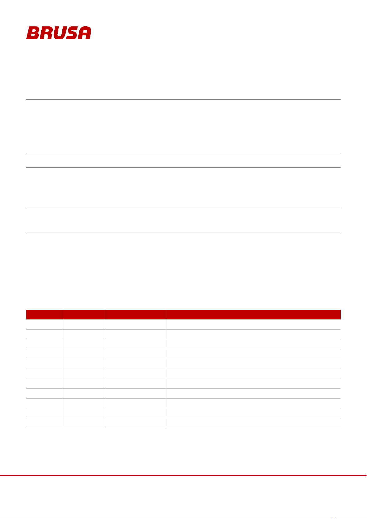
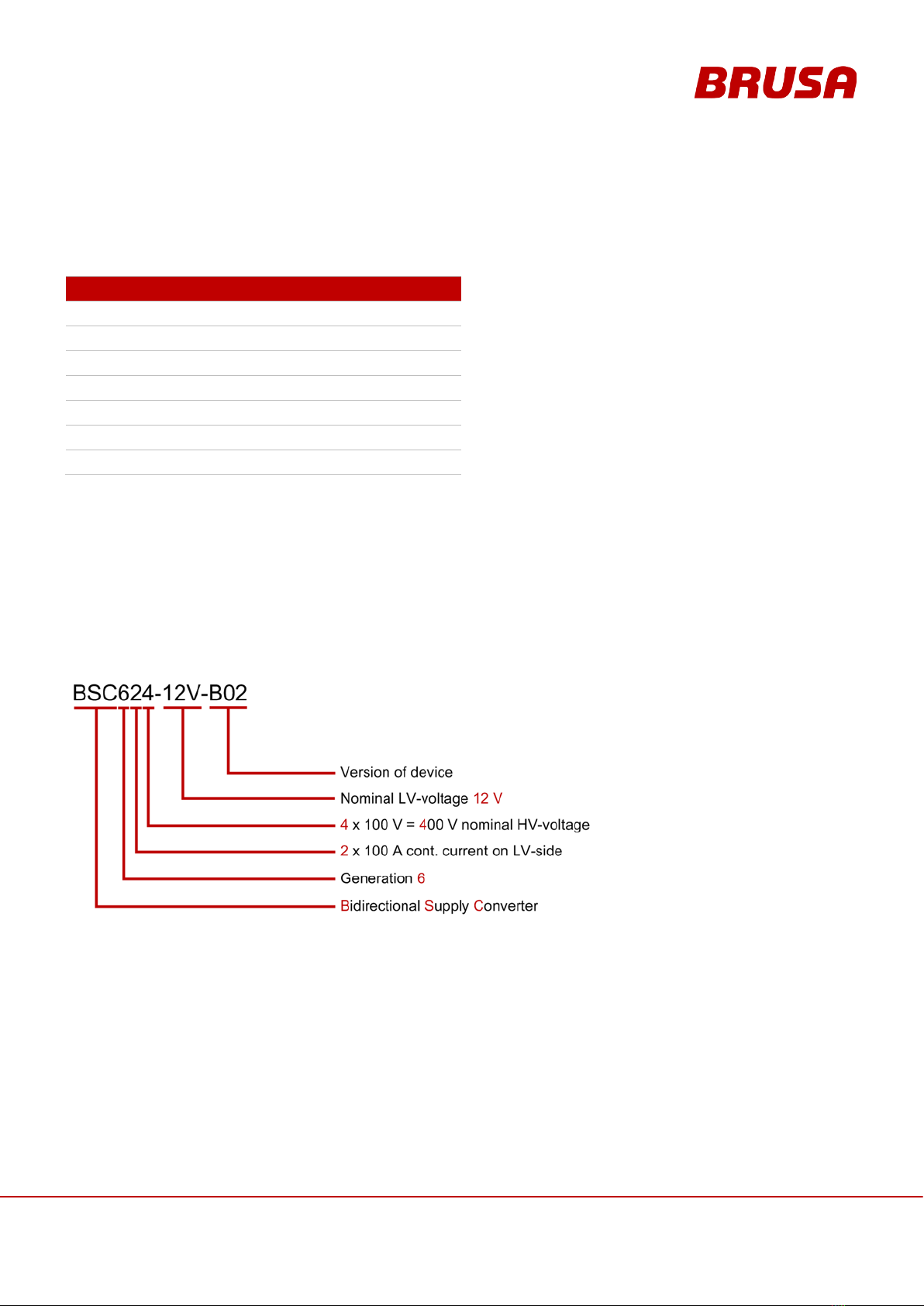
Technical information
and start-up
6.2 Technical properties.................................................................................................................25
6.3 Block diagram BSC624-12V-B .................................................................................................25
6.4 Basic function / EMC concept...................................................................................................26
6.4.1 Topology benefits..............................................................................................................26
6.4.2 Internal current supplies....................................................................................................27
6.4.3 LV filter concept ................................................................................................................28
6.4.4 HV filter concept................................................................................................................29
6.4.5 AUX filter concept .............................................................................................................30
6.5 Warnings on the device............................................................................................................31
6.6 Vehicle installation basic principle............................................................................................32
6.7 Safety concept vehicle installation............................................................................................33
6.7.1 Principle of operation Interlock ..........................................................................................33
6.8 Overview of the main structural components............................................................................34
6.9 Dimensions and installation information ...................................................................................35
6.9.1 Fixing points......................................................................................................................35
6.9.2 Dimensions .......................................................................................................................36
6.9.3 Installation position............................................................................................................36
7Electrical interfaces...........................................................................................................38
7.1 Pin assignment of control connector (device side)....................................................................39
7.1.1 Pin 1 GND.........................................................................................................................40
7.1.2 Pin 2 AUX .........................................................................................................................41
7.1.3 Pin 3 EN............................................................................................................................42
7.1.4 Pin 4 DO0 – pin 7 DO3......................................................................................................43
7.1.5 Pin 8 PG1, pin 14 PG2, pin 15 PG3 ..................................................................................44
7.1.6 Pin 9 CNL, pin 10 CNH .....................................................................................................44
7.1.7 Pin 11 TXD, pin 12 RXD....................................................................................................45
7.1.8 Pin 13 PRO.......................................................................................................................46
7.1.9 Pin 16 DI0, pin 17 DI1, pin 18 DI2.....................................................................................46
7.1.10 Pin 19 IL1, pin 20 IL2 ........................................................................................................47
7.1.11 Pin 21 AI1, pin 22 AI2, pin 23 AI3......................................................................................49
7.2 Pin assignment of HV power connector (device side)...............................................................50
7.3 Pin assignment of LV power connector (device side) ...............................................................50
8Connections.......................................................................................................................51