BugBrand WOM User manual

BugBrand Workshop Oscillator Machine
Version3.1 October 2010
Welcome!
We're going to put together a little circuit board noise machine and, along the way, get an
introduction to some electronics and soldering techniques.
Don't worry if you've never done any electronics before – many people with zero prior
knowledge have successfully built this machine in only a few hours. Also, while this handout
contains quite a lot of information, much of it may go over your head for now – electronics
can be seriously confusing to begin with (I certainly found this!), but hopefully you can come
back to this information at a later date and gradually the pieces should begin to make sense.
It is also fine, of course, just to build the machine and enjoy it!
All the parts are included in the kit – all you need is a soldering iron, some solder and a pair
of wire cutters (more details in Sections 1).
The machine we'll make contains:
●
Three oscillators – the sound sources
●
A mixer – to blend the oscillators together
●
Simple tone control – to shape the sound
●
Jack output and mini-amp
●
Circuit bends – 11 body contacts + power starvation
Parts of this document:
1. The parts of the kit & tools required
2. Soldering & building
3. Examination of the circuit workings
4. Further reading & final notes
Plus in the separate document:
Full Schematic // Parts Placement // Large image of Completed Board // Bill of Materials
(Note – Version 3.0 was done Nov2009 and most of the photos were taken then so some
pictures are very slightly different from the kits today!)
If you have questions while building, probably the best place to ask is on the Muff Wiggler
Forum Thread: http://www.muffwiggler.com/forum/viewtopic.php?p=25190
Or you can contact me directly: tom@bugbrand.co.uk
Good Luck!
& thanks!
Tom Bugs
www.bugbrand.co.uk
The documents (in colour) can be downloaded from here:
http://www.bugbrand.co.uk/docs/bugbrand_WOM_main.pdf
http://www.bugbrand.co.uk/docs/bugbrand_WOM_schem_bom.pdf
1 – Parts of the kit & tools required
Carefully open up the main bag of parts – be careful as there are some small bits within! I'd
recommend that you don't open up the smaller inner bags for now – wait until the building
stage. Let's examine what we've got:
Contents (from top left): Resistors, Capacitors, ICs + Holders, PCB, Dials, Switches +
Speaker, Battery + Holder
You may want to have the circuit schematic sheet on hand now so you can begin to compare
the parts discussed with what is drawn in the schematic – we'll introduce some symbols and
terminology. By the way, a schematic is just a diagrammatic representation of the electronic
circuit – it shows which parts connect together, though it doesn't show the actual layout of
the printed circuit board (PCB) – more on that later. Let's also note that much of this
introduction is quite specific to this kit but should still be relevant to electronics in general.
We'll begin with the Battery (which comes with a holder and bolt to attach the
holder). This will be the power for the circuit – the battery is a 9volt supply and we'll
use the terminology of V+ for the positive connection and Ground (Gnd) for the
negative connection. On the main schematic all points with the Gnd symbol are
physically connected together in the circuit (and the same for the V+ points).
Now take the Resistor bag (which also contains a couple of
diodes). Resistors oppose the flow of electrical current and
come in many different values measured in Ohms (Ω) or, more
usually, thousands of Ohms – kilohms (kΩ) – or even millions
of Ohms – megohms (MΩ). By the way, we usually write 4700
ohms as 4k7 (we know that they're in ohms so there's no need
to write the Ωsymbol). If you look closely you will see various
coloured bands around each resistor – these identify the
particular value, and we'll examine these in the next section
(note – to avoid confusion, keep the resistors on the paper
strips until you're about to use them!). Resistors are non-
polarized components– it doesn't matter which way around they go.
In the bag there are also two types of Diode – these allow current to flow in one direction
only. Note the black ring around one end as this shows which way around to use them. The
smaller diodes are 1N4148 silicon diodes which are commonly used, while the large one is a
1N4001 rectifier diode which we'll use to provide battery polarity protection.

On to the Capacitors – there are three types of
various values in the bag. Capacitors (or caps)
store electrical energy and are measured in
fractions of Farads – our typical values are in
picofarads (pF), nanofarads (nF) and microfarads
(
µ
f or uf) - 1000pF equals 1nF and 1000nF equals
1uf. We have two types of low value caps here –
the blue dipped-ceramic and the yellow polyester-
box type (these types are pretty similar for our
purposes) – note that these types are both non-
polarized. There are also the black cylindrical electrolytic caps. These ones are polarized
and must be used the correct way around – they have a positive side (the straight line on the
schematic symbol and the long leg on the actual cap) and a negative side (the short leg on
the cap – also there is a white stripe on this side with a minus symbol). We'll discuss more
about the use of these capacitors when we look at the circuitry in the next section.
The next parts to consider are the chips or Integrated Circuits (ICs). These come in a little
piece of foam along with IC holders for them – ICs can be sensitive (to heat or static
electricity) so we generally attach a holder to the PCB first and only add the ICs once the
circuit is complete (this also allows easy replacement if something breaks). There are literally
thousands of different types of ICs available today and within the fairly nondescript black
packages they actually contain miniature
electronic circuits (composed of parts like
resistors, capacitors, transistors etc). ICs have a
number of pins (or legs) – typically 8 or 14 in our
types of circuit – and these must be connected the
right way around for correct operation (indeed, a
chip will likely be killed if connected the wrong way
around!). Examining an IC you will notice a notch
at one end (or sometimes just a dot) – the pin to
the left of this is Pin1 and the numbering from here
goes down that side and then up the other. It is
beyond our scope to look into the vast variety of
chip functions available, but let's look at one type
that we're using and see how the package and
schematics hook up.
The two 14pin ICs we have are actually quite
similar to one another – they are both members of
the 4000 series CMOS Digital Family. One of the
best ways to find out information about an IC is to
go to Google and search for the datasheet. We'll
look at the 4069 so you could search for '4069
Datasheet'. We see that this chip is called a Hex Inverter – hex means it contains six
sections (gates) and the sections function as Inverters. Looking at the Pin Connection
diagram you can see how the six sections connect to the pins of the chip. Two pins are left
over and these are the power pins – pin7 is labeled Vss and this connects to Gnd, while
pin14 is called Vdd and will connect to V+. The scheme of having the Gnd pin at bottom right
and V+ pin at top left is actually universal throughout the 4000series CMOS family. Also note
that the Pin Connection for the 40106 happens to be very similar to the 4069 – it is a Hex
Schmitt Inverter and also has 6 sections connected in the same way, but the sections
provide slightly different functions from the 4069.
The next bag contains the dials or Potentiometers
(Pots). These are parts we use to control the
behaviour of the circuit. While the ones we're using
are small, they're pretty much the same as big dials
on HiFi systems or synths. Pots are variable
resistive elements with three pins and we'll use
them in one of two ways. The first way (shown on
the right) is called a Potential Divider (you can
check Wikipedia for a more detailed explanation).
There is a fixed value resistance between the outer
pins (1 and 3) and then a wiper that moves
between them as you move the dial. The way shown is used to attenuate a signal – ie as a
volume control – turned one way the full signal is passed while turning the other way will
make no signal pass. The second application involves tying two of the pins together to give
a variable resistor, a useful means of controlling the behaviour of a circuit – more details on
this in the circuitry section.
The last bag contains the final parts including the
switches which allow us to select different behaviours.
Mechanical switches are common in day to day life so
should require little introduction. These particular ones
have three terminals (the other legs are just for adding
stability) – when the switch is pushed one way then pins
1 & 2 are connected together, while the other way
connects pins 2 & 3, thus allowing us to select different routes within the circuitry.
There's not much left to examine – the Speaker should be
self-explanatory but lets just look at the Jack Socket. This is
a switched mono 1/4” socket (ie for standard guitar cable). It
has four legs, two on each side. The signal goes out on to
the tip of the jack plug and the sleeve connects to the circuit
Gnd. Note also that when no jack plug is inserted the legs on
either side are connected – this allows us to automatically
switch off the mini-speaker when a cable is plugged in.
When the plug is inserted the horizontal pieces of metal are
lifted up and thus the legs on the lower side are left unconnected.
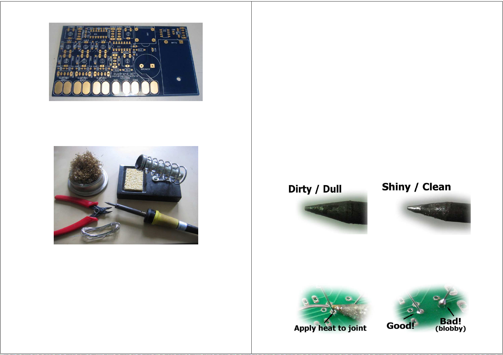
Finally lets take a quick look at the Printed Circuit Board (PCB). This has been specifically
designed for this project – laid out directly from the schematic diagram and fabricated in a
far-away land! Its actually quite a complex procedure to do such a design and for most one-
off circuits you'd simply use a material called stripboard (look it up) but for replicatable
projects it really makes sense – everything is laid out nicely and building errors are
minimized. If you examine the PCB you'll see tracks on the top and bottom of the board
joining the different parts together. The gold coloured pads for the components make
soldering easy (hopefully!). Now, people have asked why we make this project directly on the
PCB without using a box. I've found that these on-board-circuits are strong and reliable. The
time saved by avoiding putting it in a box is quite considerable and it also makes the project
a good deal less complicated. Over the years I've been building things I've found that the
most time consuming part of making devices is the boxing – wiring up pots and other
controls. The wiring is also a place were faults can easily develop and my aim for this project
has really been to make something that is almost guaranteed to work first time – the one
thing that kills a buzz for electronics really quickly is when you finish building something and
then it doesn't work!

Tools
There's another factor in my choice of mounting everything on the PCB – hardly any tools
are required for the building! All that is required is a soldering iron (plus stand), something for
cleaning the soldering iron (either a dampened sponge or brass wool tip cleaner), some
solder (naturally!) and a pair of wire cutters (ideally a small pair though larger ones will do
the job). There are more notes on soldering and where to get an iron at the end of this
document in the appendix – have a check!
It is worth just mentioning how to set up a place to work – clear a good area so that things
won't get lost (as mentioned before, keep things in their bags until you're going to use them)
and find yourself a good source of light as you will find it extremely hard to solder without
enough light to see what you're doing! It's also worth locating yourself somewhere with good
ventilation, perhaps next to an open window – while the fumes from soldering aren't
hazardous some people find them irritating.
2 – Soldering & Building
In the interest of keeping things interesting (!) we're going to move straight on to building
before examining the workings of the circuit – but we'll come back to that in the next section.
First let's talk about soldering. This is an area that often puts people off electronics, but with
a little info its actually very straight forward! Bad soldering is probably the largest factor in
crushing the enjoyment of electronics! Poor techniques will result in bad joints which don't
work or are intermittent – so pay close attention to the soldering and your project should
work first time.
It should go without saying that the iron is HOT and should be handled with care both to
avoid burning yourself and items / people around you!
Soldering is a process where a metal alloy (solder) is melted to join metal surfaces together.
For this we need heat – provided by the soldering iron. When you're starting out there really
is no need to shell out on an expensive iron – all the irons I use in my teaching workshops
cost under £5 (off eBay) and work just fine. What IS important is to keep the tip of the iron
clean – a dirty tip, even on a decent iron, won't allow good soldering!
Cleaning – a clean tip should appear shiny. If the tip is dull / dark grey then it needs to be
cleaned before soldering. The tip of a hot iron will gradually oxidize forming a thin layer of
oxide over the tip which isn't good for heat transfer. We use a cleaning sponge or brass-wool
cleaner to remove this layer and then melt a little solder onto the iron tip (a process known
as tinning). After this the tip should appear nice and shiny – if not, repeat the cleaning
process another time. The iron's tip should always be tinned when sitting in its holder – I
always clean and re-tin the tip when I put down the iron after soldering and then clean it
again when I pick it up.
Soldering – the aim of soldering is to heat up both the component lead and the PCB pad.
Once they're heated enough, solder is melted onto the join and it flows around the
component lead to form a solid seal. We must do this relatively quickly to prevent damage to
the component or board (certainly no longer than 5seconds but preferably around 1second).
We need to apply enough solder to fully cover the seal, but not too much as to make a
bulbous joint (as this can hide problems). The join should appear clean and shiny – not a dull
grey – and should be slightly concave.

So, follow this order each time:
●
Clean the tip
●
Tin the tip
●
Heat the joint of lead and pad
●
Flow the solder
●
[Solder further joints if required, cleaning the tip as necessary (c. every 5 – 10 joints)]
●
Clean and re-tin the tip before replacing the iron in its holder
You may also want to think about how you hold the iron and how you position your hands for
the work. I hold the iron in my right-hand (as I am right-handed!) and then the lower side of
my hand rests on the desk – this gives a very stable position for working. I then turn the PCB
in whatever direction is needed to get good access to the point of soldering. The left-hand is
multi-tasking – I use it to feed solder into the join and sometimes use my fingers to hold the
PCB steady at the same time.
If you do notice a bad joint then it is always possible to reflow the solder and fix the problem
– either just reheat the joint until it flows properly or desolder it and reapply fresh solder.
Just a couple of notes on solder - firstly, while solder used to generally contain Lead (a
poisonous metal) most of Europe now uses Lead-Free solder due to the RoHS (Restriction
of Hazardous Substances) Directive. My PCBs are all made to Lead-free standards and all
components I supply are also Lead-free. Also note that solder wire generally contains a core
of a substance called flux – a chemical cleaning agent that facilitates soldering. This can
sometimes splutter a little when soldering and may leave a little residue around the solder
joint (which isn't generally a problem – but it can be cleaned off if required). Flux is also
responsible for the smoke that occurs when soldering – this smoke is generally harmless but
may cause some respiratory irritation, especially for asthmatics, so if possible work
somewhere with good ventilation (by a fan or window).
Desoldering – if you make a mistake you may have to remove some solder and this is
actually a little tricky with these fabricated PCBs – so try to avoid mistakes in the first place!
There are two methods possible – a solder-sucker or desoldering braid.
A solder-sucker is vacuum pump which sucks up molten solder. You depress the plunger,
use the iron to melt the solder to be removed, place the tip of the sucker by the melted joint
and then press the button to suck. Unfortunately, this technique tends not to work so well on
fabricated PCBs due to the though-hole plating.
Desoldering braid draws up molten solder by
capillary action. You put the braid on top of the solder
to be removed and press the iron tip on top, melting
the solder into the braid. It is generally necessary to
pull the braid across the join to remove all the solder
– a technique that takes a little practice!
Ok – finally the time comes to build...
(you may want to turn on your soldering iron at this point to let it heat up)
But first:
●
Don't rush! Double check everything before soldering – ask if you have problems!
Better to move slowly than to make errors.
●
Keep that iron clean!
Proceeding in a methodical manner is of vital importance – do things by stages so that you
don't confuse yourself and to avoid components getting mixed up (keep things in their bags
until you'll use them). We generally build from lowest profile (height) component upwards –
so we start with resistors and move from there. It may be a good idea to work along with the
Bill of Materials sheet (BOM) as this lists the components in the order you'll put them in. You
may like to cross the items off as you solder them in place.
We'll start with the two small silicon diodes – examine them and observe the black band
around one end. Now locate the positions for D1 and D2 on the PCB and note that there's a
line marked on them – this shows the correct orientation of the diodes (these are polarized
components and must go the correct way around). You will also notice that one pad is round,
the other is square – the band on the diode should go to the square hole. Remove one of the
diodes from the paper strip and bend the leads at right-angles as shown – the bends should
be tight to the body so the diode will fit snuggly into the PCB and fit right up to the board.
Turn the board over making sure the diode stays in position – you can splay the legs out
slightly to prevent the component moving about. Now have a go at soldering, remembering
the order: clean tip -> tin tip -> heat join -> flow solder -> clean, tin and replace. If all goes
correctly you should have two nice clean solder joints. If you've done that ok then you can
snip the leads off just above the join – nice and neat.
Do the same for the other diode – hopefully you'll be getting a feel for how the solder and
iron work and feel... From there we move to the resistors – you may prefer at this point to
start placing several components at a time before soldering them all. Though – don't put
them all in at once or you'll find all the legs get in the way!

While most circuits will make use of a wide variety
of resistor values, this kit is designed with simplicity
in mind so we've only got three different values. As
mentioned, the coloured bands on the resistor's
body show the resistance value – do a Google
search for more information. The resistors we use
have the following colours:
•
1K: Brown/Black/Black/Brown/Brown
•
10k: Brown/Black/Black/Red/Brown
•
1M: Brown/Black/Black/Yellow/Brown
As you can see, all the colours are the same
except for the fourth band as the resistors are all
multiples of 100 ohms. (remember that 1M means
1000K). You may prefer just to keep the resistors attached to the paper strips and figure out
the values by deduction – there's just one 1M, two 1Ks and ten 10Ks.
Let's begin with the 1Ks (R10 & R12) and the single 1M (R9) located as shown below. Do the
usual steps of bending the legs close to the body, put them in place and solder. Note that
resistors are not polarized – it doesn't matter which way around they go. I find when I'm
soldering that I turn the board round to find the best way to get the iron tip to the solder joint.
Also be careful not to inadvertently solder up any extra holes with a careless movement of
the iron!
To finish up the resistors we fill up all the remaining spaces with the ten 10Ks – R1, R2, R3,
R4, R5, R6, R7, R8, R11, R13:
We finish off these first steps by adding the power diode (D90) to the top left corner of the
board, by the battery box and the On/Off switch.
Hopefully all your resistors and diodes are now in place and properly soldered!
Next come the holders for the ICs which are held in the piece of foam (note: NOT the actual
ICs!). You should have one 8pin socket and two 14pin ones. Note the notch at one end of
each holder and, identifying the placements IC1-3, line up the holders with the PCB
markings. Now – you'll probably notice that when you turn the PCB upside down to continue
soldering that all the IC holders fall out! I suggest holding the holder in place with a finger,
turning the board upside down and then bending out a pin on each side to hold the holder in
place before soldering (do this one by one for each IC holder).
Before soldering make absolutely sure that all the legs have correctly gone through their
holes (sometimes legs get bent under the holder) – if you start soldering before noticing such
a problem then you've got a right task trying to desolder things and sort out the problem! And
make sure you solder all the pins – don't inadvertently miss any!

Capacitors come next – find the bag and empty them out. There are three types – there's a
single blue dipped ceramic, various yellow or blue poly-boxes and the black tower
electrolytics. We'll put each group in separately, so start with the blue ceramic (C4). You may
notice that numbers are printed on the side (maybe hard to read!) - it should say 103 which
means 10 plus Three Zeroes – ie: 10,000pF or 10nF.
Note that the ceramic and polybox caps are not polarized – they can go in either way
around, so locate the positions, put the caps in, solder and trim....
On to the poly box caps. These have a slightly confusing number system (this actually varies
a lot between different types and makes of capacitor) so make sure to sort them out correctly
using the pictures below as a guide. There are two blue boxes – the small one is the 10n cap
(for the Tone control) while the big one is the 680n (marked on the cap as u68). The single
22n, 47n and 470n are quite clearly marked on top, but the 100n and 220n (4 of these) are
confusing as these are written .1 and .2. By the way, the extra letters/numbers indicate the
maximum voltage rating for these caps (63v or 100v).
It is important that you identify the caps correctly as otherwise the WOM may work
strangely – double check with the picture below before soldering!
Now, the final electrolytic caps are polarized and so must be put in the correct way around
(they can pop if connected back-to-front!). If you examine them you will see that:
●
the value and voltage rating are marked in small letters on the side (eg 100u 10v –
you can ignore the voltage marking)
●
next to this is a vertical white(ish) strip with minus signs marked – this shows the
negative lead which will go to the round pad
●
the legs are also of different lengths – the short one corresponds to negative and the
longer one is positive (goes to the square hole)
If it is hard to read the numbers off the side you can probably identify the different caps by
process of elimination! There are two small 4u7 caps (C9 and C91), one slightly larger 100u
cap (C10) and then one much larger 470u cap (C90) – we'll keep C90 off for now due to its
larger size. Remember – the long lead goes to the square hole!
Time for the controls – the pots. You can leave off the spindle dials until the end, so put them
back in the bag and sort out the different value pots. There should be two marked as 10k
(Tone and Level) and then seven remaining all with 1M (OSC1-3, LVL1-3, Starve).
You'll probably find that, like the IC holders, the pots often don't want to stay in place before
soldering, so here's a technique. Begin with just one pot for example one of the 10Ks to go in
the Tone position. Firstly, hold the pot roughly in position with a finger and turn the board
upside down. We want to just tack a little solder onto one of the legs to hold the pot in place
– it doesn't matter if the pot is slightly out of position for now. With the pot held roughly, pick
up the board, still keeping it upside down, and put a finger of your left hand onto the pot from
underneath. While pressing on the pot, reflow the single solder connection until it melts – at
this point the pot (which you're pressing) will pop into the correct position! Once that's done,
you can solder the remaining legs. Use the same technique for the other 10K pot and then fill
the other spaces with the 1M ones.

This method of soldering one leg, then pressing and reflowing the solder is used again for
the final few components. We'll first do the eight switches (which can go in either way
around), followed by the mini-speaker (+ goes to the square hole), the remaining electrolytic
capacitor (C90 – the large one), the jack socket and, finally, the battery box (which definitely
does need to be pressed down during soldering). Once all those are attached successfully
you are almost done (and maybe switch the iron off now!). Turn the board over again and,
after trimming any stray legs, thoroughly eyeball all the joints to check that they are all good
– just reflow or resolder any that don't look right. You can also add the spindles to the pots
and the little nylon bolt and metal nut to hold the battery case firmly on the board. (leave the
rubber feet off for now though and don't put in the battery yet)
Your board should now look like this from on top and nice and tidy underneath!
Now that all the soldering is done we can finally put the chips in. This is actually a little fiddly
– ICs come with their legs slightly splayed meaning they don't always slot straight into the
holders. You should also note that the two larger ICs are static sensitive – you need to
discharge any static charge from your body before taking the chips from the foam. To
ground yourself, simply touch something metal that is connected to the building's earth line.
For example: a radiator (an unpainted part), the metal case of a
computer or something similar.
Lets quickly identify the chips. Reading the codes off the top of
the chips you'll notice there are lots of other letters and numbers
– just ignore them! (they are date codes etc) The two larger 14pin
chips should be identified as a 40106 (IC1) and a 4069 (IC2) and
the 8pin chip can be seen to be an LM386 (IC3). Notice also the
notch or dot at one end of the chip – this identifies the correct
orientation and should match the notch of the corresponding IC
holder. Make absolutely sure you place chips the right way round
– powering up a chip the wrong way round will generally kill it
instantly. See the next page for a picture. Ok, the methods:
Technique 1 – pick up the chip and orientate it.
Gently position the legs of one side into one
side of the IC holder. Holding the chip at an
angle of about 35deg, apply a gentle pressure in
the direction shown so that the legs bend very
slightly – don't push too hard or the legs will all
bend out of shape! Gradually bring the other
side of the IC down to locate the rest of the legs
into their sockets – once things are in position,
apply a final downward pressure to fully seat the
chip.
Technique 2 – pick up the chip, holding it lightly
at each end. Turn the chip on its side so it sits
on one set of legs then apply gentle downward
pressure to slightly bend the legs. Be careful to
apply pressure evenly at each end and also to
avoid bending the upper pins with you fingers.
The legs need only be bent less than a
millimeter so be gentle! Turn the chip over and
do the same to the other side. The legs should
now be ready to slot easily into the holder –
orientate the chip lightly in the socket, double
check all the legs are seated correctly and only
then apply downward pressure.
Ok – time for the moment of truth! Unwrap the battery and clip it into place (make sure the
polarity is right before switching on!). I'd say give one final check over before switching on,
but you've probably already launched straight on in and are hopefully already making a
hearty racket!
You can finish things off by attaching the rubber feet to the underside.

What happens, though, if it doesn't work? That's a tricky one and frustrating too... There are
several areas to start checking:
●
double check the orientation of the ICs and that the chips are in the correct positions.
●
bad soldering – this is probably the most common mistake when starting out. Check
and check again that all the joints are good – it can often take a while to spot (maybe
take a break and come back a bit later). Pay attention to joints that look overly
bulbous, as underneath the solder it may be that the component isn't actually poking
through at all... If things look suspect then it may be good to desolder and then
resolder to be sure.
●
check also that all the leads are properly snipped close – I've seen short leads left
which then bend over to cause a short circuit.
●
In a similar manner, check that adjacent pads haven't been accidentally soldered
together (something called a solder bridge) – again, desolder and repair when things
look suspect.
●
Check all the solder joints once again!
Section 3 – Workings & Circuitry
I always reckon that the best way to learn an instrument like this is to just dive in and
discover! Controls are labeled (..a bit small perhaps..) so that may give some clues too. But,
there'll come a time when you may want to know more. So lets look at the controls and then
at the circuitry that's making it all tick.
As described at the start, the circuit we've got contains:
3 Oscillators -> Mixer -> Tone Control -> Output -> Mini-Amp
The circuit board has been laid out in a way that is (hopefully!) quite logical – imagine the
signal flowing from left to right, beginning with the oscillators, mixing these and shaping the
tones before outputting the sounds.
Oscillators:
–
Each has a Range switch (Lo rate = left, Hi rate = right), a Pitch dial and a Level
control that sets the volume to the mixer.
–
The Starve control effects all three Oscs by simulating the battery running out of
power. Turning the dial fully clockwise means full power. This is coupled with the
Stable switch which changes the behaviour when the power is starved.
–
The Sync switches are used to 'synchronize' Oscs 2 & 3 to the rate of Osc1 to give a
rich harmonic sound (look on the Internet for more details on Sync!). Note that for an
Osc to be sync'd it must be running at a higher pitch than Osc1 otherwise no sound
will be heard. It also works best when the Oscs are run at full power.
Mixer & Tone:
–
The three Osc signals are mixed via their Level controls. The mixer has a Boost
switch which changes its gain – this is especially useful when the Osc section is
power starved as the amplitude of the waveforms drops dramatically and this Boost
helps maintain a relatively stable output volume.
–
The Tone control is a simple low-pass filter that cuts out treble frequencies. You may
not hear much with the onboard Mini-Amp but it is more noticeable when you plug into
an external sound system.
–
You will find that the sound and behaviour change quite a lot dependent on how loud
you push things. The machine also becomes much more stable when sound is taken
from the 1/4” output jack (which mutes the mini-amp) – though I really like the
character of the speaker sound!
Output & MiniAmp:
–
The 1/4” output jack can be used with a standard guitar cable to plug into an amp or
mixer – though note that the output signal can be loud! So begin with the volume low.
–
Plugging a jack into the output socket removes power from the Mini-Amp, thus
conserving battery power.
–
The Mini-Amp drives a miniature speaker to give portable sonic-fun! It can be quite
power hungry and the battery is used up fastest when volume is loudest. You'll hear
how the sound changes as you increase the volume due to the power use.
Other Bits:
–
The battery clip holds a standard 9v PP3 (square) battery. Due to the Touchplates you
should only ever use a battery to power the WOM – never use a DC power supply
that plugs into the mains!
–
You should be aware that the battery contacts are exposed on the back of the PCB so
be careful of metal objects short-circuiting these points, especially during transport (it
may be best to remove the battery)

Touch Plates:
–
The Touch Plates connect straight to various points of the circuit and allow your body
to act as a variable resistive path between different stages. You are basically acting as
a resistor between points – when your skin is dry your effective resistance may be
several mega-ohms, while if you lick your fingers you will appear more like a low value
resistor.
–
By touching several different points at the same time you are creating chaotic paths
for signals to flow!
** **
Time now to get a closer look at the schematic – the scarily large diagram of components..
The good thing is that we can actually break it down into several much more manageable
chunks. This is often the way in circuitry – you take several building-blocks and group them
together into a larger piece. Many of these building blocks can also be used on their own or
regrouped in different ways. You can find a lot more info about things on the internet, in
particular by finding the datasheet for each chip which often contain functional data and
example circuits. If you don't know what a word means then look it up on Google!
Just remember – points on the schematic with the little downwards Gnd triangle are all
connected together (and the same for points with V+ or V_Strv) – it just makes it a lot clearer
not to actually draw lines joining all the points together! Also note that when you see lines
crossing on the page, they are only joined when there is a black dot – you can see these at
most junctions on the schematic, but can see some without the black dot (ie NO join) around
the Out jack.
Ok – let's start with the Oscs section which makes
use of the 40106 chip. This chip has a technical
name of Hex Schmitt Inverter (!) - this translates to a
chip which, internally, contains six (hex) Schmitt
Trigger gates. If we look at the 40106's datasheet
we can see the internal layout of the chip – what pin
does what. This chip can actually be made to
produce, very simply, six squarewave oscillators! All
you need is a power source, six resistors and six
capacitors. We, though, add a bit more on top to
give more flexibility.
Let's look at the basic Osc setup, focusing just on the first
gate between pins 1 & 2. If we hook a resistor between pins
1 & 2 and then a cap from pin 1 to ground, we'll get a
squarewave output from pin 2 – simple as that! The speed
or frequency of the squarewave depends on the values of
the two components – a bigger capacitor gives slower
speeds (and vice versa), and a large value resistor also
gives slower speeds.
This setup will just give us a fixed frequency output – to get a variable pitch we simply
change R1 from a fixed resistor to a variable one (we actually also add a small value fixed
resistor so the overall resistance doesn't reach 0 ohms). Examine the main schematic and
you'll see that's how we've set up the Oscs – each one has a small value resistor (10K) plus
a 1M variable resistor between the gate pins. We can then see that there are switches to
select between two different caps for each Osc – when switched to the smaller value cap
you get a higher pitch range.
There's another part in the Osc section to consider – Sync. What we're doing here with C4,
R4 and gate IC1F is to make a very narrow pulse from the Osc1 squarewave – this can then
be used to reset the other oscillators (the Sync points on the schematic join up).
Finally, notice that two of the gates within the 40106 are not used (gates D & E). It is
common practice to tie the inputs of any unused gates to ground – otherwise they can
oscillate and cause unstable behaviour (maybe not a bad thing for our design, but we do it
anyway for good practice!)
Most of the rest of the circuit is based around the 4069 chip – this is actually a really useful
chip that despite its humble appearance. The six internal Inverters can be used as a variety
of building blocks and we'll implement just a couple. Have a look online for further examples
using this chip. You can again see that we've tied the unused gates to ground.
The Mixer uses one of the 4069 gates like a summing OpAmp (look it up!). The Level
controls are set up as Potential Dividers which control the amplitude of the Osc signal
passing in. We use decoupling capacitors (C5-7) to remove the DC offset as the Level
controls and Osc outputs are referenced to ground – we want the signals to 'float' around a
voltage mid-point half-way between the V+ and Gnd powerlines.
If we examine an example setup, stripping away excess circuitry – the Gain of the mixer is
determined by the ratio of the values of R_Input and R_Gain. If we have R_Input as the
same value as R_Gain then we get a Gain of 1 – ie the signal input is output with the same
amplitude. If we raise the value of R_Gain then the gain is increased and vice-versa. We
could equally decrease the value of R_Input to increase the gain. Further signals can be
mixed by adding further copies of R_Input – one resistor for each input. Generally you'll keep
the values of these input resistors the same, but if you wanted one input to generally be
louder than another then you could use different values accordingly. Just to note also – the
output signal is actually inverted in polarity – this won't affect you much, but it may be
important to know this for future work.
So, looking back at the main schematic – we see the input resistors (R5-7) as 10K resistors
and we can use the Boost switch to select two different values of gain resistor. When the
10K gain resistor is selected then the Mixer has unity gain of 1, while switching to the 1M
resistor increases the gain factor greatly by a factor of 100.
There is one other thing to consider – if we've got a gain factor of 100 then we may expect
an input signal of 1volt to be output as 100volts. Unfortunately this isn't the case due to the
fact that the chip is only powered by our 9v battery supply – this limits any amplification to a
maximum of 9v. The interesting thing with the 4069 chip is that when you over-amplify a
signal and drive it into the power-line limits you get a nice overdrive effect! While this isn't all
that noticeable here due to the squarewave signals we're generally dealing with, you could
use a very similar circuit to create a simple guitar overdrive pedal.
There's also a simple tone control set up with the Tone pot and cap C8. This is a simple Low
Pass Filter – it attenuates the high frequency parts of the signal – dependent on the
resistance and the capacitor value. Turning the dial to 0 ohm resistance (fully clockwise as
we've connected it) allows all frequencies to pass, while turning it to full 10k brings in the

filtering action. The value of C8 could be changed to alter the frequency range – increase the
value for a lower cutoff frequency and vice versa.
The final stage around the Level control should be quite apparent – it is the same opamp
type approach we used for the mixer, but this time we've only got one input signal and have
a variable control to set the gain factor from 0 to 1.
We discussed the action of the Out jack a bit in the first section – when no cable is plugged
in, the signal passes straight through to the final Mini-Amp section and also the ground
connection is made. The LM386 is a simple little power amp chip used in the final Mini-Amp
section (a very standard setup is shown) – you can actually use a very similar setup to make
a mini guitar amp head which can drive a full Marshall speaker cab.
Lets just finally look a little at the Power section. Each chip needs power to the appropriate
pins and we generally add an electrolytic cap (C90) near the power input to stabilize the
supply and also a power diode to provide protection if the battery is inadvertently connected
backwards.
By putting a variable resistor in series with the powerline we can create a starvation effect –
this only works well, in this particular setup, effecting the supply to the 40106 Osc chip not
the rest of the circuit. With the starve pot turned fully clockwise there is no resistance across
the V+ line, so the chip gets the full supply, but as we turn the dial down the resistance
increases and so the chip is starved. This sends things pretty crazy – the oscillators seem to
fight amongst themselves, perhaps trying to gobble up the limited power available to share
between them! This starved power also has a stabilizing electrolytic cap that can be switched
in/out using the Stable switch – this cap (C91) behaves in a similar manner to C90 (the main
power supply filter cap) and smooths the power line so you get less chaotic behaviour.
Ok – that was a very brief overview of the circuitry. As we said right at the start – you don't
need to really understand what is going on to build or have fun with the circuit, but hopefully
this overview can give some directions if you want to find out more.
4 – Final & Further Details
Well done if you've successfully built the Workshop Osc Machine! Hopefully you've enjoyed
the experience and picked up some useful skills along the way. While the workings of the
electronics may not be clear yet, you've hopefully realized that soldering isn't too tricky when
you follow some basic approaches.
There is a wealth of further information available on the Internet and in your local library –
dive in (if you want..) - it's the best way to learn!
Firstly a recommended book:
Handmade Electronic Music (the Art of Hardware Hacking) by Nicolas Collins
This book is very well regarded as a source of inspiring projects and information – covers
much of what we've done and so much more!
Some useful / interesting websites:
www.bugbrand.co.uk – the BugBrand website with many sounds and some further electronic
bits'n'pieces
www.cadsoft.de – home of the software, Eagle, that I use for schematics and PCB layout. A
freeware version is available
http://electro-music.com/forum/index.php?f=112 – the EM DIY forum – a great place to ask
questions
http://www.muffwiggler.com/forum/index.php – the MuffWiggler forum – home to the W.O.M.
discussion thread and a great source of synthness
http://makezine.com/ – a technological magazine and blog – their videos, projects and forum
are worth a look for information
Parts:
www.rapidonline.com – a really great place to get parts in the UK (much better prices and
stock than M*plin!)
www.futurlec.com – Thailand based webshop with very low prices (takes a while for delivery
though)
www.mouser.com – good for the US
Further good electronics:
www.musicfromouterspace.com – Ray Wilson's site has a load of great info and circuits. In
particular there is another simple little project (with PCB available) called the Wacky Sound
Generator or you can get the more complex synth project, the SoundLab Mini-Synth.
http://www.cgs.synth.net/modules/ - Ken Stone's synth designs – a bit more complex to build,
but very high quality & lots of useful info – PCBs are available.
http://www.geofex.com/ - lots of good info (but a bit all over the place)
http://bleeplabs.com/thingamakit/ - Bleeplabs' fun project with light control chaos!
Popular Power Tools manuals by other brands

EINHELL
EINHELL PS-PS 750 Laser operating instructions

IVT
IVT JS-570SGP instruction manual

RIDGID
RIDGID Standard Series manual

Atlas Copco
Atlas Copco ETDST101-750-25-T50F Product instructions

Sturtevant Richmont
Sturtevant Richmont LTCR Series operating instructions

Metabo
Metabo HG 16-500 Original instructions

Flex
Flex MS 1706 FR Original operating instructions

WELDY
WELDY energy HT1600 D operating manual

TOX PRESSOTECHNIK
TOX PRESSOTECHNIK TOX-FinePress PFS Series Original operating instructions

Milwaukee
Milwaukee M12 JS Original instructions

Meec tools
Meec tools 012589 operating instructions

Desoutter
Desoutter PT014-L6000-S4Q user manual