Caen ELS DAMC-FMC20 User manual

DAMC-FMC20
Dual FMC
Carrier Board with
MTCA.4 REAR I/O
User’s Manual
All Rights Reserved
© CAEN ELS s.r.l.
Rev. 1.0 –June 2019
MTCA.4 –MicroTCA for Physics

DAMC-FMC20 User’s Manual
2
This product is licensed by
CAEN ELS s.r.l.
SS14 km 163.5 in Area Science Park
34149 Trieste (loc. Basovizza) –Italy
Registered office: via Vetraia 11, 55049 Viareggio (LU) –Italy
Mail: [email protected]
Web: www.caenels.com

DAMC-FMC20 User’s Manual
3
Table Of Contents
1. INTRODUCTION................................................................................................8
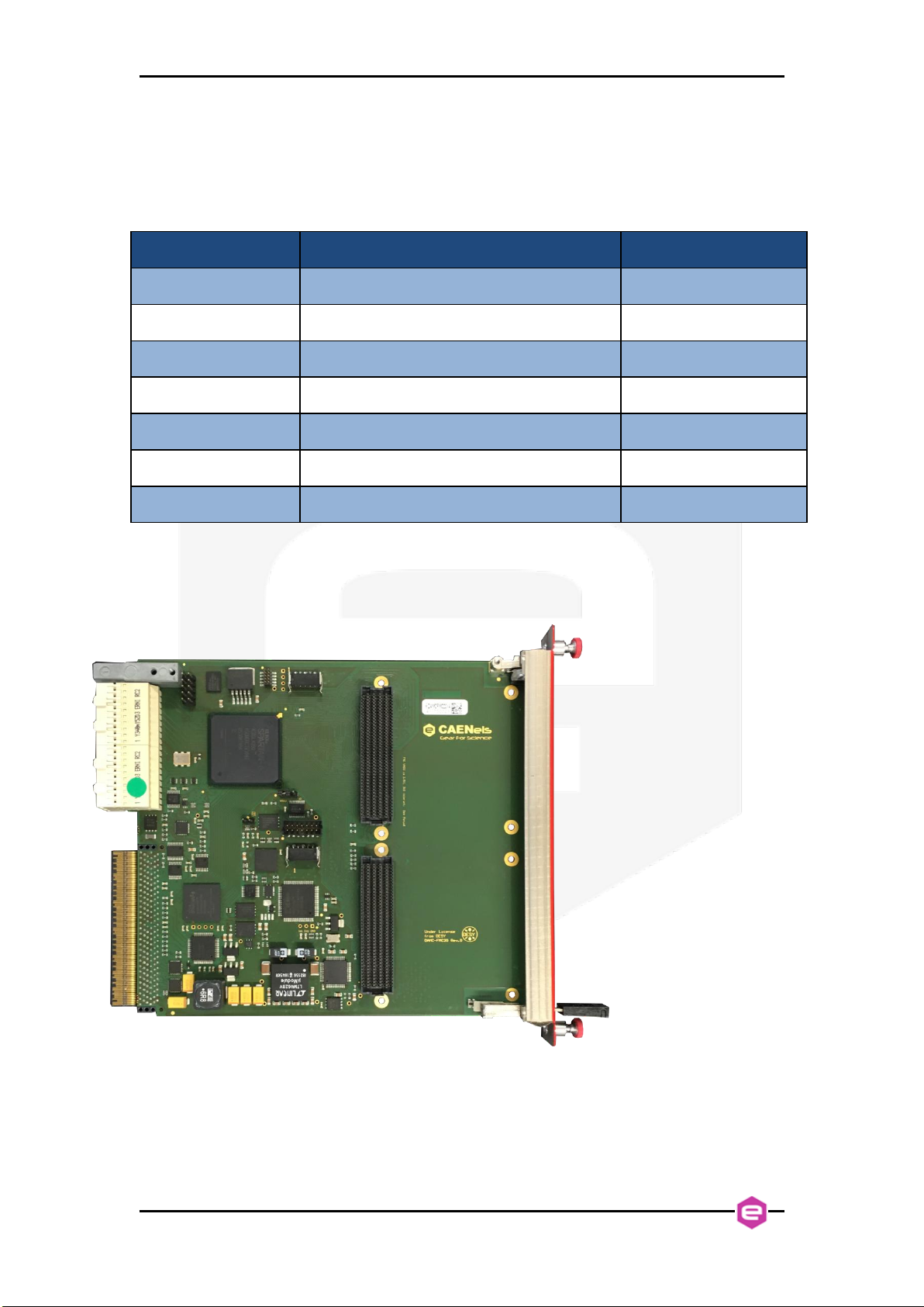
1.1 DAMC-FMC20 DESCRIPTION........................................................................8
1.2 DAMC-FMC20 OVERVIEW .........................................................................10
2. DAMC-FMC20 ARCHITECTURE.................................................................11
2.1 CLOCK TREE .................................................................................................12
2.2 JTAG CHAIN ................................................................................................14
2.3 FLASH PROGRAMMING................................................................................15
2.4 MODULE MANAGEMENT...............................................................................15
2.4.1 On-board Diagnostics..............................................................................16
2.4.2 On-board Voltage Monitoring and Implemented Functions ...................16
2.4.3 I2C Buses .................................................................................................17
2.4.1 AMC Connectivity....................................................................................17
2.5 RTM CONNECTOR ........................................................................................18
2.5.1 Zone 3 Class Compatibility......................................................................20
2.6 FMC CONNECTORS.......................................................................................21
2.6.1 FMC Connectors Remarks.......................................................................21
2.7 LED INDICATORS..........................................................................................21
2.8 MGT ROUTING AND CROSSPOINT SWITCH ...................................................22
2.9 POWER SUPPLY ARCHITECTURE ...................................................................23
2.10 CONNECTOR PIN ASSIGNMENTS....................................................................24
2.10.1 FMC Power Connector........................................................................24
2.10.2 JTAG Connector ..................................................................................24
2.10.3 Atmel Programmer Connector.............................................................25
2.10.4 RTM connector.....................................................................................25
2.10.5 AMC Connector Pin Assignment.........................................................27
2.10.6 FMC Low Pin Count (LPC) connector................................................28
2.10.7 FMC High Pin Count (HPC) Connector.............................................29
2.11 PINOUT FOR FPGAS......................................................................................31
2.11.1 UCF for Main FPGA...........................................................................31
2.11.2 UCF for Transceiver FPGA.................................................................45
3. REFERENCE FIRMWARE.............................................................................49
4. TECHNICAL SPECIFICATIONS ..................................................................51

DAMC-FMC20 User’s Manual
4
Document Revisions
Document Revision
Date
Comment
1.0
June 25th, 2019
First Release

DAMC-FMC20 User’s Manual
5
Safety information - Warnings
CAEN ELS will repair or replace any product within the guarantee period if
the Guarantor declares that the product is defective due to workmanship or materials
and has not been caused by mishandling, negligence on behalf of the User, accident or
any abnormal conditions or operations.
Please read carefully the manual before operating any part of the instrument
WARNING
Do NOT open the boxes
CAEN ELS s.r.l. declines all responsibility for damages or injuries caused
by an improper use of the Modules due to negligence on behalf of the User. It is
strongly recommended to read thoroughly this User's Manual before any kind of
operation.
CAEN ELS s.r.l. reserves the right to change partially or entirely the contents of this
Manual at any time and without giving any notice.
Disposal of the Product
The product must never be dumped in the Municipal Waste. Please check your local
regulations for disposal of electronics products.

DAMC-FMC20 User’s Manual
6
Read over the instruction manual carefully before using the instrument.
The following precautions should be strictly observed before using the device:
WARNING
Do not use this product in any manner not
specified by the manufacturer. The protective
features of this product may be impaired if it is
used in a manner not specified in this manual.
Do not use the device if it is damaged. Before
you use the device, inspect the instrument for
possible cracks or breaks before each use.
Do not operate the device around explosives gas,
vapor or dust.
Always use the device with the cables provided.
Turn off the device before establishing any
connection.
Do not operate the device with the cover
removed or loosened.
Do not install substitute parts or perform any
unauthorized modification to the product.
Return the product to the manufacturer for
service and repair to ensure that safety features
are maintained
CAUTION
This instrument is designed for indoor use and in
area with low condensation.

DAMC-FMC20 User’s Manual
7
The following table shows the general environmental requirements for a correct
operation of the instrument:
Environmental Conditions
Requirements
Operating Temperature
0°C to 50°C
Operating Humidity
30% to 85% RH (non-condensing)
Storage Temperature
-10°C to 60°C
Storage Humidity
5% to 90% RH (non-condensing)
This manual refers to the following boards:
-DAMCFMC20XAA - Dual FMC Carrier Board - MTCA.4 - Dual-FPGA
Processing

DAMC-FMC20 User’s Manual
8
1.Introduction
This chapter describes the general characteristics and main features of the
DAMC-FMC20 board.
1.1 DAMC-FMC20 Description
The DAMC-FMC20 is a cost-efficient FPGA mezzanine card (FMC) carrier
designed according to MTCA.4, it is equipped with two Spartan-6 FPGAs and it
simultaneously supports one low pin count and one high pin count FMC module.
While one FPGA allows serial high-speed communication (PCIe, RTM,
Backplane, FMCs), the other one allows implementing large signal processing
algorithms. The carrier supports one serial link (GTP) for HPC FMC module and up
to two serial links for LPC FMC module.
In addition, an extra 12V power connector for high current FMC applications is
foreseen for each FMC module.
The carrier provides one PCIe link that is AMC.1 type 1 compliant; the carrier
is also software-reconfigurable over PCIe and MMC. The AMC ports 12-15 are
connected via cross-point switch to the transceiver FPGA.
The board is a cost-effective approach for basic IO without high-demanding
computing requirements; an additional USB connection is optional for direct
debugging the FPGAs and MMC at the front panel.
The carrier management is compliant to the latest recommendation MMC V1.0.
The carrier Zone 3 is compliant to the Class D1.0.
The board provides the following features:
Double width, mid-size MTCA.4 form factor Advanced Mezzanine
Card (AMC)
Dual-FPGA processing
Xilinx XC6SLX45T for serial communication including PCIe
(transceiver FPGA)

DAMC-FMC20 User’s Manual
9
Xilinx XC6SLX150 for signal processing and connectivity to RTM
and FMCs (main FPGA)
Rear IO connected to FPGA, Class D1.0 compatible
Supports 2 FMCs: One HPC module and one LPC module
Front panel with hot-plug switch, mandatory LEDs required by IPMI
standard and four additional LEDs
USB debug interface at front panel for FPGAs and MMC controller
Remote configurable over PCIe, MMC or download cable
ANSI/VITA 57.1 compliant
Extra power connector for booth FMCs
IPMI 1.1 compliant MMC
RoHS compliant

DAMC-FMC20 User’s Manual
10
1.2 DAMC-FMC20 Overview
The DAMC-FMC20 main components are listed in the below table:
Component
Purpose
Manufacturer
XC6SLX150-3FG900I
Main FPGA
Xilinx
XC6SLX45T-2CSG324I
Transceiver FPGA (PCIe bridge and MGT)
Xilinx
SN65LVCP408
8x8 crosspoint switch
Texas Instruments
ICS874003
PCIe jitter attenuator
Intersil
FT4232H
Hi-speed quad USB UART IC
FTDI
ATxmega128A1
MMC controller
Atmel
TPS2458
Hotswap controller, load current monitor
Texas Instruments
Such components are placed on the board as in the picture below:
1Main FPGA XC6SLX150
2HPC FMC power output
connector
3LPC FMC power output
connector
4JTAG connector
5FMC HPC connector
6FMC LPC connector
7USB connector
8AMC connector
9Transceiver FPGA
XC6LX45T
10 Cross-point switch
11 MMC ATxmega128A1
12 2 SPI FLASH ICs
13 XC6LX150 Platform
FLASH
14 RTM connector

DAMC-FMC20 User’s Manual
11
2.DAMC-FMC20 Architecture
In this chapter a deep technical overview of the DAMC-FMC 20 board is given;
the basic block diagram is presented below:
The transceiver FPGA provides control over PCIe and processes all serial links. It
is connected to the main FPGA through a 64 bit parallel chip-to-chip interface;
furthermore, both FPGAs are connected via four LVDS lanes.
Note that Xilinx Spartan only supports LVDS driver on Bank 0 and on Bank 2,
this limiting the number of pins that are available for bidirectional LVDS
communication. DAMC-FMC20 pin assignment allows all LVDS pins on RTM and
full bidirectional LVDS on LPC.

DAMC-FMC20 User’s Manual
12
On HPC FMC, while the LPC pins (36 lanes) can operate in bidirectional mode,
the additional HPC pins (40 lanes) are input-only LVDS.
If outputs on these pins are desired, other standards such as LVCMOS25 must be
used.
2.1 Clock Tree
The DAMC-FMC20 has a flexible clock tree, since FPGA global clocks can be
accessed from PCIe clock as well as from TCLKA or TCLKB. Furthermore, local 200
MHz oscillators are present for booth FPGAs.
A clock from RTM is fed to the main FPGA and to the transceiver FPGA. A
multiplexer selects if TCLKA or TCLKB are output to RTM.
The clock tree diagram is presented below:
PLL
PCIe Clk
Buffer
PCIe Clk x 2.5
PCIe Clk x 2.5
PCIe Clk x 2.5
TCLKA
Buffer
TCLKB
TCLKA
TCLKA
TCLKB
TCLKB
TCLKA
XC6SLX150
XC6SLX45T
GC
GC
RTM
GC
RTM_CLK
GC
TCLKA or TCLKB
GC
TCLKA
TCLKA
TCLKB
RTM_CLK
TCLKB
GC
GC
From CPLD
(50 MHz div 1..16)
MUX
TCLKB
RTM Clocks
PCIe Clk x 2.5
PCIe Clk x 2.5
FMC
HPC
FMC
LPC
MGT101CLK PCIe Clk x 2.5
GBTCLK0_M2C
GBTCLK0_M2C
RTM_CLK
125
MHz
LVDS
RTM/ 125MHz
MGT123CLK
GC
AMC_CLK
From CPLD
(50 MHz div 1..16)
The clock tree provides following features:
Distribution of PCI clock (multiplied by factor 2.5) to transceiver FPGA GTP
block, transceiver FPGA global clock and main FPGA global clock;
Distribution of TCLKA to transceiver FPGA global clock, main FPGA global
clock and RTM (multiplexed with TCLKB);

DAMC-FMC20 User’s Manual
13
Distribution of TCLKB to main FPGA global clock and RTM (multiplexed
with TCLKA);
Distribution of RTM clock to main FPGA global clock and transceiver FPGA
(MGT clock);
Two clock sources for first MGT tile on transceiver FPGA: PCIe clock and
FMC clock;
Two clock sources for second MGT tile on transceiver FPGA: FMC clock and
(as a placement option) RTM clock or 125 MHz fixed LVDS clock;
200 MHz LVDS clock source for each FPGA as global clock.

DAMC-FMC20 User’s Manual
14
2.2 JTAG Chain
The DAMC-FMC20 is provided with a high-flexibility JTAG chain, which can
be routed to Xilinx Platform Cable connector, Soft-JTAG over USB (FTDI MPSSE)
or AMC connector.
A CPLD that is controlled over MMC’s IPMI or over MMCs UART debug
interface (over USB) selects the configuration of the chain, which contains the
transceiver FPGA by default.
Optionally, main FPGA with dedicated Platform FLASH, RTM and/ or booth
FMCs can be included in the chain.
Below a schematic of the chain is presented:
SPI
FLASH
14-pin
connector MUX
Xilinx
PF
Cable
Spartan-6
LX45T
MMC V1.0
Atxmega
128
CPLD
SPI
FLASH
RTM
JTAG
10-pin
connector
Jumper
PDI
AMC
JTAG
SPI
Control
SPI
PCIe
FMC1
JTAG
FMC2
JTAG
SPI
Programming
Control
(Prog_B, Init,
Done, …)
Atmel
Programmer
JTAG
RTM
JTAG
Spartan-6
LX150
USB
JTAG Player*
Soft JTAG*
* lines are shared for
SPI and soft JTAG/
JTAG player
FTDI
MPSSE
engine
JTAG
SPI
FLASH
SPI
Program
ming
Redundant
The chain provides following features:
JTAG input from 14-pin connector, AMC, soft JTAG player (in MMC or
transceiver FPGA);
JTAG output to transceiver FPGA and main FPGA (including Platform
FLASH);
Extended JTAG output to RTM, FMC1 and FMC2;
Controlled over Xilinx CoolRunner-II CPLD (code based on DESY MMC
V1.0 reference design);
JTAG chain configuration over IPMI interface on MMC or over UART
interface on MMC.

DAMC-FMC20 User’s Manual
15
2.3 FLASH Programming
Following ways exist to program the on-board FLASH memories:
MMC Atmel ATxmega 128A1 (integrated FLASH memory)
Programming with programming cable using 6-pin Atmel PDI connector;
In-crate programming using HPM1.*
FPGAs (2 SPI FLASH memories)
Programming using Xilinx Platform Cable;
Programming over AMC backplane or USB* (MPSSE);
Programming over PCIe-to-SPI Interface (supported by Reference BSP);
Direct SPI Programming over IPMI (programming of 2 images; supported by
MMC V1.0 reference code).
RTM, FMC1, FMC2
Programming using programmer on 14-pin connector;
Programming over AMC backplane or USB* (MPSSE);
Programming using JTAG player in transceiver FPGA;
Programming over JTAG player* in MMC.
* software support not included yet
2.4 Module Management
The MMC is implemented in an ATxmega128A1 microcontroller. The IPMI
protocol is compliant to IPMI 1.1 standard, RTM and FMCs have separate I2C
connections to the microcontroller.
The MMC has an additional EEPROM for configuration purposes and a
temperature sensor for measuring the cooling performance in the uTCA crate. The

DAMC-FMC20 User’s Manual
16
hot-plug switch and LEDs required by IPMI standard are present, while an optional
USB connector is present at the front panel for debugging the controller.
The programming of the microcontroller is done through a direct SPI connection
or the common JTAG chain of the board.
2.4.1 On-board Diagnostics
The board contains an optional FT4232 four-channel USB bridge chip, and the
two Xilinx FPGAs, the MMC and the JTAG interface are connected to each of its
channels for debugging and monitoring. A temperature sensor and monitoring
capability of all supply voltages is implemented in the MMC using ADCs, while four
LEDs at the front panel show user defined status of the FPGAs.
2.4.2 On-board Voltage Monitoring and Implemented Functions
The DAMC-FMC20 follows the MMC V1.0 recommendation, following voltages
can be monitored:
Monitoring of 1.2V GTP;
1.2V FPGA core voltage (main and transceiver FPGA);
1.8V monitoring;
2.5V monitoring;
3.3V monitoring;
3.3V management power monitoring;
12V payload power monitoring;
RTM power and current measurement: Power to RTM Interface (12V and
3V3) is controlled by MMC via dedicated power switch. Current consumption
is monitored via ATxmega analog inputs).
The following functions are supported:
Hot-swap handle control;
Regulator power good monitoring;
FMC power good monitoring;
FMC present monitoring;

DAMC-FMC20 User’s Manual
17
UART debug interface (over UART-to-USB translator);
Transceiver FPGA SPI FLASH programming (2 memories);
Transceiver FPGA control (reset, reboot etc.).
2.4.3 I2C Buses
MMC on DAMC-FMC20 has four independent I2C buses: Bus one is connected
to the AMC interface (IPMI-B), Bus two is connected to the RTM using an I2C
isolator and Bus three is connected to on-board sensors. Addresses are: 0x51 for serial
number IC, 0x38 for I2C expander and 0x49 for temperature monitor.
A schematic is presented below:
MMC V1.0
Atxmega
128
FMC1
JTAG
FMC2
JTAG
AMC Connector
Bus 1
Bus 3Bus 4
Serial
Number
+
2KB EEPROM
I2C
Expander
Temp.
Monitor
Bus 2
RTM Connector
Address:
101.0001
Address:
011.1000
Address:
100.1001
I2C
Isolator
2.4.1 AMC Connectivity
Available connections are presented in the below table:
Channel
Signal
Voltage levels
Protocol/Signal
Remarks
4
PCIe x1 (lane 0)
CML
AMC.1
PCIe Bus
12
cross point switch
CML
custom
RIO (Xilinx)
13
cross point switch
CML
custom
RIO (Xilinx)
14
cross point switch
CML
custom
RIO (Xilinx)

DAMC-FMC20 User’s Manual
18
15
cross point switch
CML
custom
RIO (Xilinx)
17_RxD
TRGSTART
MLVDS
custom
bidirectional
17_TxD
TRGEND
MLVDS
custom
bidirectional
18_RxD
TRGREADOUT
MLVDS
custom
bidirectional
18_TxD
CLK_AUX
MLVDS
custom
bidirectional
19_RxD
RESET
MLVDS
custom
bidirectional
19_TxD
INTERLOCK0
MLVDS
custom
bidirectional
20_RxD
INTERLOCK1
MLVDS
custom
bidirectional
20_TxD
INTERLOCK2
MLVDS
custom
bidirectional
TCLKA
f = 108 MHz
LVDS - terminated
fast clk
input
TCLKB
f = 4.514 MHz
LVDS - terminated
slow clk
input
FCLKA
f = 100 MHz
LVDS
sclock for PCIe
input
JTAG
JTAG
LVCMOS (3.3 V)
JTAG chain
IPMI
IPMI
LVCMOS (3.3 V)
IPMI for MMC (SCL/SDA)
with pull-up
PS
PS0, PS1
LVCMOS (3.3 V)
presence detect
with pull-up
GA
GA0/GA1/GA2
LVCMOS (3.3 V)
geographical address
pull-up by MMC
Enable_n
Enable_n
LVCMOS (3.3 V)
enable
with pull-up
MP +3V3
MP +3V3
Power supply
management power
0,15 A/150 uF
PP +12V
PP +12V
Power supply
payload power
7,4 A/800 uF
2.5 RTM Connector
The Z3 RTM connector carries following electrical signals (according to Class
D1.0):
AMC clock (global clock from main FPGA going to AMC)
TCLKA or TCLKB (clock from AMC to RTM)
RTM present signal
RTM I2C (isolated, control from MMC)
RTM clock (clock from RTM going to AMC)
JTAG interface (connected to CPLD)
Bidirectional LVDS bus (connected to 2.5V FPGA bank)

DAMC-FMC20 User’s Manual
19
3V3 management power (switched through MMC)
12V payload power (switched through MMC)

DAMC-FMC20 User’s Manual
20
2.5.1 Zone 3 Class Compatibility
The connector is compatible to the double row B+ connector specified in
Advanced Mezzanine Card Base Specification; the connectivity of signals is based on
the PICMG MTCA.4 RI.0 draft 0.7d specification (Revision 1.0 Draft 0.1p4).
The Zone 3 connector (J30) is compliant to Class D1.0 (54 LVDS I/O signals;
LVDS 2.5V). All IO lines are connected to differential IO pins of the XC6SLX150
Spartan-6 FPGA as reported in the tables below:
a
b
c
d
e
f
1
PWR+12V
PWR+12V
PS#
SDA
RTM_TCK
RTM_TDO
2
PWR+12V
PWR+12V
MP+3.3V
SCL
RTM_TDI
RTM_TMS
3
P30_IO+
P30_IO-
P30_IO+
P30_IO-
P30_IO+
P30_IO-
4
P30_IO+
P30_IO-
P30_IO+
P30_IO-
P30_IO+
P30_IO-
5
P30_IO+
P30_IO-
P30_IO+
P30_IO-
P30_IO+
P30_IO-
6
P30_IO+
P30_IO-
P30_IO+
P30_IO-
P30_IO+
P30_IO-
7
P30_IO+
P30_IO-
P30_IO+
P30_IO-
P30_IO+
P30_IO-
8
P30_IO+
P30_IO-
P30_IO+
P30_IO-
P30_IO+
P30_IO-
9
P30_IO+
P30_IO-
P30_IO+
P30_IO-
P30_IO+
P30_IO-
10
P30_IO+
P30_IO-
P30_IO+
P30_IO-
P30_IO+
P30_IO
Table 1: AMC Z3 J30 pin assignment for Class D1.0
a
b
c
d
e
f
1
P31_IO+
P31_IO-
P31_IO+
P31_IO-
P31_IO+
P31_IO-
2
P31_IO+
P31_IO-
P31_IO+
P31_IO-
P31_IO+
P31_IO-
3
P31_IO+
P31_IO-
P31_IO+
P31_IO-
P31_IO+
P31_IO-
4
P31_IO+
P31_IO-
P31_IO+
P31_IO-
P31_IO+
P31_IO-
5
P31_IO+
P31_IO-
P31_IO+
P31_IO-
P31_IO+
P31_IO-
6
P31_IO+
P31_IO-
P31_IO+
P31_IO-
P31_IO+
P31_IO-
7
P31_IO+
P31_IO-
P31_IO+
P31_IO-
P31_IO+
P31_IO-
8
P31_IO+
P31_IO-
P31_IO+
P31_IO-
P31_IO+
P31_IO-
9
P31_IO+
P31_IO-
P31_IO+
P31_IO-
P31_IO+
P31_IO-
10
P31_IO+
P31_IO-
P31_IO+
P31_IO-
P31_IO+
P31_IO-
Table 2: AMC Z3 J31 pin assignment for Class D1.0
Table of contents
Other Caen ELS Carrier Board manuals