Casio UP-400 User manual

SERVICE MANUAL
UP-400
NOV. 2008
INDEX

CONTENTS
UP-400 PAGE
1. SPECIFICATIONS
1-1. PRINTING SPECIFICATION ..............................................................................1
1-2. PAPER SPECIFICATION ...................................................................................1
1-3. INTERFACE SPECIFICATION ..........................................................................2
2. DISASSEMBLY .............................................................................................4
3. CIRCUITRY
3-1. POWER SUPPLY CIRCUIT ...............................................................................7
4. MAINTERNANCE & TROUBLESHOOTING
4-1. INSTALLING OR REPLACING PAPER ROLL .................................................8
4-2. ADJUSTING THE PAPER NEAR END SENSOR .............................................8
4-3. PAPER JAM .......................................................................................................9
4-4. TROUBLESHOOTING .....................................................................................10
4-5. SELF TEST ...................................................................................................... 11
5. SETTING & CHECKING THE DIP SWITCHES .......................................... 12
6. CIRCUIT DIAGRAMS ..................................................................................14
7. PARTS LIST ................................................................................................18

– 1 –
1. SPECIFICATIONS
1-1. PRINTING SPECIFICATION
Printing method: Direct Line Thermal
Dot pitch: 8 dot / mm
Printing speed: 210 mm per second (Max.)
Printing width: 72mm / 576 dots
Character structure: 8 x 16 (font B) 12 x 24 (font A)
Printing columns: 64 columns / line 44 columns / line
Character size: 1.00 x 2.00 1.50 x 3.00
Fonts: US-ASCII, Katakana, international characters
Feed speed: 220 mm per second
Interface: RS232C (serial), 10/100 Base - T/ TX
Command: ESC / POS compliant
Paper width & diameter: 80 mm (W) x 80 mm Dia. Max.
Thermal head life: 100 Million Pulses / 100 km or more
Cutting method: *2 Partial cut (one point left uncut) *2
Operating temperature: 5 °C ~ 35 °C
Storage temperature: -20 °C ~ 60 °C
Dimension: 145 mm (W) x 193.2 mm (L) x 120.1 mm (H)
Transfer speed: 38.4 kBps (Max.) : RS-232C
Supply voltage in standby: 24V DC / 100mA
Mean current: Approx. 1.3 A *3
Power consumption: Approx. 40 W *3
Weight: 1.1kg
Barcode alignment: ○
Near end sensor: Near end sensor
*1 Manufactured by SIIP&S Inc. (Former name: Seiko Instruments Inc.)
*2 CAUTION: Paper must be fed 3 mm after cutting to prevent paper jam.
*3 These values vary according to environmental temperature when printed font A (12 × 24) with a rolling
pattern.
1-2. PAPER SPECIFICATION
Paper Width: 79.5 ± 0.5mm (3.13 ± 0.02”)
Paper roll size: Roll diameter: Maximum 80 mm (3.15”)
Take-up paper roll width: 80 + 0.5/-1.0mm (3.15 + 0.02/-0.04”)
Specified paper: Specified thermal roll paper: NTP080-80
[Paper:TF50KS-E2C Nippon Paper Industries Co., Ltd.]
Packaged roll paper:
[Paper:PD160R-N (Oji Paper Mfg. Co., Ltd.)]
*The following paper can be used instead of the paper above:
Paper: HP220AB1 (Mitsubishi Paper Mills Ltd.)
Paper roll spool diameter: Inside 12 mm (0.47”)
Outside 18 mm (0.71”)
NOTE: The end of the paper roll must be free to come off the spool when finished. It must not be adhesively
attached or attached in another semi-permanent manner.

– 2 –
1-3. INTERFACE SPECIFICATION
1-3-1. RS-232C SPECIFI CATION
Data transmission: Serial. EIA RS232C compliant
Synchronization: Asynchronous
Handshaking: DTR/DSR or XON/XOFF control (*)
Signal levels: MARK = -3 to -15V: Logic “1”/OFF
SPACE = +3 to +15V: Logic “0”/ON
Baud rate: 4800, 9600, 19200, 38400 bps (*)
Data word length: 8 bits, 7 bits (*)
Parity Settings: None, even, odd (*)
Stop bits: 1 or more
Connector (printer side): Male DSUB-9 pin connector
Notes: *The data word length, baud rate, and parity depend on the DIP switch settings. (Refer to
5.SETTING & CHECKING THE DIP SWITCHES.)
1-3-2. RS-232C INTERFACE CONNECTION EXAMPLE
HOST SIDE PRINTER SIDE
(DTE ex.8251) (Pin No.)
TxD RxD (2)
RxD TxD (3)
DTR DSR (6)
DSR DTR (4)
RTS
CTS
GND GND (5)
1-3-3. LAN CONNECTOR
PIN DESCRIPTION
1 TX+
2 TX-
3 RX+
4 Isolated GND
5 Isolated GND
6 RX-
7 Isolated GND
8 Isolated GND
1-3-4. POWER SUPPLY CONNECTOR
The connector is connected the printer to an external power source.
CONNECTOR MODEL:
PIN SIGNAL
1 +24V
2 GND
3 NC
shell FG
18
Shell
1
2
3

– 3 –
1-3-5. DRAWER KICK-OUT CONNECTOR
The pulse specified by ESC p or DLE DC4 is output to this connector. The HOST can confirm the
status of the input signal by using the DLE EOT, GS a, or GS r commands.
PIN I/O DESCIPTION
1 - Frame ground
2 Output Drawer kick-out drive signal 1
3 Input Drawer open/close signal
4 Output +24 V
5 Output Drawer kick-out signal 2 *
6 - Signal ground
CONNECTIOR MODEL:
Printer side: MOLEX52065-6615 or equivalent
Used side: 6-position 6-contact (RJ12 telephone jack)
* Two drawers can be used with a Y-cable that meets the following specifications.
Pin 1: Frame ground .............................................................Pin1
Pin 2: Drawer kick-out drive signal 1 .....................................Pin2
Pin 3: Drawer open/close signal ............................................Pin3 Connector of Drawer No.1
Pin 4: +24V ..........................................................................Pin4
Pin 5: Drawer kick-out signal 2 .................... ..........Pin6
Pin 6: Signal ground Pin6 ............. ..............................Pin1
........................Pin2
...................Pin3 Connector of Drawer No.2
..............Pin4
........................................Pin6
1 6

– 4 –
2. DISASSEMBLY
1. Remove four screws at the bottom of the printer unit.
2. Remove five connectors (CN1, CN2, CN3, CN5, CN6) and the FFC (J1).
Screws
CN3
CN2 J1
CN1
CN5
CN6
3. Remove three screws and then remove the main PCB.
Screws

– 5 –
Precaution when assembling:
Let the connector through the hole.
Precaution when assembling:
Slide the lever of the cover to “close” and then fit the
upper cover into the printer.
4. Remove two screws.
5. Remove the upper cover while the printer cover is open.
Screws
7. Remove two screws and then the control panel.
Screws
6. Remove the screw and then the printer cover.
Screw

– 6 –
8. Remove the two screws and then the paper guide and the cutter.
Screws
10. Remove the four screws and then the printer unit.
9. Remove the power switch.
Screws
Screws
11. Loosen the two screws and then remove the end sensor unit.
Precaution when assembling
Fix the end sensor unit at the lowest of the groove.
Loosen
Precaution when assembling:

– 7 –
3. CIRCUITRY
3-1. POWER SUPPLY CIRCUIT
The power supply source is a DC 24V.
AC
ADAPTOR
CPU
VCC3
ROM
RAM
U1
U2
U3. 21
U13
U14
DRIVER
DRIVER
DC24V
POWER SW U18 U19
U11
VP(+24V)
Q5
FET
VP
HVP
VCC
VCC
VCC
VCC
VP
AUTO
CUTTER
PRINTER
MOTOR
PRINTER
HEAD
BUFFER
LATCH
U7
LED DS1
VCC3
VCC3
VCC3
OTHER IC
REGULATOR REGULATOR
VCC(+5V) VCC3 (+3.3V)
– 8 –
4. MAINTERNANCE & TROUBLESHOOTING
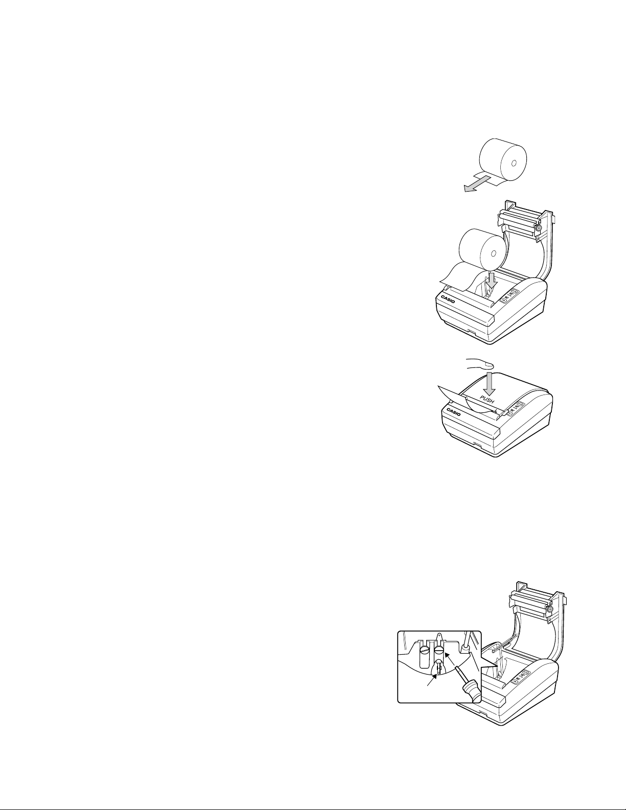
4-1. INSTALLING OR REPLACING PAPER ROLL
CAUTION: Make sure that paper rolls meets printer’s specifi cation. Do not use paper rolls that have one
end glued to the core. This causes excessive load on the paper feed.
1: Make sure that the printer is not printing or receiving data, and open the
printer cover by sliding the cover open knob. Unroll 10 to 15 cm of the
paper as shown.
2: Insert the paper roll as shown.
3: Pull out 10 to 15 cm of paper and close the printer cover as shown.
Tear off the excess paper on the cutter edge.
4-2. ADJUSTING THE PAPER NEAR END SENSOR
A sensor detects when the paper roll is running out. Due to variation in the width of paper roll cores, it is
diffi cult to measure the exact length of the paper left on the roll when the detector is triggered. The factory
setting is based on a paper roll core with an outside diameter of 18 mm and an inside diameter of 12 mm. If
you use a paper roll with different widths, adjust the setting as described below.
1: Open the printer cover and remove the paper roll.
2: Loosen the adjusting screw and move the tab to fit the core of the paper roll.
3: Tighten the adjusting screw.
4: Replace the paper roll and close the printer cover.
Tab
Table of contents
Other Casio Printer manuals

Casio
Casio UP-250 User manual

Casio
Casio CW-50 - Disc Title Printer Color Thermal... User manual

Casio
Casio UP-250 User manual

Casio
Casio M-U420 User manual

Casio
Casio MD-910 User manual

Casio
Casio IT-3000 - Win CE .NET 4.1 400 MHz User manual

Casio
Casio IT-9000 Series User manual

Casio
Casio UP-370 User manual

Casio
Casio M-U420 User manual

Casio
Casio KL-G2 User manual

Casio
Casio KL-G2TC User manual

Casio
Casio SP-1300 User manual

Casio
Casio FP-12 User manual

Casio
Casio CW-E60 - Disc Title Printer B/W Thermal... User manual

Casio
Casio IT-3000 Series User manual

Casio
Casio J20 User manual

Casio
Casio RJA514733-9 User guide

Casio
Casio UP-360 User manual

Casio
Casio MEP-U10 User manual


