Casio QW-2741 User manual

SERVICE MANUAL
& PARTS LIST
(WITHOUT PRICE)
QW-2741
MODULE NO.
R
REF. NO. S/M-808
APR. 2003
WVA-310DQ

CONTENTS
1. SPECIFICATIONS: MODULE QW-2741 .................................................... 1
2. DRAWINGS: MODULE QW-2741
2-1. LCD DIAGRAM ............................................................................................. 2
2-2. CIRCUIT DIAGRAM ...................................................................................... 3
2-3. CHECKING TERMINALS AND COMPONENTS ..........................................4
2-4. P1 ~ P5 PADS ...............................................................................................4
3. EXPLODED VIEW: MODULE QW-2741 .................................................... 5
4. PARTS LIST: MODULE QW-2741 ............................................................. 6
5. PRECAUTIONS FOR REPAIR: MODULE QW-2741
5-1. AC (ALL CLEAR) AND REMOVING OF MODULE ...................................... 7
5-2. ACCURACY CHECKING .............................................................................. 7
6. TROUBLESHOOTING FOR TIME RECEPTION: MODULE QW-2741 ..... 8

— 1 —
1. SPECIFICATIONS: MODULE QW-2741
Battery CTL1616 (Storage battery)
Note: Use CTL1616 only. Other storage battery or CR1616 can cause
damage to the watch.
Battery life Approx. 6 month (from full charged condition)
Current consumption 0.548 µA maximum
Alarm system Piezo plate on Cover/Back
Accuracy ±15 sec./month
Accuracy setting system Trimmer capacitor
Accuracy checking See page 7
Functions • Electro-luminescent backlight
Afterglow
• Solar powered
• Time calibration signal reception
Auto receive (Twice a day, at 2:00 AM, 4:00 AM)
Manual receive
Last date/time received display
• Time Calibration Signal
Station name: JJY (Fukuoka/Saga, Japan)
Frequency: 60 kHz
Range: Approx. 1,000 km
• 20 Telememo pages
8 letters and 12 numbers per page
Others: Auto-sort, remaining memory
• World Time
29 time zones (28 cities), daylight saving time on/off
• Day Counter
Automatically counts down the days from the current date to a target date.
Memory capacity: 5records (8 characters of text)
• 1/100-sec. stopwatch
Measuring capacity: 23:59’59.99"
Measuring modes: Elapsed time, split time, 1st-2nd place times
• Daily alarms
3 independent daily alarms
• Hourly time signal
• Low battery warning display
• Auto-calendar (to year 2039)
• 12/24-hour format
• Regular timekeeping:
Analog: 2 hands (Hr, min.)
Digital: Hr, min, sec, pm, month, date, day
Item Detail

— 2 —
2. DRAWINGS: MODULE QW-2741
2-1. LCD DIAGRAM
SEG. COM.
L 1
L 2
L 3
L 4
L 5
L 6
L 7
L 8
L 9
L10
L11
L12
L13
L14
L15
L16
L17
L18
L19
L20
L21
L22
L23
L24
L25
L26
L27
L28
SDS
LC1
BAT0
X0Y4
X1Y4
X2Y4
X3Y4
X4Y4
DST
e3
d3
c3
e2
d2
c2
X5Y4
X6Y4
X7Y4
X8Y4
X9Y4
X18Y4
X17Y4
X16Y4
X15Y4
X14Y4
X13Y4
X12Y4
X11Y4
X10Y4
LC2
BAT1
X0Y3
X1Y3
X2Y3
X3Y3
X4Y3
c0
d0
e0
c1
d1
e1
COL
X5Y3
X6Y3
X7Y3
X8Y3
X9Y3
X18Y3
X17Y3
X16Y3
X15Y3
X14Y3
X13Y3
X12Y3
X11Y3
X10Y3
ANT2
LC3
ALM
X0Y2
X1Y2
X2Y2
X3Y2
X4Y2
b0
g0
f0
b1
g1
f1
HYP
X5Y2
X6Y2
X7Y2
X8Y2
X9Y2
X18Y2
X17Y2
X16Y2
X15Y2
X14Y2
X13Y2
X12Y2
X11Y2
X10Y2
ANT1
LC4
SIG
X0Y1
X1Y1
X2Y1
X3Y1
X4Y1
PM
a0
a3
a1
a2
X5Y1
X6Y1
X7Y1
X8Y1
X9Y1
X18Y1
X17Y1
X16Y1
X15Y1
X14Y1
X13Y1
X12Y1
X11Y1
X10Y1
ANT0
LC5
RECOVER
X0Y0
X1Y0
X2Y0
X3Y0
X4Y0
24H
f3
g3
b3
f2
g2
b2
X5Y0
X6Y0
X7Y0
X8Y0
X9Y0
X18Y0
X17Y0
X16Y0
X15Y0
X14Y0
X13Y0
X12Y0
X11Y0
X10Y0
SDC
CHARGE
L18
L1
L2
L3
L4
L5
L6
L7
L8
L9
L10
L11
L12
L13
L14
L15
L16
L17
L19
L20
L21
L22
L23
L24
L25
L26
L27
L28
SDS
SDC
LC1
LC2
LC3
LC4
LC5
PM
24H
a3
f3 b3
g3
e3 c3
d3
a2
f2 b2
g2
e2 c2
d2
COL
HYP
a1
f1 b1
g1
e1 c1
d1
a0
f0 b0
g0
e0 c0
d0
X0 X18
Y0
Y4
ALM
SIG
DST
CHARGE BAT0 BAT1 RECOVER
ANT0
ANT1
ANT2

—3 —
2-2. CIRCUIT DIAGRAM
✽ 1.No bonding
✽ 2.Short (Soldering) (Switching function)
KI6: Open (No Soldering)
KI7: Open (No Soldering)
KI8: Open (No Soldering)
✽ 3. Latch Type Key
✽ 4.Short (Soldering)
✽ 5.Inclination sensor
Not mounted in this module.
✽ 6.Normal High for LD1
✽ 7.GNDB is used for the bias on the back of the tip.
✽ 8.Rant1 is not mounted in this module.
LSI
TOTAL 123PINS
BONDING 81PINS
LCD (2.8V 1/3b 1/5d)
INV
IC
L1 L28 L29 L61 LC1 LC5 SDS SDC
✽1✽1✽1✽1
GND VDD2
BAT
VCH VDD3 VC1 VC2
C1
C3C5
XTB
Xtal1
CT
LD1
S1
S2
S3
VDD1
C2
BD1
C8
LL1
Tr1
XT
T1
T2
T3
KI1
KI2
KI3
KI4
KI5
KI6
KI7
KI8
KI9
EMP ✽3
S4
SCR
SCIN
RP1RP2
Cp
PZ
VDSP
C4
VC3 VC4
Di1
V_TQ
C7
SDA SCL SCUT
AC
T4
D0
KC4
KC3
KC22
KC1
R1
R2
VSC
C6
SC
C9
CLF1
E’
Cel
EL LL2
L+
VOUT
L-
GND
CLF2
V+
BACK
FRONT
✽4
✽4
SL
PON
O1
O2
O4
O3
✽1
✽1
✽1
✽8
T5
R3
✽4
LD2 ✽1
✽3
✽3
✽3
✽3
✽3
✽3
✽1
VC5 VC6
✽1✽1
Z
SK
VPM RPM
1
Xtal2
ANT
Rxt2
Di2 R1
An.B
KS ✽5
Rb
GNDB
✽7
Rpd
Crh2
Crh1
Crh0
Rant2
Rant1
Creg
Cf12
Cagc
Cf13
Ccp9 Rcp
Cxt
Rxt1
Rbat Cbat
Crh3
✽2
✽2
✽2
16
215
314
413
512
611
710
8
IN1
IN2
VCC
OUT1
OUT2
GND
REC
DEC1
REG
PON
AGC
FIL1
FIL2
TCO
HOLD
DEC2 9

— 4 —
2-3. CHECKING TERMINALS AND COMPONENTS
Top view of P.C.B. ass'y Bottom view of P.C.B. ass'y
2-4. P1 ~ P5 PADS
Never solder or desolder these pads, because they have been selected best in the production line.
A new PCB ass'y as a spare parts will be supplied with factory adjustment of these pads.
3
VDD2
V_TQ
GND
VDSP
GND
VDD1
VDD3
GND
VC4
VC3
VPM
R1
R2
R3
16
1
DO
3
CLF1
CLF2 GND
L+
L-
VOUT
V+(VDD2)
LC5 LC4 LC3LC2LC1
LC5
LC4
LC3
LC2
AC
T1
T2T4
EMP
R1
R2
R3
XT
XTB
SCIN
SCR
VSC
VDD1
VDD3
VDSP
VC3
VC4
O2
O2
KI6 KI7KI8
KI8
KI7
KI6
D0
2
16
13
12
VPM
VOUT
VCH
BD1
KI9
KI1
KI4
KI2
KI2
KI3
V_TQ
KC4 KC3
16
14
R6
9
SL
KI5
GND GND
GND
GND
GND
VDD2
VDD2
GND
GND
GND
GND
L+
L-
KC1
KI9
CLF2CLF1
GND
GND
R6
GND
GND
VC1
VC2
GND
GND
LD1
L1
LC1
SDC
SDS
L28
L27
L26
L25
L24
L23
L22
L21
L20
L19
L18
L17
L16
L15
L14
L13
L12
L11
L10
L9
L8
L7
L6
L3
L2
KI2
T5
T3
PON
GND
L5
L4
LD1
GND
VDD2
GND
GND
GNDB GND
3
SCIN SCR
12
8
1
9
7
GND
VSC
L
VCH
VC1VC2
4
7
SCIN
SCIN
VSC
BD1
VDD2
7
AC
KC4
KC1
VCHKI9
KI9
5
KI2
KI3
KI1
KI4
VC1
VSC
GND
GND
GND
GND
GND
VDD2
GND
16
VDD2
VDD2
L
L
L
GND
GND
LD1
GND
5
4
2PON
D0
SL
12
13
14
XT
XT
XTB
02 D0
VDD2
KC3
VOUT
VDSP
R1
R1
R1
R4
R4
R7
R7
GNDB
KC1
GND
GND
KI8
GND
O1
Xtal2
Capacitor/Chip
Cbat
Capacitor/Chip
Ccp9
Resistor/Chip
Rpd
Capacitor/Chip
Cf12
Capacitor/Chip
Cf13
Capacitor/Chip
Cagc
Capacitor/Chip
Creg
Capacitor/
Chip
Cxt
Transistor
Tr1
Diode
Di2
Diode
Di1
Capacitor/
Chip
Cel
Resistor/Chip
RPM
Resistor/Chip
RP1
Resistor/
Chip
RP2
Coil
LL2
Coil
LL1
Inverter
INV
3. PCB ASS'Y
(7640 6705)
4. Capacitor/Trimmer
(1001 0950)
5. Oscillator/Crystal
(7110 6323)
Oscillator/Crystal
Xtal1
9. Cushion/506
(7211 9631)
Varistor
Z
Resistor/
Chip
Rb
Resistor/
Chip
R1
Detection IC
IC
Capacitor/Chip
C6 Capacitor/Chip
C4
Capacitor/Chip
C7
Capacitor/Chip
C8
Capacitor/Chip
C3 Capacitor/Chip
C2
Capacitor/Chip
C5
Capacitor/Chip
Cp
Capacitor/Chip
C9
Capacitor/Chip
C1
CT
24. Tape/Adhesive
(7229 0789)
Resistor/Chip
Rbat
Resistor/Chip
Rcp
Resistor/
Chip
Rxt1
Resistor/Chip
Rxt2
Resistor/
Chip
Rant2

—5 —
3. EXPLODED VIEW: MODULE QW-2741
1 (1009 4073)
18 (1006 5661)
19 (1001 4294)
20 (1003 0983)
13 (1006 5662)
8 (1001 6598)
21 (1006 5663)
12 (1008 3194)
14 (1006 5664)
3 (7640 6705)
PCB ass'y
20 (1003 0983)
2 (1006 5665)
19 (1001 4294)
10 (7231 1777)
22 (7201 9599)
23 (1006 5659)
16 (7227 0415)
25 (7209 9263)
17 (7640 5483)
11 (1006 5660)
7 (1006 5657)
Battery Storage (CTL1616)
26 (7224 0652)
27 (1005 4633)
6 (7640 5041)
6-1 (1006 2535)
6-2 (7227 0273)
6-2 (7227 0273)
15 (7227 0252)

4. PARTS LIST: QW-2741
Note: 1. Prices and specifications are subject to change without prior notice.
2. Spare parts are classified as follows according to their importance in after-sales service.
A Rank ---------------------------------------- Very Important
B Rank ---------------------------------------- Important
C Rank ---------------------------------------
-
Less important
3. Batteries in Bulk pack on the tray will be supplied from our Overseas Spare Parts Section under charge basis.
Batteries in Blister pack will be supplied from our Sales Department.
4. As for order/supply of spare parts, refer to the separate publication "GUIDE BOOK for spare parts supply".
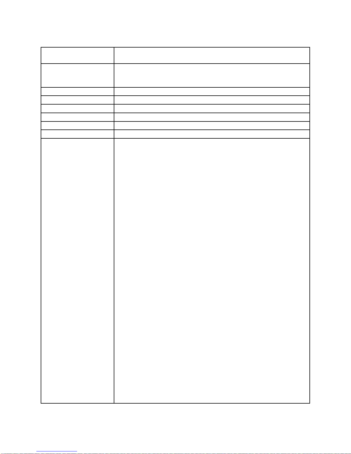
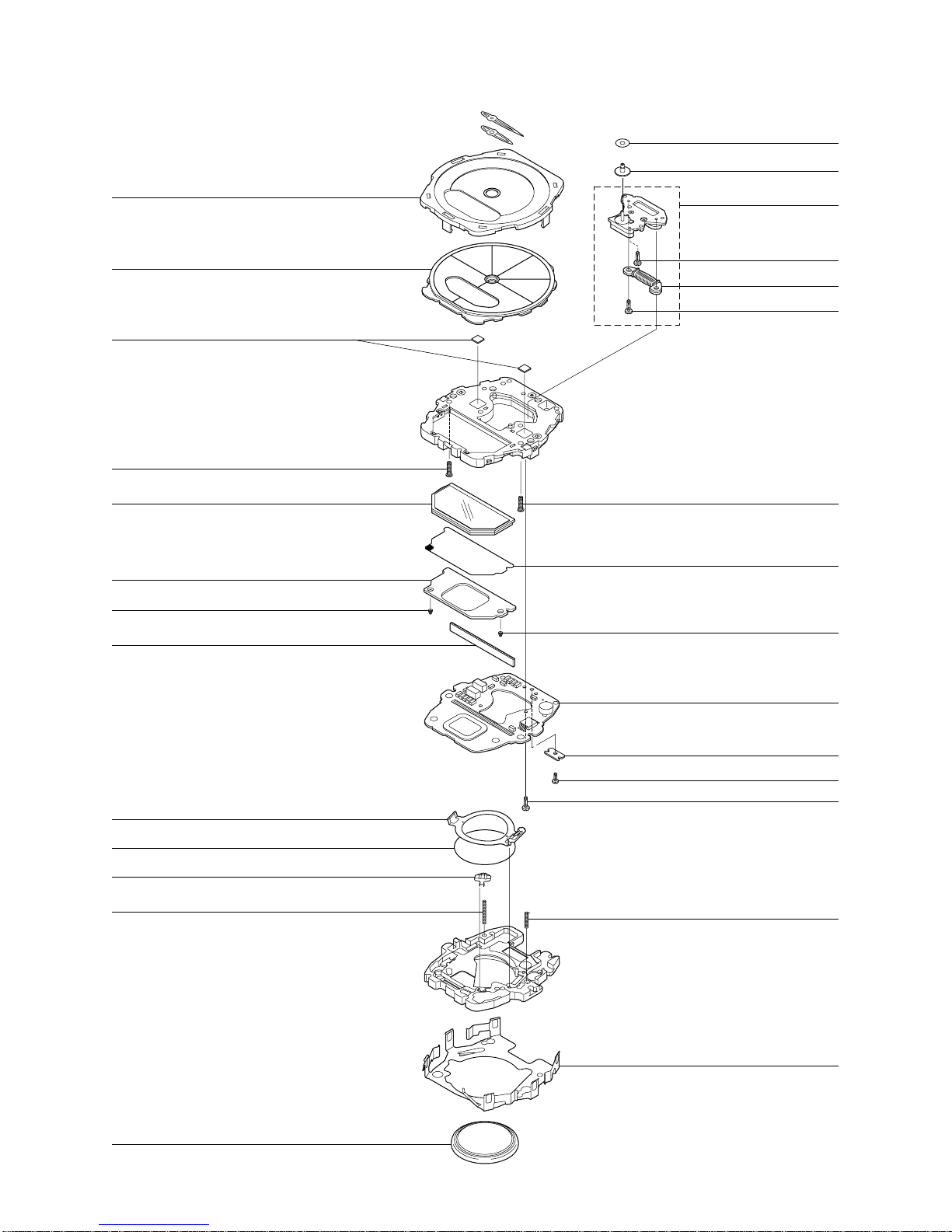
Item Code No. Parts Name Specification Applicable Q R
1009 6137 MODULE/WITH MOVEMENT QW-2741YCSA-01 WVA-310DQ-1A/2A 1A
11009 4073 LCD C2740-01 QW-2741YCSA-01 1A
21006 5665 EL YEL-2368-A-01 QW-2741YCSA-01 1A
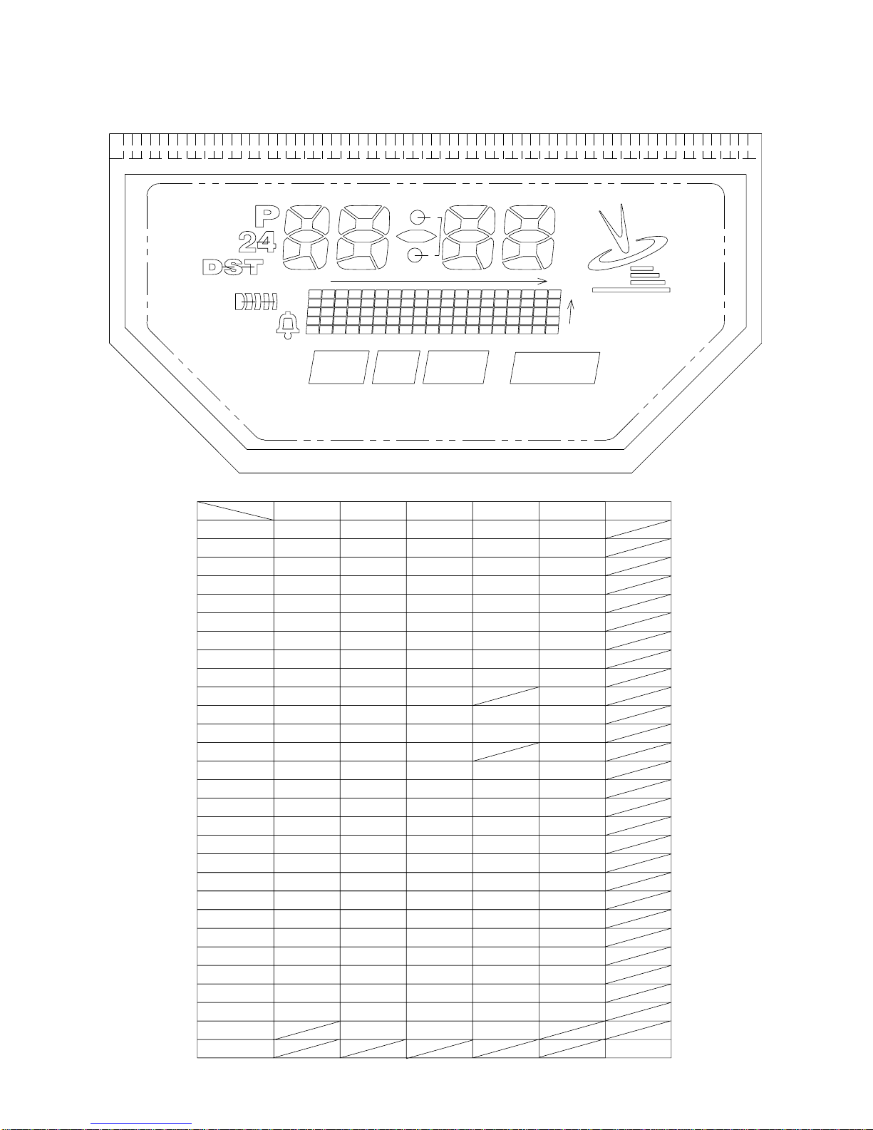
37640 6705 PCB ASS'Y Q255946*1TK QW-2741YCSA-01 1 A
41001 0950 CAPACITOR/TRIMMER CTZ2E-30C-W2-P QW-2741YCSA-01 1 B
57110 6323 OSCILLATOR/CRYSTAL DT-26S11 QW-2741YCSA-01 1 B
67640 5041 ANALOG BLOCK QW-2368MV-82TK QW-2741YCSA-01 1 A
6-1 1006 2535 COIL ASS'Y Q369124*1 QW-2741YCSA-01 1 B
6-2 7227 0273 SCREW/1300-1 Q436969A-1 QW-2741YCSA-01 2 B
71006 5657 BATTERY/STORAGE CTL1616 QW-2741YCSA-01 1 B
81001 6598 CONTACT/BATTERY(-) Q366836-1 QW-2741YCSA-01 1 C
97211 9631 CUSHION/506 Q49364-1 QW-2741YCSA-01 2 C
10 7231 1777 HOLDER 1381 Q456843-1 QW-2741YCSA-01 1 C
11 1006 5660 HOLDER 2368 Q255111A-1 QW-2741YCSA-01 1 C
12 1008 3194 HOLDER/BATTERY Q255199C-2 QW-2741YCSA-01 1 C
13 1006 5662 INTERCONNECTOR Q468267-1 QW-2741YCSA-01 1 C
14 1006 5664 LABEL 2368 Q468543A-1 QW-2741YCSA-01 1 C
15 7227 0252 SCREW Q431332-1 QW-2741YCSA-01 1 B
16 7227 0415 SCREW/TAPPING Q450646B-1 QW-2741YCSA-01 1 B
17 7640 5483 SOLAR ASS'Y Q370513*1TK QW-2741YCSA-01 1 C
18 1006 5661 SPACER Q369365-1 QW-2741YCSA-01 1 C
19 1001 4294 SPRING/COIL Q466513A-1 QW-2741YCSA-01 2 B
20 1003 0983 SPRING/COIL 2362-1 Q467328A-1 QW-2741YCSA-01 2 B
21 1006 5663 SPRING/COIL 2368 Q468519-1 QW-2741YCSA-01 1 B
22 7201 9599 SPRING/COIL 967-1 Q430081-1 QW-2741YCSA-01 1 B
23 1006 5659 SUPPORTER/PCB ASS'Y Q152109B-1 QW-2741YCSA-01 1 C
24 7229 0789 TAPE/ADHESIVE Q462101-1 QW-2741YCSA-01 1 C
25 7209 9263 TAPE/ADHESIVE 658-B Q428127-1 QW-2741YCSA-01 2 C
26 7224 0652 WASHER Q421691-1 QW-2741YCSA-01 1 C
27 1005 4633 WHEEL/HOUR Q350681D-2 QW-2741YCSA-01 1 C
For the
p
rices and minimum order/su
pp
l
y
q
uantities of the above
p
arts, refer to the Parts Price List P.P.L.-593.
Notes: Q - Used quantity
R - Rank — 6 —

—7 —
5. PRECAUTIONS FOR REPAIR: MODULE QW-2741
5-1. AC (ALL CLEAR) AND REMOVING OF MODULE
1. Perform AC (ALL CLEAR) when inserting a new battery, or else the memories and/ or counters may give
erratic displays.
Touch the AC contact and the main plate with the metallic tweezers.
The contact should be made for about two seconds.
2. On removing of the module from the case, please insert the precision screw driver between the module
and the case pointed by arrows.
5-2. ACCURACY CHECKING
Check the accuracy of the module with the quartz timer after switching the module to “ACCURACY
CHECKING MODE”.
The operations are shown below:
A) SWITCHING TO “ACCURACY CHECKING MODE”
While pressing the D button, press Aand Cbuttons at the normal timekeeping mode.
Then all the segments are displayed and the LCD drive signals are changed to the static drive signal
of “32 Hz”so that you can check the accuracy with the quartz timer.
B) CANCELLATION OF THE “ACCURACY CHECKING MODE”
Press any button.
Then the display is returned to its original state.
NOTE: The “ACCURACY CHECKING MODE” will
automatically return to the regular mode
in 1 ~ 2 hour(s) without any operation. QW-2741
A
C
B
D

— 8 —
Yes
No
Yes
No
Yes
No
Yes
No
START
Check whether the Home City
code is selected correctly.
Perform MANUAL time
calibration signal reception
OK
Perform AUTO time
calibration signal reception
Replace the PCB ass'y
Signal
reception OK?
Signal
reception OK?
Signal
reception OK?
Replace the Case center
ass'y with antenna
Signal
reception OK?
OK
OK
OK
There is a possibility of the bad location for reception.
See "Time calibration Signal Reception Precautions."
6. TROUBLESHOOTING FOR TIME RECEPTION: MODULE QW-2741
This is a flow chart about signal reception.

CASIO TECHNO CO.,LTD.
Overseas Service Division
6-2, Hon-machi 1-Chome
Shibuya-ku, Tokyo 151-8543, Japan
This manual suits for next models
2
Table of contents
Other Casio Watch manuals

Casio
Casio 1856 Configuration guide

Casio
Casio WSD-F30 User manual

Casio
Casio 5087 User manual

Casio
Casio BG-153 Troubleshooting guide

Casio
Casio 1995 User manual

Casio
Casio GW-1200BCJ Troubleshooting guide

Casio
Casio 3175 User manual

Casio
Casio 5230 User guide

Casio
Casio QW-3468 User manual

Casio
Casio Baby-G BG169R-2 User manual