manuals.online logo
Brands
  1. Home
  2. •
  3. Brands
  4. •
  5. CDS Wireless
  6. •
  7. Modem
  8. •
  9. CDS Wireless VN310 User manual

CDS Wireless VN310 User manual

VN310 RF Modem
User Manual
1
Proprietary & Confidential
1. Purpose and audience ............................................................................................................. 2
2. Pin-out and interface summary.............................................................................................. 2
3. Serial and SPI interfacing with VN310 .................................................................................. 4
4. VN310 Power Supply Considerations.................................................................................... 6
4.1. Key Specifications.................................................................................................................. 6
4.2. Electrical Characteristics ...................................................................................................... 6
4.3. External Anetnna Specifications and Installation Requirements.................................. 7
5. VN310 Mechanical Drawings ................................................................................................. 8
6. Regulatory Labeling and Notices.........................................................................................11
Control Data Systems
Version 1.0
Created: February 6th, 2017
2
Proprietary & Confidential
The purpose of this document is to define the VN310 radio’s connectivity options. It also
aims to provide the necessary data to achieve hardware integration of the VN310 with
a customer’s external application processor.
An external processing entity can communicate with the VN310 using either a UART
interface (utilizing UART2) or an SPI interface. The UART1 port is dedicated to serial
firmware download.
By definition the VN310 is essentially a small radio module, approximately 1.1”W x 1.4”L,
that is pre-loaded with the ISA100.11a communications stack. The small form factor
enables the radio to be used in a variety of applications. The VN310-I and the VN310-H
are identical from a hardware perspective and differ only by the pre-loaded factory
firmware.
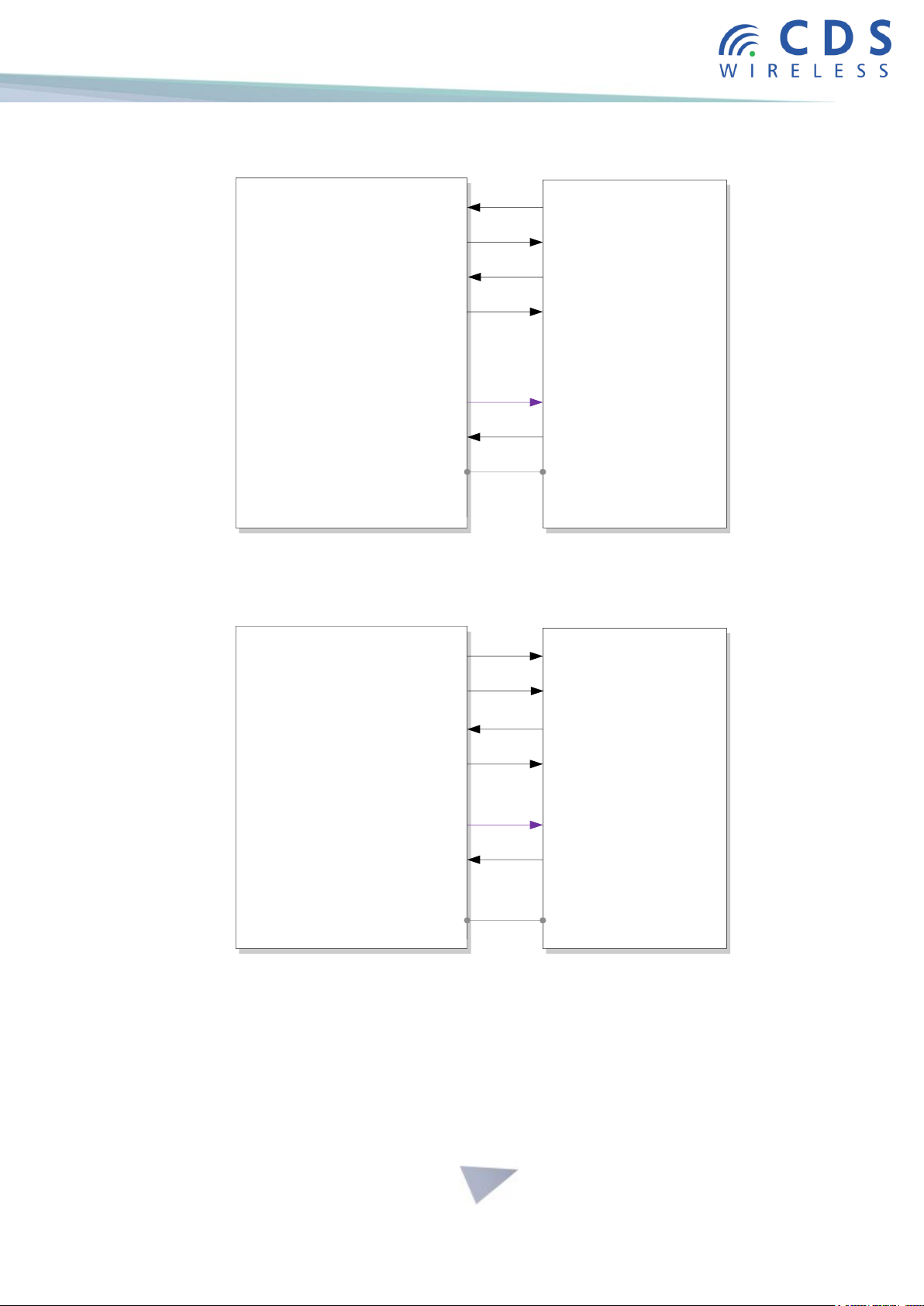
Refer to the block diagram in Figure 1 for the following section.
The VN310 radio module uses the Freescale MC13224 SoC.
The transmit path utilizes a PA (power amplifier) to increase the power output of the
VN310 module to a maximum output power at the antenna connector of +17 dBm, with
a nominal operating power level of +10 dBm. The transmit power variation vs.
temperature is no greater than +/- 3 dB over the industrial temperature range of -40
deg. C to +85 deg. C. A Digital-to-Analog converter (DAC) is used to vary the bias voltage
on the power amplifier to adjust its power and also to maintain the optimum output
power vs. current consumption. Power tuneability is accomplished by varying the PA
bias via the DAC.
The advantages of a radio module with adjustable power output are the following:
1. Ability to increase power output to +17 dBm in applications where battery
consumption is not critical or applicable.
2. Enables the unit to be configured for different regulatory certification needs, especially
locations that require reduced power, such as Europe, Japan, and China.
3. Provides greater power level consistency, for systems where symmetrical links are
more critical.
1
Proprietary & Confidential
The design of the RF section of the unit uses additional transmit components:
1. Dual LPFs to reduce harmonic output and spurious output for regulatory compliance,
such as FCC, R&TTE, and Japanese certifications.
2. Balun to match the differential output of the radio SoC to the single ended transmit
circuits.
3. Tx / Rx switch to select the transmit / receive RF path.
4. An antenna matching circuit, to ensure a 50 ohm driving source impedance into the
antenna connector. The matching will maximize power output and minimize return loss.
As shown in the block diagram, the receive path utilizes the same Tx / Rx switch and
antenna matching network. The receive path is passive without any additional
amplification.
The Freescale SoC is clocked at 24 MHz using a 20 ppm crystal to maintain frequency
stability. A 32.768 kHz real-time clock IC is utilized to maintain SoC clocking operation
during low power / standby modes. An additional external flash memory IC (serial) with
a 512 KB capacity is utilized for additional data storage. To improve reliability, a separate
hardware watchdog timer is used to reset the radio if the GPIO stops communicating
with the watchdog for more than 10 seconds. Note, this time can be adjusted to
optimize performance.
MC13224
SoC
LPF
Power
Amplifier
RF
Switch
24 MHz
Crystal
512KB
Flash memory
BALUN
Network
MMCX
32768Hz RTC
1.8v
Regulator RX
TX
MATCHING
NETWORK
VIN_3V
POWER CONTROL
Digital
Attenuator
LPF
VCC
DAC
Figure 1. VN310 Functional Block Diagram
2
Proprietary & Confidential
Figure 2 presents the physical location of the pins on the VN310, and Table 1 presents
the VN310 pin descriptions.
Note: For minimum battery consumption, all unused GPIOs should be left unconnected.
UART2_RTS
UART2_CTS
UART2_RX
UART2_TX
UART2_RTS
GND
UART1_CTS
UART1_RX
UART1_TX
I2C_SDA
I2C_SCL
TMR1
TMR0
GND
SPI_SCK
SPI_MOSI
SPI_MISO
SPI_SS
KBI_0
RTC_FOUT
KBI_6
KBI_5
GND
ADC2_VREFH
ADC2_VREFL
ADC1_VREFH
ADC1_VREFL
GPIO_1
GPIO_2
GPIO_3
GND
GPIO_7
GPIO_8
GPIO_9
GPIO_10
GPIO_11
GPIO_12
RTC_INT_B
KBI_1
KBI_2
KBI_3
KBI_4
GND
ADC3
ADC2
ADC1
ADC0
V_IN
GND
RESET_B
JTAG_RTCK
TDO
TDI
TCK
TMS
VN310
PINOUT
Figure 2. VN310 Pinout
Table 1. VN310 Pin Definitions
No.
Name
Description
Type
Dir
Comments
1
UART2-
CTS
UART2 Clear to Send
DIG
I
Standard UART communication with flow
control. Connect this to UART-RTS of
application processor.
2
UART2-
RTS
UART2 Request to Send
DIG
O
Standard UART communication with flow
control. Connect this to UART-CTS of
application processor.
3
UART2-
RXD
UART2 Receive Data
DIG
I
Standard UART communication with flow
control. Connect this to UART-TXD of
application processor.
4
UART2-
TXD
UART2 Transmit Data
DIG
O
Standard UART communication with flow
control. Connect this UART-RXD of
application processor.
5
UART1-
RTS
UART1 Request to Send
DIG
I
Not Used
6
GND
Ground
N/A
N/A
3
Proprietary & Confidential
No.
Name
Description
Type
Dir
Comments
7
UART1-
CTS
UART1 Clear to Send
DIG
O
Not Used
8
UART1-
RXD
UART1 Receive Data
DIG
I
Standard UART communication. Used for
upgrading the firmware of the VN310.
TTL<-> RS232 level shifters should be
employed when connecting to RS232
port.
9
UART1-
TXD
UART1 Transmit Data
DIG
O
Standard UART communication. Used for
upgrading the firmware of the VN220.
TTL<-> RS232 level shifters should be
employed when connecting to RS232
port.
10
I2C-SDA
I2C bus DATA
DIG
I/O
Not Used
11
I2C-SCL
I2C bus CLOCK
DIG
I/O
Not Used
12
TMR1
Timer 1 I/O
DIG
O
READY signal used to wake up the
application processor.
13
TMR0
Timer 0 I/O
DIG
I/O
Not Used
14
GND
Ground
N/A
N/A
15
SPI-SCK
SPI Clock
DIG
O
Standard SPI Communication
16
SPI-MOSI
SPI Data Out
DIG
O
Standard SPI Communication
17
SPI-MISO
SPI Data In
DIG
I
Standard SPI Communication
18
SPI-SS
SPI Slave Select
DIG
O
Standard SPI Communication
19
KBI0
RTC clock out enable /
Keyboard interface pin 0
DIG
O
Not Used
20
RTC-
FOUT
32768Hz RTC clock out
DIG
O
Not Used
21
KBI6
Keyboard interface pin 6
DIG
I
Used for Wakeup & Status (Provisioning)
button. Holding this pin low for 10
seconds causes the radio to return to the
factory defaults state and scan for a
provisioning device.
22
KBI5
Keyboard interface pin 5
DIG
I/O
Not Used
23
GND
Ground
N/A
N/A
24
ADC2-
VREFH
ADC2 reference, high pin
Analo
g
I
Set ADC2-VREFH to Low and ADC2-
VREFL to High and power the VN220 for
a few seconds to erase the flash. After
erasing the flash, set the ADC2-VREFH to
High and ADC2-VREFL to Low.
WARNING: this operation will erase the
Bootloader and all manufacturing and
non-volatile data!
25
ADC2-
VREFL
ADC2 reference, low pin
Analo
g
I
See the comments for ADC2-VREFH.
26
ADC1-
VREFH
ADC1 reference, high pin
Analo
g
I
Not Used
27
ADC1-
VREFL
ADC1 reference, low pin
Analo
g
I
Not Used
28
GPIO1
GPIO
DIG
O
Used for output gain control.
29
GPIO2
GPIO
DIG
O
Used for output gain control.
30
GPIO3
GPIO
DIG
O
Used for output gain control.
31
GND
Ground
N/A
N/A
32
GPIO7
GPIO
DIG
I/O
Not Used
33
GPIO8
GPIO
DIG
I/O
Not Used
4
Proprietary & Confidential
No.
Name
Description
Type
Dir
Comments
34
GPIO9
GPIO
DIG
I/O
Not Used
35
GPIO10
GPIO
DIG
I/O
Not Used
36
GPIO11
GPIO
DIG
I/O
Not Used
37
GPIO12
GPIO
DIG
I/O
Not Used
38
RTC-INT-B
RTC wake-up interrupt /
Keyboard interface pin 7
DIG
O
Not Used
39
KBI1
Keyboard interface pin 1
DIG
I
Used as boot switch in order to boot
different firmware images based on the
position of the switch (future
functionality). At present, this pin should
be held HIGH.
40
KBI2
Keyboard interface pin 2
DIG
I/O
Not Used
41
KBI3
Keyboard interface pin 3
DIG
I/O
Not Used
42
KBI4
Keyboard interface pin 4
DIG
I
WKU signal. Used by the application
processor to wake up the VN210
processor.
43
GND
Ground
N/A
N/A
44
ADC3
ADC pin 3
Analo
g
I
Not Used
45
ADC2
ADC pin 2
Analo
g
I
Not Used
46
ADC1
ADC pin 1
Analo
g
I
Not Used
47
ADC0
ADC pin 0
Analo
g
I
Reserved for future functionality. At
present this pin should be held HIGH.
48
Vin
Supply Voltage
N/A
I
See Note.
49
GND
Ground
N/A
N/A
50
RESET
RESET pin
DIG
I
Reset pin of the VN310. LOW to reset
and HIGH to run.
51
JTAG-
RTCK
JTAG Return Clock
DIG
O
Standard JTAG interface.
52
JTAG-
TDO
JTAG Test Data Output
DIG
O
Standard JTAG interface
53
JTAG-TDI
JTAG Test Data Input
DIG
I
Standard JTAG interface
54
JTAG-TCK
JTAG Test Data Input
DIG
I
Standard JTAG interface
55
JTAG-
TMS
JTAG Test Mode Select
DIG
I
Standard JTAG interface
Note: In the default configuration, the radio is powered from the LDO U13 (PN:
MCP1802T-3002I-OT). R29 will be depopulated. Contact CDS engineering for more
information.
5
Proprietary & Confidential
The following figures indicate the correct UART and SPI pin connectivity between the
VN310 and an external application processor.
VN310
1(ExtRTS) EXTRTS
2(ExtCTS) EXTCTS
3
(RX) UART2-RXD
4
(TX) UART2-TXD
GND
(WKU) KBI4 42
(RDY) TMR1 12
DAQ/Application
Processor
UART-RTS
UART-CTS
TX
RX
WKU_RADIO
RDY_RADIO
GND
Figure 3. Interfacing with the VN310 using UART Based Communication
VN310
15(CLK) SPI-SCK
16
(MOSI) SPI-MOSI
17
(MISO) SPI-MISO
18
(SS) SPI-SS
GND
(WKU) KBI4 42
(RDY) TMR1 12
DAQ/Application
Processor
WKU_RADIO
RDY_RADIO
GND
SCLK
MOSI
MISO
SS
Figure 4. Interfacing with the VN310 using SPI Based Communication
Connect the RDY pin only if the full wakeup communication mode is desired.
6
Proprietary & Confidential
Table 2. Key Specifications
Parameter
Min
Typ
Max
Units
Comment
Supply Voltage (3V regulated
supply)
2.94
3.0
3.06
V
Voltage on any digital I/O
-0.3
Vcc
Vcc + .02
V
V
RF Output Level
0
+10
+17
dBm
Output power at
antenna connector
Storage Temp Range (Max)
-40
+85
◦C
Operating Temp Range
(Max)
-40
+85
◦C
Table 3. Electrical Characteristics
Parameter
Min
Typ
Max
Units
Comments
Voltage on analog pins
0
3.0
Vcc
V
Voltage supply noise
200
mVpp
50Hz –15MHz
Peak current
124
mA
TX mode, maximum
output power
Operating relative humidity
10
90
%RH
Non condensing
Transmit current
67
124
mA
mA
At 10 dBm
At 17 dBm
Receive current 1)
21
27
mA
Hibernate current 2)
15
µA
Output High-level Voltage
(IOH = 5 mA) (All digital
outputs)
80%
Vcc
Vcc
V
Output Low Voltage (IOL = -5
mA) (All digital outputs)
0
20% Vcc
V
Input Low Voltage (All digital
inputs)
0
30% Vcc
V
7
Proprietary & Confidential
Input High-level Voltage (all
digital inputs)
70%
Vcc
Vcc
V
Input hysteresis (all digital
inputs)
0.06
Vcc
V
Notes:
1) All RAM active, Reference oscillator on (24 MHz) at 1.2 VDC, Radio RX on
(receiving data), Reference clock available to all peripherals, ADC1 available
but inactive, CPU on at 2 MHz (DCD).
2) External 32 kHz crystal oscillator on, CPU off (stop mode), wake-up from RTI
timer or external request, Radio off, ADCs not available.
For additional information please consult the VersaNode 310
datasheet.
Antenna Specification
8
Proprietary & Confidential
Antenna Installation requirements-The antenna(s) used for this transmitter must be installed to
provide a separation distance of at least 20 cm from all persons and must not be co-located or operating
in conjunction with any other antenna or transmitter.
Figure 5. Shield
9
Proprietary & Confidential
VN310 MECHANICAL
DIMENSIONS
Figure 6. Outline Drawing
10
Proprietary & Confidential
Figure 7. Dimension Drawing
11
Proprietary & Confidential
Figure 8. Recommended Footprint
FCC Notice-This device complies with Part 15 of the FCC rules. Operation is subject
to the following two conditions: (1) this device may not cause harmful interference, and
(2) this device must accept any interference received, including interference that may
cause undesired operation.
This equipment has been tested and found to comply with the limits for a Class B digital
device, pursuant to part 15 of the FCC Rules. These limits are designed to provide
reasonable protection against harmful interference in a residential installation. This
equipment generates uses and can radiate radio frequency energy and, if not installed
and used in accordance with the instructions, may cause harmful interference to radio
12
Proprietary & Confidential
communications. However, there is no guarantee that interference will not occur in a
particular installation. If this equipment does cause harmful interference to radio or
television reception, which can be determined by turning the equipment off and on, the
user is encouraged to try to correct the interference by one or more of the following
measures:
Reorient or relocate the receiving antenna.
Increase the separation between the equipment and receiver.
Connect the equipment into an outlet on a circuit different from that to which the
receiver is connected.
Consult the dealer or an experienced radio/TV technician for help.
Warning: Modifications to this equipment not expressly approved by manufacturer will
void the user's authority to operate the equipment!
The VN310 RF Module has been certified per FCC Part 15 rules for integration into
products without further testing or certification. To fulfill the FCC certification
requirements the OEM of the VN310 RF Module must ensure that the information
provided on the VN310 RF Module label is placed on the outside of the final product.
The VN310 RF Module is labeled with its own FCC ID Number. If the FCC ID is not visible
when the module is installed inside another device, then the outside of the device into
which the module is installed must also display a label referring to the enclosed module.
This exterior label can use wording such as the following:
“Contains Transmitter Module FCC ID: 2AKZ5-CDSVN310” or
“Contains FCC ID: 2AKZ5-CDSVN310”
IC RSS-210 Notice- Operation is subject to the following two conditions: (1) this device
may not cause interference, and (2) this device must accept any interference, including
interference that may cause undesired operation of the device.

Popular Modem manuals by other brands

Draytek Vigor2832 Series quick start guide

Draytek

Draytek Vigor2832 Series quick start guide

Teledyne Quantum Series Installation and operating handbook

Teledyne

Teledyne Quantum Series Installation and operating handbook

NetComm NCT-1000 Technical specifications

NetComm

NetComm NCT-1000 Technical specifications

Telecom Let's Go Getting started guide

Telecom

Telecom Let's Go Getting started guide

Chonghan CH-M3 user manual

Chonghan

Chonghan CH-M3 user manual

SIRETTA ZEST SERIES quick start guide

SIRETTA

SIRETTA ZEST SERIES quick start guide

MaxStream 9 XCite-PKG-U XC09-009PK-U Series product manual

MaxStream

MaxStream 9 XCite-PKG-U XC09-009PK-U Series product manual

Motorola SURFboard SB4101 install guide

Motorola

Motorola SURFboard SB4101 install guide

Black Box ME375A quick start guide

Black Box

Black Box ME375A quick start guide

Multitech SocketModem Series Device guide

Multitech

Multitech SocketModem Series Device guide

Black Box ME800A Plus instruction manual

Black Box

Black Box ME800A Plus instruction manual

red lion MobilityPro BT-5600 Series quick start guide

red lion

red lion MobilityPro BT-5600 Series quick start guide

Multitech MultiModem II MT5600BA-V.92 user guide

Multitech

Multitech MultiModem II MT5600BA-V.92 user guide

Multitech MultiModem MT2834ZDX Series Quick reference guide

Multitech

Multitech MultiModem MT2834ZDX Series Quick reference guide

Multitech MT5634HD16 user guide

Multitech

Multitech MT5634HD16 user guide

Black Box SHM-768K Series manual

Black Box

Black Box SHM-768K Series manual

EQ3 USB programming stick for radio energy-saving... operating manual

EQ3

EQ3 USB programming stick for radio energy-saving... operating manual

IP Wireless 1C user guide

IP Wireless

IP Wireless 1C user guide

manuals.online logo
manuals.online logoBrands
  • About & Mission
  • Contact us
  • Privacy Policy
  • Terms and Conditions

Copyright 2025 Manuals.Online. All Rights Reserved.