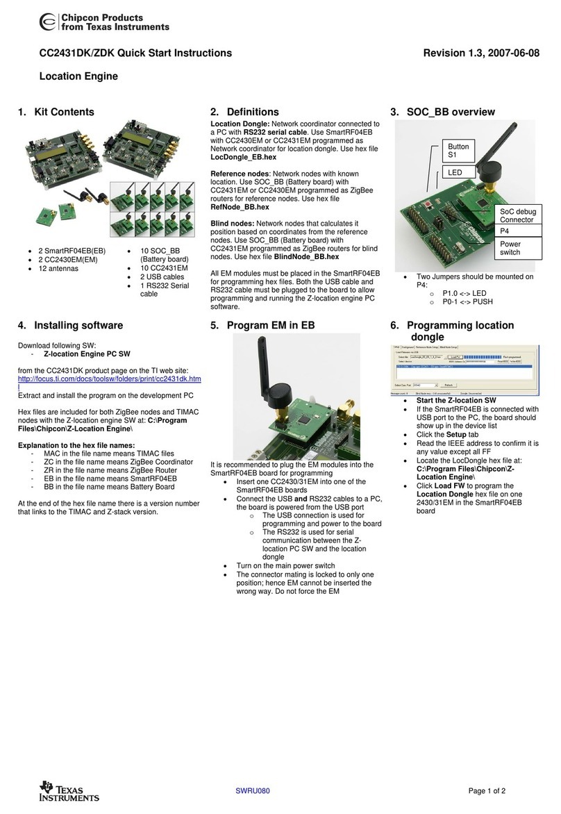
Chipcon SmartRF CC2420DBK User manual

User Manual
Rev. 1.3
SmartRF
®
CC2420DBK Demonstration Board Kit
Chipcon AS, Gaustadalléen 21, NO-0349 Oslo, Norway. Tel: +47 22 95 85 45, fax: +47 22 95 85 46.
E-mail: [email protected]

Chipcon AS SmartRF
®
CC2420DBK Demonstration Board Kit User Manual (rev. 1.3) 2004-11-03 Page 2/ 52
Table of contents
INTRODUCTION ......................................................................................................................3
PCB.......................................................................................................................................4
A
NTENNA
................................................................................................................................5
P
OWER SUPPLY SECTION
.........................................................................................................7
RS-232
INTERFACE
.................................................................................................................8
M
ICROCONTROLLER AND USER INTERFACE
...............................................................................8
E
XTERNAL
RAM......................................................................................................................8
F
LASH
M
EMORY
R
EQUIREMENTS
.............................................................................................8
CC2420DB L
OW
P
OWER
M
ODE SUPPORT
...............................................................................8
J
UMPER SETTINGS FOR DEMONSTRATION BOARD CONTROL
........................................................9
CC2420DB C
URRENT
M
EASUREMENT AND
C
ONSUMPTION
....................................................11
PCB
LAYOUT
........................................................................................................................16
B
ILL OF
M
ATERIALS
...............................................................................................................25
USING THE CC2420DB DEMONSTRATION BOARD .........................................................30
CC2420 S
OFTWARE
D
OWNLOAD AND
E
VALUATION
U
SING
AVR S
TUDIO
4..............................30
P
REPROGRAMMED
64-
BIT
IEEE A
DDRESS
.............................................................................30
P
REPROGRAMMED
F
USES
......................................................................................................31
P
REPROGRAMMED
L
OCK
B
ITS
................................................................................................33
JTAG ICE
OR
JTAG ICE
MK
II ..............................................................................................33
S
AVING THE
IEEE A
DDRESS OF THE
CC2420DB ...................................................................34
R
ESTORING THE
IEEE A
DDRESS OF THE
CC2420DB.............................................................36
A N
EW
D
EBUGGING
P
ROJECT
W
ITH
CC2420DB....................................................................38
B
OOTLOADER
........................................................................................................................43
I
NTRODUCTION TO
E
XAMPLES
P
ROVIDED WITH
CC2420DB ....................................................45
LIBRARIES AND EXAMPLES...............................................................................................45
H
ARDWARE
D
EFINITION
F
ILES
................................................................................................45
H
ARDWARE
A
BSTRACTION
L
IBRARY
(HAL) .............................................................................45
B
ASIC
RF L
IBRARY
................................................................................................................46
S
OFTWARE
E
XAMPLE
P
ROGRAMMED ON
CC2420DB .............................................................46
D
ATA PACKET DESCRIPTION
...................................................................................................47
D
ATA TRANSMISSION PROTOCOL
............................................................................................48
TROUBLESHOOTING ...........................................................................................................49
I
T DOES NOT WORK
................................................................................................................49
I
CANNOT PROGRAM THE
AVR
USING THE SERIAL PORT
...........................................................49
B
OOT RESET VECTOR ENABLE
................................................................................................49
B
OOTLOADER
........................................................................................................................49
REFERENCES .......................................................................................................................50
ADDRESS INFORMATION....................................................................................................51

Chipcon AS SmartRF
®
CC2420DBK Demonstration Board Kit User Manual (rev. 1.3) 2004-11-03 Page 3/ 52
Introduction
The CC2420 is a single-chip IEEE 802.15.4 compliant and ZigBee™ ready RF transceiver. It
provides a highly integrated, flexible low-cost solution for applications using the world wide
unlicensed 2.4 GHz frequency band. The CC2420DBK demonstration board kit is a
complement to the development kit (DK) as the hardware is representative of an actual
application, and it is well suited as a prototyping platform for application code.
The CC2420DBK Demonstration Board Kit includes two CC2420DB Demonstration Boards.
These boards contain a CC2420 with necessary support components, an Atmel Atmega128L
AVR microcontroller, 32 kBytes external RAM, a PCB antenna, as well as a joystick, buttons
and LED's that can be used to implement a visual user application interface. The
demonstration board is also furnished with connectors where all of the internal signals on the
PCB are available.
This User Manual describes how to use the CC2420DBK Demonstration Board Kit. Atmel’s
AVR Studio and associated software is used to program and debug software. Please see the
reference section of this document for links to Atmel’s documentation on how to use their
tools.
Your CC2420DBK Demonstration Board Kit should contain the following items:
Kit contents
Item Number of articles
Demonstration Board (CC2420DB) 2
Quick Start instructions 1
CC2420DB Important Notice (From revision 1.5 and newer) 1
CC2420 sample kit 1
RS-232 cable 2
Important:
Contact your local telecommunication authorities before transmitting an RF signal to ensure
that there are no local restrictions on the use of the 2.400 –2483.5 ISM band. The CC2420
operates in the 2.4 GHz frequency band. Although this frequency band is usually described
as “world-wide”, some countries do not allow unlicensed operation in this band.

PCB
PCB depicts an overview of the CC2420DB with description of the various components
embedded on the PCB.
3.3V voltage
regulator
Optional 9V
or 4x 1.5 AA
battery
AVR ISP
connector
Chipcon AS SmartRF
®
CC2420DBK Demonstration Board Kit User Manual (rev. 1.3) 2004-11-03 Page 4/ 52
Figure 1: CC2420DB overview
RF Section
The CC2420DB RF section includes all the necessary components for correct operation. The
CC2420 is connected to a 16 MHz crystal. A small 2.4 GHz PCB antenna is also included. RF
test and measurement equipment can be connected to the SMA on the PCB, by swapping
Temp. sensor
External RAM
1 x 32 kB
JTAG
connecto
r
MCU
section
CC2420 RF
section
PCB
antenna
RS-232
port
POT Joystick
4-10 V
DC-jack
LED’sButtons

capacitor placement of C63 and C62. See schematics for details. The RF layout is identical to
the CC2420EM, which is part of the CC2420DK Development Kit.
Antenna
The PCB antenna is a so-called Inverted-F type. The Inverted-F antenna is a wire monopole
where the top section is folded down to be parallel with the ground plane. By folding the
antenna down you will reduce the height and maintain a resonant wire length. A capacitance
will be introduced to the input impedance of the antenna due to the parallel section. However,
as a rule of thumb design guide, the length + height (L+H) will be approximately equal to a
quarter wavelength (λ/4). A reduction of the antenna height (H) will in general decrease the
antenna bandwidth. Please see Figure 2 for the antenna dimensions.
Figure 2: Antenna dimensions
The height of the antenna is defined as the distance from the ground plane to the parallel
section, and the length is from the end of the antenna parallel section to the feed point.
Length: L = (26.19 mm – 9.19 mm + 1.22 mm x ½) = 17.61 mm
Height: H = (6.17 mm + 0.97 mm - 1.19 mm x ½) = 6.55 mm
Quarter wavelength: λ/4 = (L + H) = 17.61 mm + 6.55 mm = 24.16 mm
The physical size of the antenna is decreased somewhat compared to the theoretical length,
(λ= c/4*f = 3x10⁸/ 4x2.45x109) = 30.61 mm
The radiated pattern for the PCB antenna was measured with the horizontal polarization
direction for the CC2420DB by measuring with vertical and horizontal mounting of the
demonstration board.
Important:
Chipcon AS SmartRF
®
CC2420DBK Demonstration Board Kit User Manual (rev. 1.3) 2004-11-03 Page 5/ 52

In practical range testing outdoors with line-of-sight (LOS) and use of the wireless dimmer
application example, the following range has been verified at Chipcon Norway with optimal
SmartRF Studio settings for the respective data rates:
1. Data rate settings 250 kbps, range measured: 170 meters
Please note that these range tests were performed with a simple packet protocol, no link
margin, no robust protocol, close to the sensitivity limit of CC2420, and no retransmission.
CC2420DB
0 degr.
Top view
Antenna
Figure 3: Radiated pattern horizontal mounting
Figure 3 depicts the antenna pattern while the CC2420DB is mounted horizontally with the
antennas parallel section aligned to the 0 degree direction.
Chipcon AS SmartRF
®
CC2420DBK Demonstration Board Kit User Manual (rev. 1.3) 2004-11-03 Page 6/ 52

Antenna
CC2420DB
0 degr.
Top view
Figure 4: Radiated antenna pattern vertical mounting
Figure 4 depicts the antenna pattern while the CC2420DB is mounted vertically with the
antennas parallel section aligned to the 0 degree direction.
The peak antenna gain is –5 dBi, the corresponding peak field strength is 90dBuV/m.
Power supply section
The power supply section contains two voltage regulators: a 3.3 V regulator for use by the
microcontroller and the I/O pins of the CC2420. The internal regulator of CC2420 is used to
generate the 1.8 voltage supply applied for powering of the CC2420 core.
A diode prevents permanent damage if wrong polarity is applied to the board. There are two
power connectors; a 2.5mm DC jack-type connector allows you to connect an unregulated
battery eliminator easily (the positive supply is on the center pin), and a connector for a 9V
battery on the bottoms side of the PCB. It is also possible to use 4 AA or AAA alkaline cells to
power the CC2420DB if a suitable battery pack is used.
Chipcon AS SmartRF
®
CC2420DBK Demonstration Board Kit User Manual (rev. 1.3) 2004-11-03 Page 7/ 52

Chipcon AS SmartRF
®
CC2420DBK Demonstration Board Kit User Manual (rev. 1.3) 2004-11-03 Page 8/ 52
RS-232 interface
A serial port is included on the CC2420DB. This port is used when software is programmed
into the AVR MCU using the bootloader, and is also used by several of the example
programs. The port includes support for RTS/CTS-type hardware flow control (handshaking).
Microcontroller and user interface
The microcontroller used is an AVR Atmega128L from Atmel. This controller has 128 KB of
Flash program memory, 4 KB of SRAM data memory and 4 KB of non-volatile EEPROM data
memory. The controller is interfaced to the CC2420 via its built-in SPI interface as well as
some general I/O pins.
The MCU is also connected to four LED’s, a joystick and an extra button for user interface
purposes. The different examples use these peripherals differently. An analog temperature
sensor, a potentiometer and 64K of external RAM are also included.
An ISP and a JTAG ICE connector are provided for programming the AVR without using the
serial port. In this case an Atmel AVR JTAG or ISP programmer should be connected to their
respective connectors.
All of the I/O pins are connected to footprints for 2 x 10 pin-row connectors. These connectors
are compatible with Agilent logic analyzer probes, and can be used either for testing or for
prototyping. For instance, it is possible to add a daughter board with additional circuitry using
these connectors.
External RAM
The lower 4 Kbytes of the external RAM is overlaid by the Atmega128L internal register and
RAM. CC2420DB includes this memory because it can be used for debugging purposes, to
buffer and store data if desired. The 32 kB RAM size is not a requirement nor necessary for a
low cost a Full Functional Device (FFD) or Reduced Functional Device (RFD). Please refer to
the Atmega128L data sheet for more details.
Flash Memory Requirements
The flash requirement for a FFD device with the Chipcon MAC will be approximate 20 kBytes
and 10 - 16 kBytes for a RFD. Additional flash size must be available for the application.
Important:
The memory requirement will be dependant on compiler, optimization level, hardware
platform and feature used in the stack.
CC2420DB Low Power Mode support
To apply a low power mode with CC2420DB for application development, it will be necessary
to apply an additional clock source together with the 8 MHz crystal. The Atmega128L
provides the Timer/Counter oscillator pins (TOSC1 and TOSC2), and these pins are available
on the CC2420DB connector P3. The oscillator is optimized for use with a 32.768 kHz crystal.
This clock source can be connected the following ways.
1. A crystal can be connected directly between the pins.
2. An external clock source can be applied to the TOSC1. Atmel does not recommend
this method.
The 32.768 kHz crystal will clock the timer 0 and then the overflow or compare match timer
interrupt is applied to wake up Atmega128 from power save mode.

Chipcon AS SmartRF
®
CC2420DBK Demonstration Board Kit User Manual (rev. 1.3) 2004-11-03 Page 9/ 52
Name Connector P3 Atmega12
8
TOSC1 (PG4) Pin 9 Pin 19
TOSC2 (PG3) Pin 7 Pin 18
Table 1, Low power mode signal
To demonstrate an application using the power down mode:
1. Apply 4x 1.5 AA batteries with a battery clip to the battery connector.
2. The library macros will be made available on how to set the ATmega128L into the
various power mode that can be applied to minimize the current draw on CC2420DB.
3. Apply the joystick switch as the external interrupt to wake up the ATmega128L to idle
mode and run an application.
CC2420DB temperature range
The CC2420DB can support a temperature range of -30˚C to +85˚C limited by the crystal
tolerance and the CC2420 temperature range.
Jumper settings for demonstration board control
The CC2420DB demonstration board has three default jumper settings for proper operation.
Figure 5 depicts the placement of the three jumpers J1, J2 and J3. They are mounted on
connector P9. Please see CC2420DB schematics page 1 for more details.
Jumper Purpose Comments
J1 To apply power of 3.3 volt to
the circuitry on the PCB
board
An option can be to remove
the jumper and connect an
ampere meter in series to
measure current
consumption
J2 To apply power of 3.3 volt to
the potentiometer and
temperature sensor on the
PCB board
Can be removed to
disconnect the devices if not
used, to decrease current
consumption
J3 To always have the RS-232
driver enabled, hence the
driver is forced on
This jumper can be
disconnected and instead
controlled by software if
desired
Table 2 Jumpers explanation

J2J3
J1
Figure 5 Jumpers
Jumper J1 Jumper J3
Jumper J2
Figure 6 Jumpers on CC2420DB
To enable software control of the RS-232 driver U101, the jumper J3 can be moved.
Step-By-Step procedure:
1. Move RS-232 jumper J3 from P9 to P3 between pin 3 and 4
2. It will share the same port pin PE4 as the yellow LED, so when RS-232 is on the LED
will be set.
Chipcon AS SmartRF
®
CC2420DBK Demonstration Board Kit User Manual (rev. 1.3) 2004-11-03 Page 10/ 52

CC2420DB Current Measurement and Consumption
It is fully possible to measure the actual current consumption with CC2420DB. To measure
the current jumper J1 must be removed and an ampere meter connected in series. The
current measurement is performed for the current total draw of the CC2420DB.
A
P3
12
Figure 7: Connector P3 with ampere meter attached
To help minimize the current consumption of the CC2420DB for a specific IEEE 802.15.4
devices the default jumper J3 can be moved to enable software control of the RS-232 driver.
The external RAM will always draw 2mA in any power down mode since its power supply
cannot be disabled. Hence, if the external RAM (U3) is removed the current consumption will
decrease with 2mA.
The jumper J2 is controlling the power for the potentiometer (RT1) and temperature sensor
(U2), which will also contribute to the total current consumption in any power down mode.
Chipcon AS SmartRF
®
CC2420DBK Demonstration Board Kit User Manual (rev. 1.3) 2004-11-03 Page 11/ 52

Chipcon AS SmartRF
®
CC2420DBK Demonstration Board Kit User Manual (rev. 1.3) 2004-11-03 Page 12/ 52
AVR I/O pins
AVR Pin
Number
AVR pin name Pin usage I/O connector
1 |PEN N.C. N/A
2 PE0 RXD0/(PDI) Joystick up / ISP MOSI P6 pin 4, P3 pin 6
3 PE1 (TXD0/PDO) Joystick right / ISP MISO P6 pin 1, P3 pin 8
4 PE2 (XCK0/AIN0) Joystick centre push button P3 pin 5
5 PE3 (OC3A/AIN1) Red LED P3 pin 11
6 PE4 (OC3B/INT4) Yellow LED P3 pin 4
7 PE5 (OC3C/INT5) Switch S2 P3 pin 10
8 PE6 (T3/INT6) Interrupt from joystick P3 pin 12
9 PE7 (IC3/INT7) General purpose I/O P3 pin 14
10 PB0 (SS) SPI Interface, CSn, CC2420 P4 pin 13
11 PB1 (SCK) SPI Interface, SCLK, CC2420 P6 pin 3, P4 pin 4
12 PB2 (MOSI) SPI Interface, SI, CC2420 P4 pin 8
13 PB3 (MISO) SPI Interface, SO, CC2420 P4 pin 6
14 PB4 (OC0) Orange LED P3 pin 18
15 PB5 (OC1A) VREG_EN, Enable volt
regulator on CC2420
P4 pin 10
16 PB6 (OC1B) RESETn, CC2420 P4 pin 16
17 PB7 (OC2/OC1C) Green LED P3 pin 16
18 PG3/TOSC2 External 32 kHz crystal /
General purpose I/O
P3 pin 7
19 PG4/TOSC1 External 32 kHz crystal /
General purpose I/O
P3 pin 9
20 |RESET Reset: Switch S2, ISP, JTAG P4 pin 3, P6 pin 5,
P10 pin 6
21 VCC Supply power N/A
22 GND Ground N/A
23 XTAL2 Crystal Oscillator N/A
24 XTAL1 Crystal Oscillator N/A
25 PD0 (SCL/INT0) FIFOP interrupt from CC2420 P4 pin 14
26 PD1 (SDA/INT1) FIFO interrupt from CC2420 P4 pin 12
27 PD2 (RXD1/INT2) UART 1, RS232, RXD1 P3 pin 15
28 PD3 (TXD1/INT3) UART 1, RS232, TXD1 P3 pin 19
29 PD4 (IC1) Polling SFD on CC2420 P4 pin 19
30 PD5 (XCK1) UART 1, RS232, RTS P3 pin 13
31 PD6 (T1) Polling CCA on CC2420 P4 pin 18

Chipcon AS SmartRF
®
CC2420DBK Demonstration Board Kit User Manual (rev. 1.3) 2004-11-03 Page 13/ 52
AVR I/O pins
AVR Pin
Number
AVR pin name Pin usage I/O connector
32 PD7 (T2) UART 1, RS232, CTS P3 pin 17
33 PG0 (|WR) WR_N, Write RAM N/A
34 PG1 (|RD) RD_N, Read RAM N/A
35 PC0 (A8) RAM address N/A
36 PC1 (A9) RAM address N/A
37 PC2 (A10) RAM address N/A
38 PC3 (A11) RAM address N/A
39 PC4 (A12) RAM address N/A
40 PC5 (A13) RAM address N/A
41 PC6 (A14) RAM address N/A
42 PC7 (A15) Select RAM, (upper / lower 32K) N/A
43 PG2 (ALE) Latch enable N/A
44 PA7 (AD7) RAM address + Data N/A
45 PA6 (AD6) RAM address + Data N/A
46 PA5 (AD5) RAM address + Data N/A
47 PA4 (AD4) RAM address + Data N/A
48 PA3 (AD3) RAM address + Data N/A
49 PA2 (AD2) RAM address + Data N/A
50 PA1 (AD1) RAM address + Data N/A
51 PA0 (AD0) RAM address + Data N/A
52 VCC Supply power N/A
53 GND Ground N/A
54 PF7 (ADC7/TDI) JTAG interface P10 pin 9
55 PF6 (ADC6/TDO) JTAG interface P10 pin 3
56 PF5 (ADC5/TMS) JTAG interface P10 pin 5
57 PF4 (ADC4/TCK) JTAG interface P10 pin 1
58 PF3 (ADC3) Temperature sensor (ADC) P4 pin 9
59 PF2 (ADC2) Joystick down P4 pin 7
60 PF1 (ADC1) Joystick left P4 pin 5
61 PF0 (ADC0) Potentiometer (ADC) P4 pin 11
62 AREF Reference voltage for ADC P4 pin 2
63 GND Ground N/A
64 AVCC ADC voltage ref N/A
Table 3: AVR I/O pins

Chipcon AS SmartRF
®
CC2420DBK Demonstration Board Kit User Manual (rev. 1.3) 2004-11-03 Page 14/ 52
P3 pinout
Pin
number
Signal name in
schematic
Pin usage AVR pin
1 N.C. N/A N/A
2 Unregulated supply voltage
(Insert R101 to connect)
3 FORCE_ON RS-232 on/off 05 PE3
4 PE4 Yellow LED 06 PE4
5 PE2 Joystick centre push button 04 PE2
6 PE0 ISP MOSI / Joystick up 02 PE0
7 PG3 External 32 kHz crystal /
General purpose I/O
18 PG3
8 PE1 ISP MISO / Joystick right 03 PE1
9 PG4 External 32 kHz crystal /
General purpose I/O
19 PG4
10 PE5 Push button S2 07 PE5
11 PE3 Red LED N/A
12 PE6 Joystick interrupt 08 PE6
13 RTS RS-232 handshaking 30 PD5
14 PE7 External interrupt / General
purpose I/O
09 PE7
15 RXD1 RS-232 data from PC 27 PD2
16 PB7 Green LED 17 PB7
17 CTS RS-232 handshaking 32 PD7
18 PB4 Orange LED 14 PB4
19 TXD1 RS-232 data to PC 28 PD3
20 GND Ground N/A
Table 4: P3 pinout

Chipcon AS SmartRF
®
CC2420DBK Demonstration Board Kit User Manual (rev. 1.3) 2004-11-03 Page 15/ 52
P4 pinout
Pin
number
Signal name in
schematic
Pin usage CC2420 pin AVR pin
1 N.C. N/A N/A N/A
2 AREF Voltage reference for A/D
Converter.
N/A 62
3 RESET Reset N/A 20
4 SCLK CC2420 SPI clock, AVR
ISP
32 (SCLK) 11
5 PF1 Joystick left N/A 60
6 SO CC2420 SPI out 34 (SO) 13
7 PF2 Joystick N/A 59
8 SI CC2420 SPI in 33 (SI) 12
9 PF3 Temperature sensor N/A 58
10 VREG_EN CC2420 voltage regulator
enable
41 (VREG_EN) 15
11 PF0 Potentiometer N/A 61
12 FIFO CC2420 FIFO 30 (FIFO) 26
13 CSn CC2420 SPI chip select 31 (CSn) 10
14 FIFOP CC2420 FIFOP 29 (FIFOP) 25
15 3.3V 3.3V Regulated supply N/A N/A
16 RESETn CC2420 Reset 21 (RESETn) 16
17 N.C. N/A N/A N/A
18 CCA CC2420 Clear Channel
Assessment
28 (CCA) 31
19 SFD CC2420 Start of Frame
Delimiter
27 (SFD) 29
20 GND Ground N/A N/A
Table 5: P4 pinout

PCB layout
RF circuits operating at high frequencies are normally sensitive to the physical layout of the
PCB. Chipcon has carefully optimized the layout of the CC2420DB Demonstration Board and
we therefore recommend that our customer copy, at least the RF parts and the decoupling
around the CC2420 when making their own PCB designs.
The PCB is of a 4-layer type in order to provide a well-defined ground plane as well as
adequate routing space. The laminate used is standard FR-4 board material. The PCB is
1.0mm thick, with layer 1 on the topside, layers 2 and 3 are internal layers and layer 4 is on
the bottom side. Layers 1 and 4 are used for routing, while layer 2 is a ground plane and layer
3 is used for power routing. All areas in the RF section that are not utilized for routing are
filled with copper connected to ground to provide RF shielding. The ground planes on all
layers are stitched together with closely spaced vias. Please see figure 8 for a board stack up
for the CC2420DB PCB.
Figure 8: CC2420DB Layer Build Up
Chipcon AS SmartRF
®
CC2420DBK Demonstration Board Kit User Manual (rev. 1.3) 2004-11-03 Page 16/ 52

Layer 1 Layer 2
Layer 3 Layer 4
Figure 9: CC2420DB PCB layout
Chipcon AS SmartRF
®
CC2420DBK Demonstration Board Kit User Manual (rev. 1.3) 2004-11-03 Page 17/ 52

Top Assembly Bottom Assembly
Figure 10: CC2420DB PCB layout silkscreen
Chipcon AS SmartRF
®
CC2420DBK Demonstration Board Kit User Manual (rev. 1.3) 2004-11-03 Page 18/ 52

Schematic
Figure 11: CC2420DB schematic page 1
Chipcon AS SmartRF
®
CC2420DBK Demonstration Board Kit User Manual (rev. 1.3) 2004-11-03 Page 19/ 52

Figure 12: CC2420DB schematic page 2
Chipcon AS SmartRF
®
CC2420DBK Demonstration Board Kit User Manual (rev. 1.3) 2004-11-03 Page 20/ 52
Other manuals for SmartRF CC2420DBK
1
Table of contents
Other Chipcon Microcontroller manuals
Popular Microcontroller manuals by other brands
ST
ST STM32F429I-DISCO user manual
Infineon
Infineon EVAL-M3-302FTOBO1 user guide
Microchip Technology
Microchip Technology MCP1631 Reference design
NXP Semiconductors
NXP Semiconductors AN10815 Application note

Atmel
Atmel SAM4SD32B Preliminary data sheet
NXP Semiconductors
NXP Semiconductors UM108 Series user guide
