Clevo Model 7200 User manual

1
Model 7200
Preliminary Service Manual
Mainboard 77-72000-D02
LED 77-72004-D00
D/D & Charger 77-7200C-D02
Daughter Board 77-7200I-D10
LVDS 77-720FL-D00
Specifications are subject to change without notice. July 1997
:

2
Specifications
The Notebook Computer is a state-of-the-art, high performance, portable system. It
offers a host of features specially designed to enhance performance and usability.
lCPU
üIntel P54C
üIntel P54LM
üIntel P55C with MMX technology.
lMemory
ü3.3 V power supply.
üSupports Fast Page Mode/EDO.
ü512KB secondary cache pipeline burst synchronous SRAM.
ü8MB expandable up to 128MB.
ü8/16/32/64MB 144-pin SODIMM RAM modules (option).
lSystem BIOS
ü256KB flash ROM.
üPCI2.1.
üPlug and Play 1.0a.
lDisplay
ü13.0” DSTN XGA (1024x768 pixels) LCD panel available.
ü13.3”/14.1” TFT XGA (1024x768 pixels) LCD panel.
ü4MB display memory.
üVideo Port Manager (VPM) for Zoomed Video (ZV) port.
üSimultaneous display with an external monitor.
lInput/Output
üBuilt-in trackpad (PS/2).
üDual USB ports.
üSerialport.
üParallel port.
üCRT port.
üGame port.
üS-Video port.
üPS/2 type port.
ü168-pin expansion port.
üHeadphone jack.
üMicrophone-in jack.
üLine-in jack.

3
lPC Card Sockets
üOne Type III or two Type II PC cards.
üCardBus support.
üOne ZV-capablesocket.
lMass Storage
ü2.5” (19mm high or less) or 3.0” (12.5mm high or less) hard disk drive.
ü3.5” floppy disk drive (interchangeable).
ü5.25” CD-ROM.
ü2.5” or 3.0” secondary hard disk drive. (option).
lInfrared Wireless Communication
üIrDA.
üASKIR.
üFIR.
lAu dio
üSound Blaster Pro compatible.
ü3D stereo sound effects.
üBuilt-in microphone.
ü1MB ROM wavetable.
lPower Management
üDoze mode.
üSuspend/Resume.
üDisplay idle mode.
üHard disk idle mode.
üAPM 1.2.
lRechargeable battery Pack
üNi-MHorLi-Ion available.
üBattery low warning.
üAuto-switching with AC power adapter.
üSecondary Battery Pack (option).
lAC Power Supply: Model AC-D01
lSize & Weight
ü323mm(w)x263.5mm(d)x58mm(h)
ü323mm(w)x263.5mm(d)x74mm(h) (stand protrusion included)
ü4.15kg.

4
I/O Address Map
Hex range
Device
000-00F
DMA controller-1
020-021
Interrupt controller-1
040-043
Timer 1
048 -04B
Timer 2
060 -06E
KB controller M38813 chip select
070-071
RTC and NMI mask
080-08F
DMA page register
0A0 -0A1
Interrupt controller-2
0C0 -0DF
DMA controller-2
1F0 -1F7
Fixed disk select
3F6 , 3F7
2F8 -2FF
Serial port 2
378-37A
Parallel port 1
3B4 , 3B5
CRT controller index (mono)
3D4 , 3D5
CRT controller index (color)
3BA
Feature control
3C0 -3DA
3F2 -3F7
Floppy disk controller
3F0 , 3F1
Configuration port
3F8 -3FF
Serial port 1
System Memory Map
Address Size Function
000000-09FFFF 640KB 640KB Base Memory
0A0000-0BFFFF 128KB Video RAM
0C0000-0CBFFF 48KB VGA BIOS
0CC000-0DFFFF 80KB Reserved
0E0000-0EFFFF 64KB Reserved
0F0000-0FFFFF 64KB System BIOS for Kernel
100000-15MB to
127MB Extended Memory

5
Motherboard
The motherboard is designed mainly based on Pentium CPU and the OPTi FireStar
82C700 chipset; it includes the following features:
* OPTi 82C700 chipset solution from OPTi
* C&T 65554 Multimedia Flat Panel Controller
* PCI Local Bus IDE interface
*SMC669FR super I/OFloppy Disk Controller
* M38813 Keyboard Controller
* Flash EPROM 256KB with AMI system BIOS, VGA BIOS
* DRAM Upgradable to 128MB
* 7 DMA channels
* 13 interrupt levels
* Real Time clock / calendar, battery back up
* Buzzer for sound system
*Built-in 3D Stereo Audio subsystem
*Built-in NTSC/PAL video-out jack
* IrDA infrared communication (Fast IR)
*Port connectors:
-9 pin serial (COM1)
-25 pin Parallel Printer Port (LPT1)
-15 pin external monitor port
-6 pin external keyboard port
-168 pin Expansion Port for Docking Station
-8 pin USB Port
-15 pin Game Port

6
Microprocessor
P54C Pentium-100 Microprocessor
The Intel Pentium Microprocessor is a 64-bit architecture with on chip Memory
Management Unit (MMU), floating point (math coprocessor) and cache memory (16K
bytes, code and data caches each contain 8 Kbytes of information) units. It has the
same functions of the Pentium-75 CPU, but provides greatly enhanced performance.
Feature includes:
-Superscalar architecture
-Separate code and data caches
-Branch prediction
-High performance floating point unit
-Enhanced 64 bits data bus
-Data integrity features
-SL technology power management features
-Multiprocessing support
-Performance monitoring
-Memory page size feature
P54XX Pentium-120/133/150/166/200 Microprocessor
The Intel Pentium-120/133/150/166/200 CPU is the same as Pentium-75 with
different running speed.
P55C-133/166/200 Microprocessor
The Intel P55C-133/166/200 Processor is more accurate and aggressive than the
P54C processor and the P55C CPU has built in MMX (MultiMedia eXtension enable)
Technology Architecture.

7
Chips
Core Logic Chip -OPTi FireStar 82C700
lSupport for Intel 586 CPU with bus speed up to 66MHz
lSupport for both symmetric and asymmetric type DRAM
lHigh Performance Memory Controller
lEnhanced hidden refresh
lSupport for Fast Page mode, EDO type.
lSupports two bus mastering IDE channels
lSerial IRQs supported
lSynchronous SRAM Clock Control to reduce Power Consumption
lStop Grant, Stop Clock for 1X clock scaling
lPCI local bus support
lFlash EPROM support
lScreen activity detect
lProgrammable suspend and resume
lAutomatic suspend timer
lSystem activities and programmable clock speed control
lProgrammable system event
lProgrammable stop break event
lIntel SL compatible shadow registers

8
VGA Controller -C&T 65554
lSupports displays with options for 1, 1.5, 2 and 4 MB
lSupports burst PCI and EDO/FPM.
lSupports 16 bit color DSTNs up to 1024x768x64K color, and TFT panels up to
1280x768x16M color.
lSupports non-interlaced 1280x1024x64K, 1024x768x16M, 800x600x16M, and
640x480x16M color on CRT
lSimultaneous display on flat panel and CRT.
lInternal buffer provides flicker reduction
lRGB signals driven from the C&T 65554 LUT/DAC can directly interface with a
standard off-the-shelf NTSC/PAL encoder. Composite synchronization signals
lSupport the encoder for standard home TV connection.
lGraphic functions optimized by a 64 bit internal data bus and a four-color
hardware cursor/pop-up icon operation up to 128x128x2 pixel image
lProvides flexible and extensive power management capabilities and supports
four states of VESA Display Power Management Signaling
lVideo Modes supported as below:
Panel # Panel Type
11024x768 dual scan color STN
21280x1024 color TFT
3640x480 dual scan color
4800x600 dual scan color
5640x480 SHARP color TFT
6640x48018-bit color TFT
71024x768 color TFT
8800x600 color TFT
9800x600 color TFT (44K BIOS only)
10 800x600 color TFT (44K BIOS only)
11 800x600 dual scan color (44K BIOS only)
12 800x600 dual scan color (44 K BIOS only)
13 1024x768 TFT color (44K BIOS only)
14 1024x768 TFT color (44K BIOS only)
15 Reserved
16 Reserved

9
PC CARD 95 (CardBus) Interface Controller -TI PCI1131
TI CardBus Interface Controller 1131 implements the
PCMCIA 2.0/JEIDA 4.1 standard. It contains the following functions:
lPCIinterface Specification 2.1
lSupports Zoom Video Mode
lPCMCIAdual-socket interface
lFive programmable memory windows per socket
lTwo I/O windows per socket
lATA disk interface support
lProgrammable Suspend mode
lAutomatic flash memory timing support
lExCA-compatible
ZV Port Custom Interface
The ZV (Zoomed Video) Port is a single source, point-to-point uni-directional video
bus between a PC Card socket and a VGA controller. The ZV Port complies with
CCIR601 timing to allow NTSC decoders to deliver real-time digital video straight
into the VGA frame buffer from a PC Card. The ZV Port also allows an industry
standard mechanism for transferring digital audio PCM data to a low cost DAC for
conversion to an analog signal.
In this notebook, only the bottom PC Card slot is ZV capable.
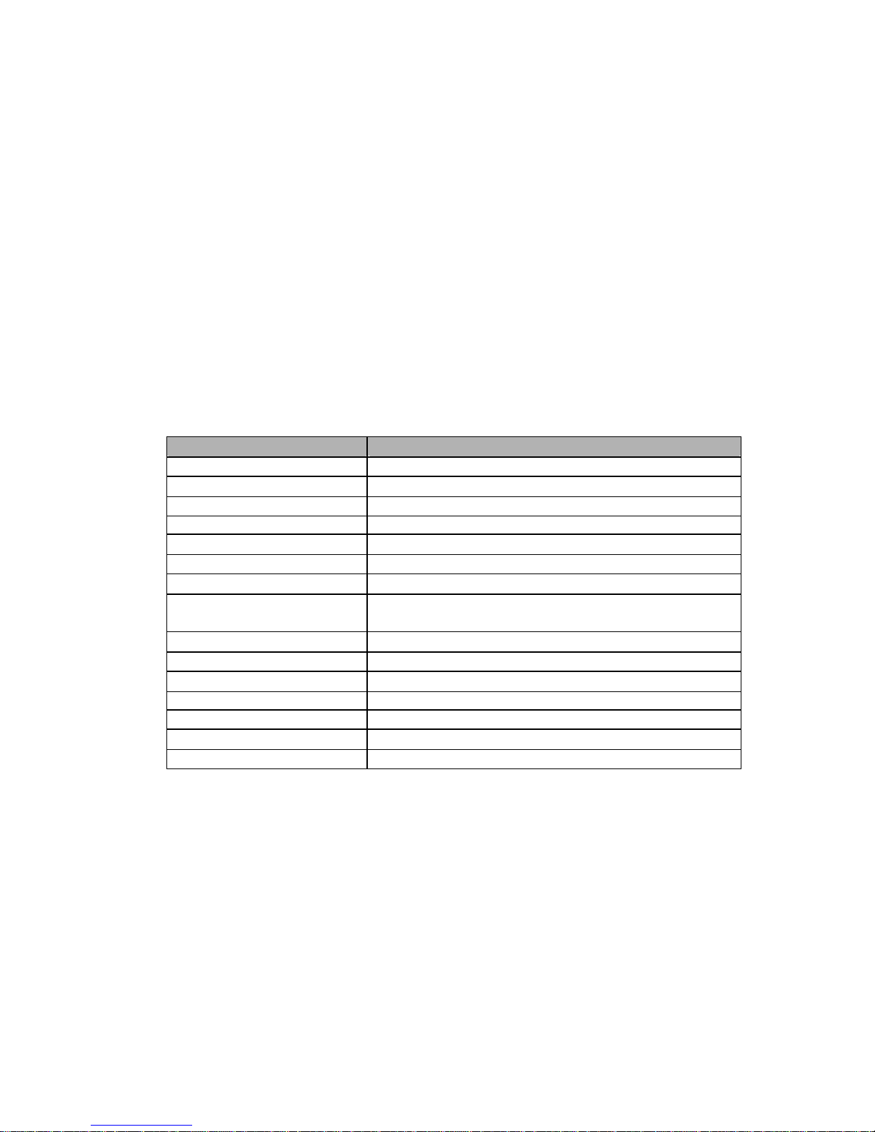
L2 Cache Size
Cache Size Data RAM Tag RAM Cacheable Size (8-bits tag)
512KB 64Kx32x2 32Kx8 128MB
L2 Cache Speed
Synchronous SRAM
Cache
Configuration 50MHz (tag/data) 60MHz (tag/data) 66MHz (tag/data)
Read 3-1-1-1
Write 3-1-1-115ns/12ns 12ns/9ns 12ns/9ns
DRAM Speed
The speed ratings of DRAM for various CPU external clock rates are listed below
(using 1Mx16 or 2Mx8 memory):
DRAM Speed 50MHz (clocks) 60MHz (clocks) 66MHz(clocks)
70ns read x-3-3-3read x-4-4-4read x-4-4-4
70ns write x-3-3-3write x-3-3-3write x-3-3-3
Refresh cycle (with CAS-BEFORE-RAS Refresh Cycle) = 2K

10
Super I/O Floppy Disk Controller -SMC FDC669FR
lIntelligent Auto Power Management
l16 Bit Address Qualification (Optional)
l2.88MB Super I/O Floppy Disk Controller
üSupport Vertical Recording Format
ü16 Byte Data FIFO
üEnhanced Digital Data Separator. Data rate up to 1Mb/s.
lMulti-Mode Parallel Port with ChiProtect Circuitry
üStandard Mode
IBM PC/AT and PS/2 compatible bi-directional Parallel port.
üEnhanced Mode
Enhanced Parallel Port (EPP) Compatible
üHigh Speed Mode
Microsoft and Hewlett Packard Extended Capabilities Port (ECP)
Compatible
lSerialPort
üTwo high speed NS16C550 compatible UARTs with Send/Receive 16
Byte FIFOs
üProgrammable Baud Rate Generator
üSupports 230K and 460K Baud
üModem Control Circuitry
üInfrared IrDA, HPSIR, ASKIR support

11
AIT1108E VGA to NTSC/PAL Converter
lConverts VGA source analog RGB into broadcast-quality NTSC or PAL video
signal.
lMultiple output standards-NTSC, PAL.
lS-Video output format.
Real PCI To USB (OHCI) Chip -CMD0670
lComplies with OpenHCI 1.0,USB 1.0,and PCI Local Bus 2.1 specifications.
lBridges PCI bus and the Universal Serial Bus (USB).
lUSB device bandwidth of up to 12 Mb/s.
lFull support of real time dynamic insertion and removal of devices.
l32-bit PCI local bus interface.
lPCI Bus Master.
lSupports up to 127 devices (concurrent operation).
lSupports all USB-compliant peripherals (e.g. keyboard, mouse, monitor,
telephone, joystick, etc)
lSupports legacy keyboards and mouse devices.
Keyboard Controller -Mitsubishi M38813M4
lTimers :8 bit prescaler X 2 + 8 bit timer X 3
lComparator :4 bit X 8 channels
lBus interface :2 bytes
lKey on wake-up :8 channels
lInterrupts :8 external,7 internal,and 1 software

12
ESS ES1879 High Quality Audio Chip
lSingle,mixed-signal,16-bit stereo VLSI chip for digital audio
lHigh-quality,20-voice ESFM music synthesizer patents pending
lSupports ES978 Expansion audio Mixer chip
lFull Plug and Play (PnP)
ES690 Wavetable Synthesizer
lWavetable music synthesizer.
lPlayback of 16-bit data at 44.1 KHz via the ES1xxx DAC.
lMIDI serial port compatible with MPU-401 serial port of ES1xxx.
lGlueless interface with the external wavetable ROM.
ES981 Wavetable ROM
l16-bit CMOS wavetable mask ROM.
l150 ns access time.
lTotal static operation.
lSingle +5V power supply requirement.
ES938 3-D Audio Effects Processor
lProvides Spatilizer 3-D stereo sound effects.
lExpands the sound stage of stereo and mono audio material for a fuller sound
environment from only two speakers.

13
Interfaces
Floppy Disk Drive Interface
Pin Description Pin Description
1VCC 29 N.C
2VCC 30 N.C
3MTR0# 31 N.C
4INDEX# 32 N.C
53MOD 33 N.C
6FDD0# 34 N.C
7TRK0# 35 N.C
8DSKCHG# 36 N.C
9HDSEL# 37 GND
10 DIR# 38 GND
11 RDATA# 39 N.C
12 STEP# 40 N.C
13 WRPRT# 41 N.C
14 WDATA# 42 N.C
15 WGATE# 43 N.C
16 DETECT0 44 N.C
17 GND 45 N.C
18 GND 46 N.C
19 N.C 47 N.C
20 DETECT1 48 N.C
21 N.C 49 N.C
22 N.C 50 N.C
23 N.C 51 N.C
24 N.C 52 N.C
25 N.C 53 N.C
26 N.C 54 N.C
27 N.C 55 VCC
28 N.C 56 VCC

14
Hard Disk Drive Interface
The Notebook PC has a standard PC/AT interface (IDE) which can directly interface
with any hard disk drive with an embedded controller supporting the same PC/AT
interface through the use of a 56-pin B/B connector. The 56-pin connector has the
following pin configurations:
Pin Description Pin Description
1VCC 29 SDD3
2VCC 30 SDD12
3N.C 31 SDD2
4N.C 32 SDD13
5N.C 33 SDD1
6N.C 34 SDD14
7N.C 35 SDD0
8N.C 36 SDD15
9N.C 37 GND
10 N.C 38 GND
11 N.C 39 HDDWRB#
12 N.C 40 N.C
13 N.C 41 HDDRDB#
14 N.C 42 N.C
15 N.C 43 CHRDYB
16 DETECT0 44 N.C
17 GND 45 IRQ15
18 GND 46 IO16#
19 IDERST# 47 HDDA1B
20 DETECT1 48 N.C
21 SDD7 49 HDDA0B
22 SDD8 50 HDDA2B
23 SDD6 51 HDDCS1B#
24 SDD9 52 HDDCS3B#
25 SDD5 53 HDD1#
26 SDD10 54 N.C
27 SDD4 55 VCC
28 SDD11 56 VCC

15
RS-232C Serial Interface
The Notebook PC has one RS-232C serial port which enables users to connect a
serial printer, a serial mouse, a plotter, a modem, etc. The key features of the serial
port are listed as follows:
üIBMPC/ATcompatible
ücompatiblewithNS16C550
üIndividual modem control/signals for each channel
üProgrammable serial interface characteristics :
*5-, 6-, 7-, or 8-bit characters
* Even, odd, or no parity bit generation and detection
* 1, 1 1/2 or 2 stop bit generation
* Tri-state TTL drives capabilities for bi-directional data bus and
control bus.
The RS-232C serial port uses a 9-pin D-sub male connector which has the following
pin configurations:
Pin Description
1DCD (DATA Carrier Detect)
2RXD (Received Data)
3TXD (Transmitted Data)
4DTR (Data Terminal Ready)
5GND (Signal Ground)
6DSR (Data Set Ready)
7RTS (Request To Send)
8CTS (Clear To Send)
9RI (Ring Indicator)
Parallel interface
The parallelinterface is implemented through using a 25-pin D-sub female connector
which has the following pin configurations:
Pin Description Pin Description
1Strobe# 2data 0
3Data 1 4Data 2
5Data 3 6Data 4
7Data 5 8Data 6
9Data 7 10 ACK#
11 Busy 12 PaperEmpty
13 Select 14 Auto Linefeed#
15 Error# 16 Initialize#
17 Select In 18 Ground
19 Ground 20 Ground
21 Ground 22 Ground
23 Ground 24 Ground
25 Ground

16
Expansion Memory Socket
The Notebook PC has two 144-pin SODIMM type Expansion memory sockets with
the following pin configurations:
Socket 1:
Pin Description Pin Description Pin Description
1GND 2GND 3MD0
4MD32 5MD1 6MD33
7MD2 8MD34 9MD3
10 MD35 11 MEM-VCC 12 MEM-VCC
13 MD4 14 MD36 15 MD5
16 MD37 17 MD6 18 MD38
19 MD7 20 MD39 21 GND
22 GND 23 ICAS#0 24 ICAS#4
25 ICAS#1 26 ICAS#5 27 MEM-VCC
28 MEM-VCC 29 IMA0 30 IMA3
31 IMA1 32 IMA4 33 IMA2
34 IMA5 35 GND 36 GND
37 MD8 38 MD40 39 MD9
40 MD41 41 MD10 42 MD42
43 MD11 44 MD43 45 MEM-VCC
46 MEM-VCC 47 MD12 48 MD44
49 MD13 50 MD45 51 MD14
52 MD46 53 MD15 54 MD47
55 GND 56 GND 57 N.C
58 N.C 59 N.C 60 N.C
61 MEMCLK1 62 CKE 63 MEM-VCC
64 MEM-VCC 65 SRAS# 66 SCAS#
67 IMWE# 68 N.C 69 IRAS#0
70 MEMCLK2 71 IRAS#1 72 N.C
73 GND 74 N.C 75 GND
76 GND 77 N.C 78 N.C
79 N.C 80 N.C 81 MEM-VCC
82 MEM-VCC 83 MD16 84 MD48
85 MD17 86 MD49 87 MD18
88 MD50 89 MD19 90 MD51
91 GND 92 GND 93 MD20
94 MD52 95 MD21 96 MD53
97 MD22 98 MD54 99 MD23
100 MD55 101 MEM-VCC 102 MEM-VCC
103 IMA6 104 IMA7 105 IMA8
106 IMA11 107 GND 108 GND
109 IMA9 110 IMA12 111 IMA10
112 N.C 113 MEM-VCC 114 MEM-VCC
115 ICAS#2 116 ICAS#6 117 ICAS#3
118 ICAS#7 119 GND 120 GND
121 MD24 122 MD56 123 MD25
124 MD57 125 MD26 126 MD58
127 MD27 128 MD59 129 MEM-VCC
130 MEM-VCC 131 MD28 132 MD60
133 MD29 134 MD61 135 MD30
136 MD62 137 MD31 138 MD63
139 GND 140 GND 141 SMBDA
142 SMBCL 143 MEM-VCC 144 MEM-VCC

17
Socket 2:
Pin Description Pin Description Pin Description
1GND 2GND 3MD0
4MD32 5MD1 6MD33
7MD2 8MD34 9MD3
10 MD35 11 MEM-VCC 12 MEM-VCC
13 MD4 14 MD36 15 MD5
16 MD37 17 MD6 18 MD38
19 MD7 20 MD39 21 GND
22 GND 23 ICAS#0 24 ICAS#4
25 ICAS#1 26 ICAS#5 27 MEM-VCC
28 MEM-VCC 29 IMA0 30 IMA3
31 IMA1 32 IMA4 33 IMA2
34 IMA5 35 GND 36 GND
37 MD8 38 MD40 39 MD9
40 MD41 41 MD10 42 MD42
43 MD11 44 MD43 45 MEM-VCC
46 MEM-VCC 47 MD12 48 MD44
49 MD13 50 MD45 51 MD14
52 MD46 53 MD15 54 MD47
55 GND 56 GND 57 N.C
58 N.C 59 N.C 60 N.C
61 MEMCLK3 62 CKE 63 MEM-VCC
64 MEM-VCC 65 SRAS# 66 SCAS#
67 IMWE# 68 N.C 69 IRAS#2
70 MEMCLK4 71 IRAS#3 72 N.C
73 GND 74 N.C 75 GND
76 GND 77 N.C 78 N.C
79 N.C 80 N.C 81 MEM-VCC
82 MEM-VCC 83 MD16 84 MD48
85 MD17 86 MD49 87 MD18
88 MD50 89 MD19 90 MD51
91 GND 92 GND 93 MD20
94 MD52 95 MD21 96 MD53
97 MD22 98 MD54 99 MD23
100 MD55 101 MEM-VCC 102 MEM-VCC
103 IMA6 104 IMA7 105 IMA8
106 IMA11 107 GND 108 GND
109 IMA9 110 IMA12 111 IMA10
112 N.C 113 MEM-VCC 114 MEM-VCC
115 ICAS#2 116 ICAS#6 117 ICAS#3
118 ICAS#7 119 GND 120 GND
121 MD24 122 MD56 123 MD25
124 MD57 125 MD26 126 MD58
127 MD27128 MD59 129 MEM-VCC
130 MEM-VCC 131 MD28 132 MD60
133 MD29 134 MD61 135 MD30
136 MD62 137 MD31 138 MD63
139 GND 140 GND 141 SMBDA
142 SMBCL 143 MEM-VCC 144 MEM-VCC

18
Docking Connector Pin Assignment
Pin Description Pin Description Pin Description
1A+ 2A+ 3CCO
4SOUTA 5GND 6/DCD2
7/DSR2 8SIN2 9/RTS2
10 GND 11 /STROBE 12 /AUTOFD
13 PPD0 14 /ERROR 15 PPD1
16 /INIT 17 PPD2 18 GND
19 SLCT 20 D-LOCK 21 CCLK3
22 GND 23 CCLK2 24 GND
25 CCLK1 26 GND 27 CCLK0
28 GND 29 A+ 30 CCO
31 CCO 32 +20V-EN 33 SINA
34 GND 35 SOUT2 36 /CTS2
37 /DTR2 38 /RI2 39 GND
40 /SLCTIN 41 PPD3 42 PPD4
43 PPD5 44 PPD6 45 PPD7
46 /ACK 47 BUSY 48 PE
49 BHSYNC 50 BVSYNC 51 GREEN
52 RED 53 BLUE 54 DDCCLK
55 DDCDATA 56 GND 57 GND
58 DSRA 59 RTSA 60 DTRA
61 DCDA 62 COMSTBY# 63 CAD31
64 CAD30 65 CAD19 66 CAD17
67 CC/BE#0 68 CC/BE#1 69 CGNT0#
70 CGNT1# 71 CREQ0# 72 CREQ1#
73 CAD15 74 CAD12 75 CAD9
76 CAD6 77 CAD3 78 CAD0
79 MTR0# 80 MTR1# 81 FDD0#
82 FDD1# 83 N.C 84 DOCKRDY#
85 FB0 86 DOCKEN# 87 CTSA
88 RIA 89 RI2 90 CINTA#
91 CINTB# 92 CAD29 93 CAD18
94 CAD16 95 CC/BE#2 96 CC/BE#3
97 CGNT2# 98 CGNT3# 99 CREQ2#
100 CREQ3# 101 CAD14 102 CAD11
103 CAD8 104 CAD5 105 CAD2
106 TRK0# 107 HDSEL# 108 RDATA#
109 WRPRT# 110 WGATE# 111 ENBL3V
112 DOCKEN# 113 DOCK-ON 114 SEL2
115 CINTC# 116 UN-DOCK# 117 CAD27
118 CAD25 119 CAD24 120 CAD22
121 CAD21 122 CIRDY# 123 CSTOP#
124 CSERR# 125 CPAR 126 CFRAME#
127 CBLOCK# 128 CDEVSEL# 129 CAD13
130 CAD10 131 CAD7 132 CAD4
133 CAD1 134 INDEX# 135 DSKCHG#
136 DIR# 137 STEP# 138 WDATA#
139 3MOD-B140 GND 141 N.C
142 SEL3 143 DOCK-VCC 144 CAD28
145 CAD26 146 GND 147 CAD23
148 GND 149 CAD20 150 GND
151 CPERR# 152 GND 153 CRST#
154 EN-722 155 CTRDY# 156 GND
157 MUS-DATA 158 MUS-CLK 159 KBD-DATA
160 KBD-CLK 161 XSD978 162 XSC978
163 978XA0 164 978XA1 165 978XA2
166 978XA3 167 GND 168 GND

19
Internal Trackpad Interface
There is a 8-pin connector used to interface with the internal trackpad. It will be
disabled when external mouse has been installed. The trackpadishardware-
connected to PS/2 port, hardware-compatible to Microsoft PS/2 mouse and software-
compatible to Microsoft mouse mode. The following is the pin configuration for the
connector:
Pin Description
1VCC
2PS/2 DATA
3PS/2 CLK
4SW Right
5SW Left
6GND
7N.C
8N.C
External Monitor Interface
Pin Description
1BRED
2BGREEN
3BBLUE
4N.C
5GND
6GND
7GND
8GND
9N.C
10 GND
11 N.C
12 DDCDATA
13 BHSYNC
14 BVSYNC
15 DDCCLK
RGB Out
Output Impedance: 75Ω
RGB peak voltage: 0.7Vpp

20
External Keyboard/PS2 Mouse Interface
Pin Description
1 KBD-DATA
2MUS-DATA
3GND
4VCC
5KBD-CLK
6MUS-CLK
External S-Video TV-Out Interface
Pin Description
1GND
2GND
3XLUMA
4XCRMA
External Game Port Interface
Pin Description
1VCC
2SWA
3TA
4GND
5GND
6TB
7SWB
8VCC
9VCC
10 SWC
11 TC
12 MSO
13 TD
14 SWD
15 MSI
This manual suits for next models
1
Table of contents
Other Clevo Laptop manuals