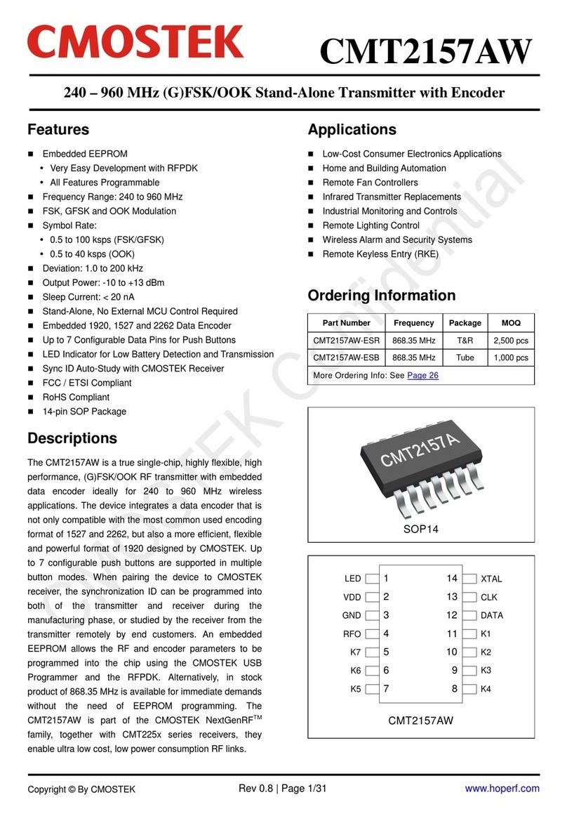
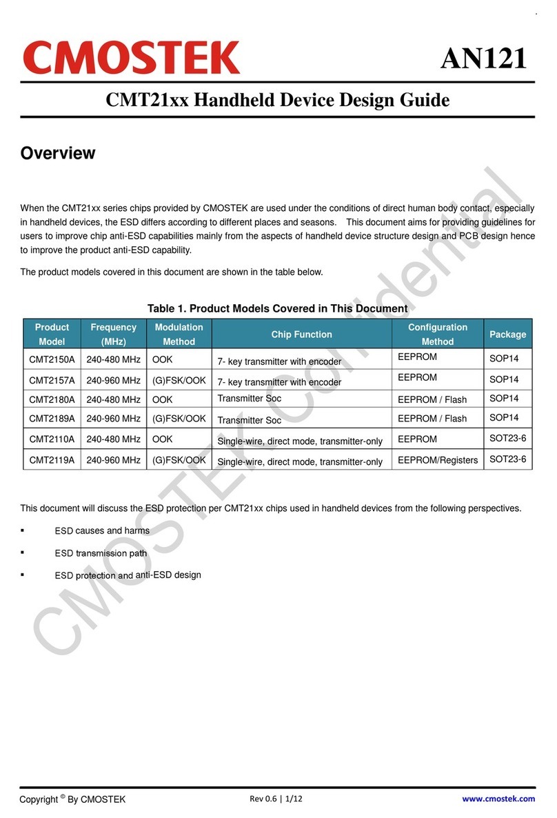
CMOSTEK CMT2150A User manual

CMT2150A
Rev 0.8 | Page 1/31
www.hoperf.com
CMT2150A
240 – 480 MHz OOK Stand-Alone Transmitter with Encoder
Copyright © By CMOSTEK
Features
Embedded EEPROM
Very Easy Development with RFPDK
All Features Programmable
Frequency Range: 240 to 480 MHz
Symbol Rate: 0.5 to 40 ksps
Output Power: -10 to +13 dBm
Current Consumption: 8.5 mA @ +10 dBm
Sleep Current: < 20 nA
Stand-Alone, No External MCU Control Required
Embedded 1920, 1527 and 2262 Data Encoder
Up to 7 Configurable Data Pins for Push Buttons
LED Indicator for Low Battery Detection and Transmission
Sync ID Auto-Study with CMOSTEK Receiver
FCC / ETSI Compliant
RoHS Compliant
14-pin SOP Package
Applications
Low-Cost Consumer Electronics Applications
Home and Building Automation
Remote Fan Controllers
Infrared Transmitter Replacements
Industrial Monitoring and Controls
Remote Lighting Control
Wireless Alarm and Security Systems
Remote Keyless Entry (RKE)
Descriptions
The CMT2150A is a true single-chip, highly flexible, high
performance, OOK RF transmitter with embedded data
encoder ideal for 240 to 480 MHz wireless applications.
The device integrates a data encoder that is not only
compatible with the most common used encoding format of
1527 and 2262, but also a more efficient, flexible and
powerful format of 1920 designed by CMOSTEK. Up to 7
configurable push buttons are supported in multiple button
modes. When pairing the device to CMOSTEK receiver,
the synchronization ID can be programmed into both of the
transmitter and receiver during the manufacturing phase,
or studied by the receiver from the transmitter remotely by
end customers. An embedded EEPROM allows the RF and
encoder parameters to be programmed into the chip using
the CMOSTEK USB Programmer and the RFPDK.
Alternatively, in stock product of 433.92 MHz is available
for immediate demands without the need of EEPROM
programming. The CMT2150A is part of the CMOSTEK
NextGenRFTM family, together with CMT225x series
receivers, they enable ultra low cost, low power
consumption RF links.
Ordering Information
Part Number Frequency Package
Option MOQ
CMT2150A-ESR 433.92 MHz T&R 2,500 pcs
CMT2150A-ESB 433.92 MHz Tube 1,000 pcs
More Ordering Info: See Page 26
1
2
3
4
5
6
7
14
13
12
10
9
8
11
LED
VDD
GND
RFO
K7
K6
K5
XTAL
CLK
DATA
K1
K2
K3
K4
CMT2150A
SOP14
CMT2150A
Rev 0.8 | Page 2/31
www.hoperf.com
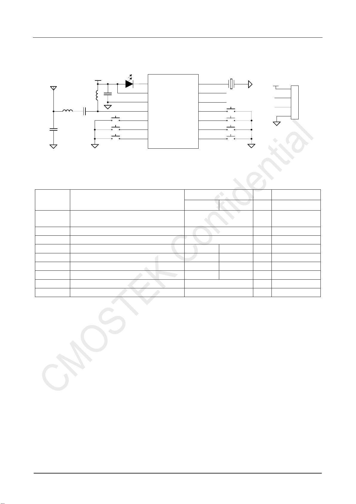
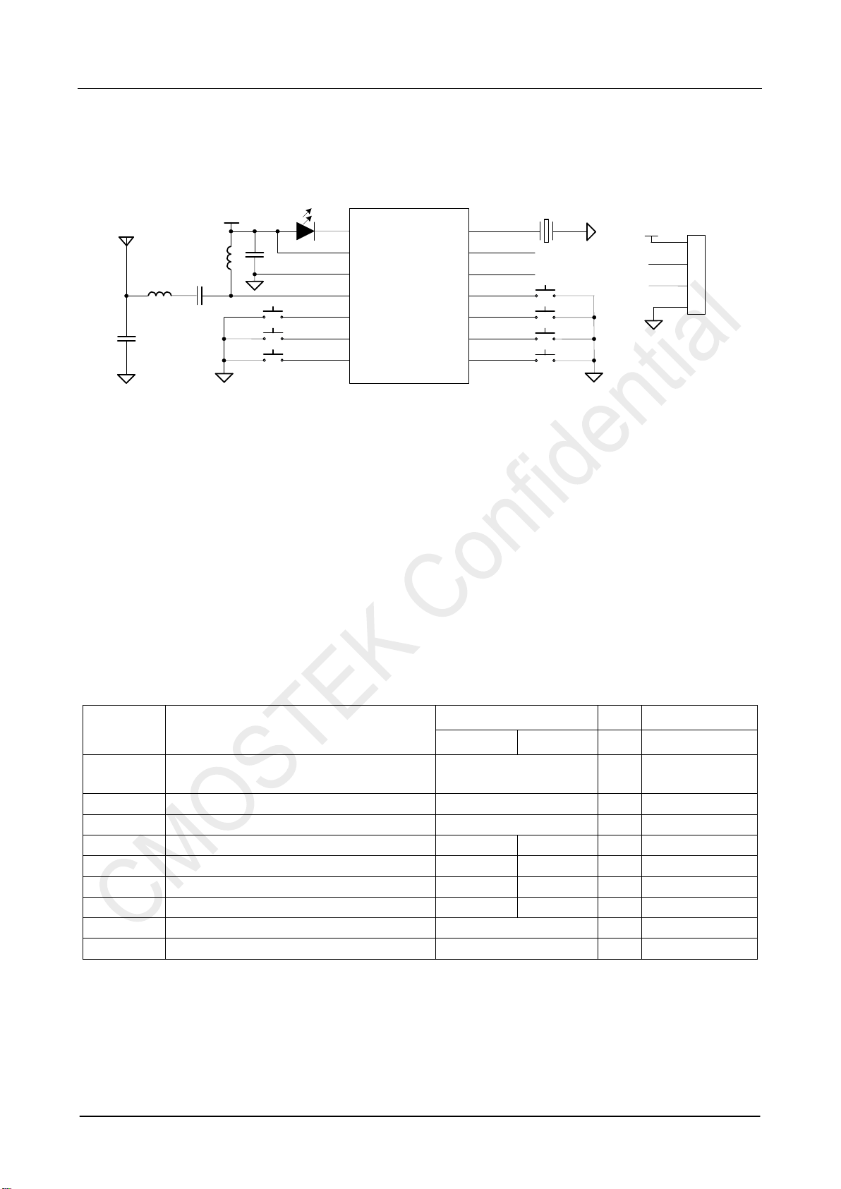
Typical Application
ANT VDD
U1
C2
L2 C1
L1 C0
SW7
SW6
SW5
LED
VDD
GND
RFO
K7
K6
K5
1
2
3
4
5
6
7
D1
8
9
10
11
12
13
14
SW4
SW3
SW2
SW1
XTAL
CLK
DATA
K1
K2
K3
K4
X1
CLK
DATA
CLK
DATA
J1
1
2
3
4
VDD
CMT2150A
Note: Connector J1 is for
EEPROM Programming
Figure 1. CMT2150A Typical Application Schematic
Table 1. BOM of 315/433.92 MHz Typical Application
Designator Descriptions Value
Unit Manufacturer
315 MHz
433.92 MHz
U1 CMT2150A, 240 – 480 MHz OOK stand-alone
transmitter with encoder
- - CMOSTEK
X1 ±20 ppm, SMD32*25 mm crystal 26 MHz EPSON
C0 ±20%, 0402 X7R, 25 V 0.1 uF Murata GRM15
C1 ±5%, 0402 NP0, 50 V 82 82 pF Murata GRM15
C2 ±5%, 0402 NP0, 50 V 9.1 9.1 pF Murata GRM15
L1 ±5%, 0603 multi-layer chip inductor 180 180 nH Murata LQG18
L2 ±5%, 0603 multi-layer chip inductor 39 22 nH Murata LQG18
D1 D0603, red LED - - -
SW[7:1] Push buttons - - -

CMT2150A
Rev 0.8 | Page 3/31
www.hoperf.com
Abbreviations
Abbreviations used in this data sheet are described below
AN Application Notes OOK On-Off Keying
BOM
Bill of Materials
PA
Power Amplifier
BSC Basic Spacing between Centers PC Personal Computer
BW
Bandwidth
PCB
Printed Circuit Board
DC Direct Current PLL Phase Lock Loop
EEPROM Electrically Erasable Programmable Read-Only
Memory
PN
Phase Noise
RBW Resolution Bandwidth
ESD
Electro-Static Discharge
RCLK
Reference Clock
ESR Equivalent Series Resistance RF Radio Frequency
GUI
Graphical User Interface
RFPDK
RF Product Development Kit
IC Integrated Circuit RoHS Restriction of Hazardous Substances
LDO
Low Drop-Out
Rx
Receiving, Receiver
Max Maximum SOT Small-Outline Transistor
MCU
Microcontroller Unit
TBD
To Be Determined
Min Minimum Tx Transmission, Transmitter
MOQ
Minimum Order Quantity
Typ
Typical
NP0 Negative-Positive-Zero XO/XOSC Crystal Oscillator
OBW
Occupied Bandwidth
XTAL
Crystal

CMT2150A
Rev 0.8 | Page 4/31
www.hoperf.com
Table of Contents
1. Electrical Characteristics............................................................................................................................................ 5
1.1 Recommended Operating Conditions...................................................................................................................5
1.2 Absolute Maximum Ratings................................................................................................................................... 5
1.3 Transmitter Specifications.....................................................................................................................................6
1.4Crystal Oscillator...................................................................................................................................................7
2. Pin Descriptions .......................................................................................................................................................... 8
3. Typical Performance Characteristics......................................................................................................................... 9
4. Typical Application Schematics............................................................................................................................... 10
4.1 Low-Cost Application Schematic......................................................................................................................... 10
4.2 FCC/ETSI Compliant Application Schematic....................................................................................................... 11
5. Functional Descriptions............................................................................................................................................ 12
5.1 Overview............................................................................................................................................................. 12
5.2 Modulation, Frequency and Symbol Rate........................................................................................................... 12
5.3 Embedded EEPROM and RFPDK...................................................................................................................... 13
5.4 Power Amplifier................................................................................................................................................... 15
5.5 PA Ramping........................................................................................................................................................ 15
5.6 Working States.................................................................................................................................................... 16
5.7 The Encoder........................................................................................................................................................ 17
5.7.1 1920 Packet Structure............................................................................................................................................17
5.7.2 1527 Packet Structure............................................................................................................................................18
5.7.32262 Packet Structure............................................................................................................................................19
5.8 ID Study.............................................................................................................................................................. 20
5.9 Button Modes...................................................................................................................................................... 20
5.9.1 Normal......................................................................................................................................................................20
5.9.2 Matrix........................................................................................................................................................................21
5.9.3 Toggle.......................................................................................................................................................................22
5.9.4 PWM.........................................................................................................................................................................23
5.10 LED Driving Capability........................................................................................................................................ 24
5.11 Low Battery Detection (LBD)............................................................................................................................... 24
5.12 Crystal Oscillator and RCLK................................................................................................................................ 24
6. Ordering Information................................................................................................................................................. 26
7. Package Outline......................................................................................................................................................... 27
8. Top Marking ............................................................................................................................................................... 28
8.1 CMT2150A Top Marking..................................................................................................................................... 28
9. Other Documentations.............................................................................................................................................. 29
10.Document Change List.............................................................................................................................................. 30
11. Contact Information .................................................................................................................................................. 31
CMT2150A
Rev 0.8 | Page 5/31
www.hoperf.com
1. Electrical Characteristics
VDD = 3.3 V, TOP = 25 ℃, FRF = 433.92 MHz, output power is +10 dBm terminated in a matched 50 Ω impedance, unless
otherwise noted.
1.1 Recommended Operating Conditions
Table 2. Recommended Operation Conditions
Parameter Symbol Conditions Min Typ Max Unit
Operation Voltage Supply VDD
1.8 3.6 V
Operation Temperature TOP
-40 85 ℃
Supply Voltage Slew Rate 1mV/us
1.2 Absolute Maximum Ratings
Table 3. Absolute Maximum Ratings[1]
Parameter Symbol Conditions Min Max Unit
Supply Voltage VDD
-0.3 3.6 V
Interface Voltage VIN
-0.3 VDD + 0.3 V
Junction Temperature TJ-40 125 ℃
Storage Temperature TSTG
-50 150 ℃
Soldering Temperature TSDR Lasts at least 30 seconds 255 ℃
ESD Rating Human Body Model (HBM) -2 2 kV
Latch-up Current @ 85 ℃-100 100 mA
Note:
[1]. Stresses above those listed as “absolute maximum ratings” may cause permanent damage to the device. This is a stress
rating only and functional operation of the device under these conditions is not implied. Exposure to maximum rating
conditions for extended periods may affect device reliability.
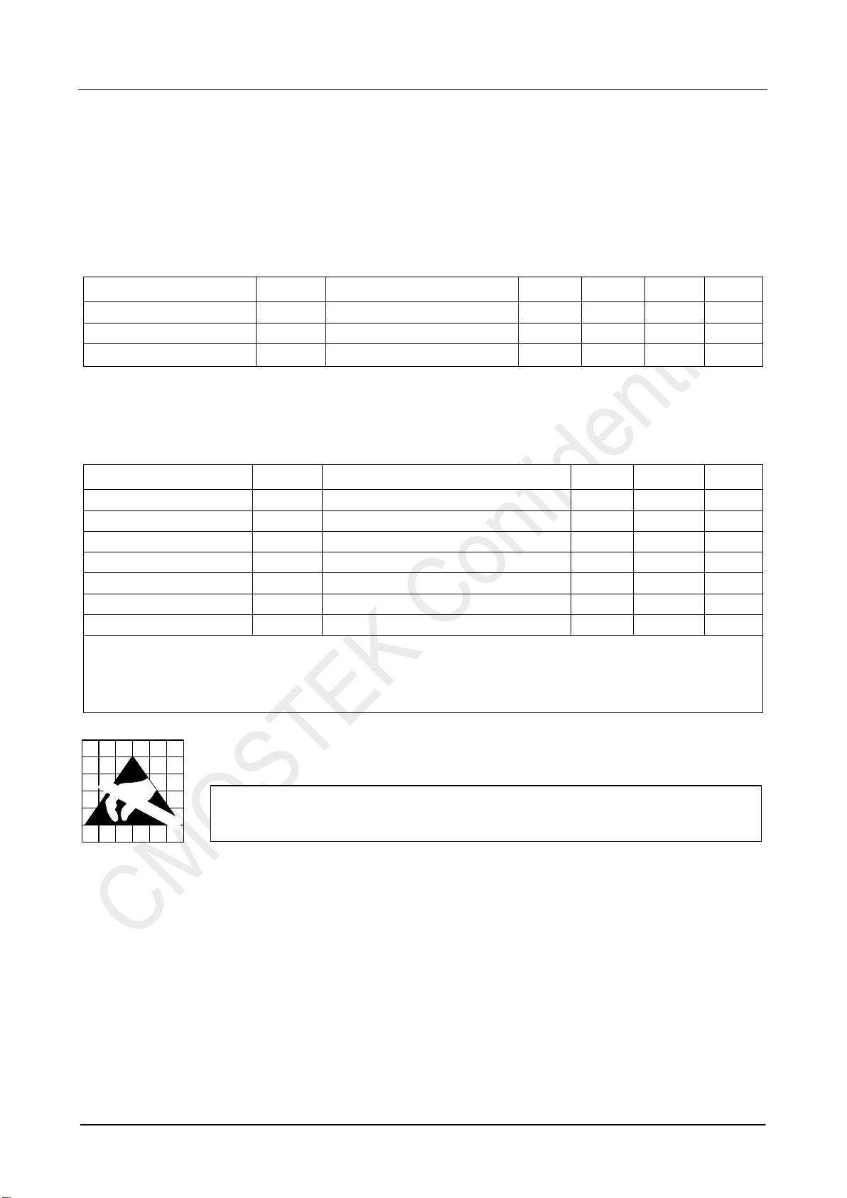
Caution! ESD sensitive device. Precaution should be used when handling the device in order
to prevent permanent damage.

CMT2150A
Rev 0.8 | Page 6/31
www.hoperf.com
1.3 Transmitter Specifications
Table 4. Transmitter Specifications
Parameter Symbol Conditions Min Typ Max Unit
Frequency Range[1] FRF 240 480 MHz
Synthesizer Frequency
Resolution FRES 198 Hz
Maximum Output Power POUT(Max) +13 dBm
Minimum Output Power POUT(Min) -10 dBm
Output Power Step Size PSTEP 1dB
PA Ramping Time[2] tRAMP 01024 us
Current Consumption[3]
@ 315 MHz IDD-315
0 dBm 5.9 mA
+10 dBm 8.1 mA
+13 dBm 8.8 mA
Current Consumption [3]
@ 433.92 MHz IDD-433.92
0 dBm, 6 mA
+10 dBm 8.5 mA
+13 dBm 10.2 mA
Sleep Current ISLEEP 20 nA
Symbol Rate SR 0.5 40 ksps
Frequency Tune Time tTUNE From XO stable to ready to transmit,
include the frequency calibration
370 us
Phase Noise PN
100 kHz offset from FRF -80 dBc/Hz
200 kHz offset from FRF -81 dBc/Hz
400 kHz offset from FRF -91 dBc/Hz
600 kHz offset from FRF -96 dBc/Hz
1.2 MHz offset from FRF -108dBc/Hz
Harmonics Output for 315
MHz[4] H2315 2nd harm @ 630 MHz, +13 dBm POUT -60 dBm
H3315 3rd harm @ 945 MHz, +13 dBm POUT -65 dBm
Harmonics Output for
433.92 MHz[4] H2433.92 2nd harm @ 867.84 MHz, +13 dBm POUT -52 dBm
H3433.92 3rd harm @ 1301.76 MHz, +13 dBm POUT -57 dBm
OOK Extinction Ration 60 dB
Occupied Bandwidth @
315 MHz FOBW315 Measured @ -20 dBc, RBW = 1 kHz, SR =
1.2 ksps, tRAMP = 256 us 6kHz
Occupied Bandwidth @
433.92 MHz
FOBW433.92 Measured @ -20 dBc, RBW = 1 kHz, SR =
1.2 ksps, tRAMP = 256 us
7kHz
Notes:
[1]. The frequency range is continuous over the specified range.
[2]. 0 and 2nus, n = 0 to 10, when set to “0”, the PA output power will ramp to its configured value in the shortest possible
time.
[3]. The working currents are tested with: 1527 packet format/Normal button mode/ 4 push buttons/Sync ID = 0/No LED.
[4]. The harmonics output is measured with the application shown as Figure 10.

CMT2150A
Rev 0.8 | Page 7/31
www.hoperf.com
1.4 Crystal Oscillator
Table 5. Crystal Oscillator Specifications
Parameter Symbol Conditions Min Typ Max Unit
Crystal Frequency[1] FXTAL 26 26 26 MHz
Crystal Tolerance[2] ±20 ppm
Load Capacitance[3] CLOAD
12
20 pF
Crystal ESR Rm 60 Ω
XTAL Startup Time[4] tXTAL 400 us
Notes:
[1]. The CMT2150A can directly work with external 26 MHz reference clock input to XTAL pin (a coupling capacitor is
required) with amplitude 0.3 to 0.7 Vpp.
[2]. This is the total tolerance including (1) initial tolerance, (2) crystal loading, (3) aging, and (4) temperature dependence.
The acceptable crystal tolerance depends on RF frequency and channel spacing/bandwidth.
[3]. The required crystal load capacitance is integrated on-chip to minimize the number of external components.
[4]. This parameter is to a large degree crystal dependent.

CMT2150A
Rev 0.8 | Page 8/31
www.hoperf.com
2. Pin Descriptions
1
2
3
4
5
6
7
14
13
12
10
9
8
11
LED
VDD
GND
RFO
K7
K6
K5
XTAL
CLK
DATA
K1
K2
K3
K4
Figure 2. CMT2150A Pin Assignments
Table 6. CMT2150A Pin Descriptions
Pin Number Name I/O Descriptions
1 LED O LED driver, active low
2 VDD I Power supply input
3 GND I Ground
4 RFO O Power amplifier output
5 - 11 K[7:1] I Push button 7 to 1
12 DATA IO Data pin to access the embedded EEPROM, internally pulled up to VDD
13 CLK I Clock pin to access the embedded EEPROM, internally pulled up to VDD
14 XTAL I 26 MHz single-ended crystal oscillator input or
External 26 MHz reference clock input

CMT2150A
Rev 0.8 | Page 9/31
www.hoperf.com
3. Typical Performance Characteristics
13.4dBm
@ 433.92 MHz
-56.8 dBm
@ 435.12 MHz
-60
-50
-40
-30
-20
-10
0
10
20
432.42 432.72 433.02 433.32 433.62 433.92 434.22 434.52 434.82 435.12 435.42
Power(dBm)
Frequency (MHz)
Phase Noise
13.6 dBm
@ 433.92 MHz
-52.0 dBm
@ 867.84 MHz
-70
-60
-50
-40
-30
-20
-10
0
10
20
250 365 480 595 710 825 940 1055 1170 1285 1400
Power (dBm)
Frequency (MHz) (RBW = 10 kHz)
Harmonics of 433.92 MHz
-57 dBm
@1301.76
MHz
-90
-80
-70
-60
-50
1301.72 1301.75 1301.78 1301.81
Power(dBm)
Freq (MHz) (RBW =1 kHz)
3rd Harmonic
-60
-50
-40
-30
-20
-10
0
10
20
432.92 433.12 433.32 433.52 433.72 433.92 434.12 434.32 434.52 434.72 434.92
Power(dBm)
Frequency (MHz)
OOK Spectrum
-50
-40
-30
-20
-10
0
10
433.17 433.37 433.57 433.77 433.97 434.17 434.37 434.57
Power (dBm)
Frequency (MHz)
Spectrum of Various PA Ramping Options
128 us
64 us
32 us
16 us
8 us
4 us
-50
-40
-30
-20
-10
0
10
433.17 433.37 433.57 433.77 433.97 434.17 434.37 434.57
Power (dBm)
Frequency (MHz)
Spectrum of Various PA Ramping Options
1024 us
512 us
256 us
128 us
64 us
32 us
SR= 1.2 ksps
-2
0
2
4
6
8
10
12
14
16
1.6 1.8 22.2 2.4 2.6 2.8 33.2 3.4 3.6 3.8
Power (dBm)
SupplyVoltage (V)
POUT vs. VDD
13dBm
10dBm
0dBm
Figure 4. Harmonics of 433.92 MHz,
POUT = +13 dBm
Figure 5. OOK Spectrum,
POUT = +10 dBm, tRAMP = 32 us
Figure 6. Spectrum of PA Ramping,
SR = 9.6 ksps, POUT = +10 dBm
Figure 8. Spectrum of PA Ramping,
SR = 1.2 ksps, POUT = +10 dBm
Figure 3. Phase Noise, FRF = 433.92 MHz,
POUT = +13 dBm, RBW = 10 kHz, Un-encoded
Figure 7. Output Power vs. Supply
Voltages, FRF = 433.92 MHz
CMT2150A
Rev 0.8 | Page 10/31
www.hoperf.com
4. Typical Application Schematics
4.1 Low-Cost Application Schematic
ANT VDD
U1
C2
L2 C1
L1 C0
SW7
SW6
SW5
LED
VDD
GND
RFO
K7
K6
K5
1
2
3
4
5
6
7
D1
8
9
10
11
12
13
14
SW4
SW3
SW2
SW1
XTAL
CLK
DATA
K1
K2
K3
K4
X1
CLK
DATA
CLK
DATA
J1
1
2
3
4
VDD
CMT2150A
Note: Connector J1 is for
EEPROM Programming
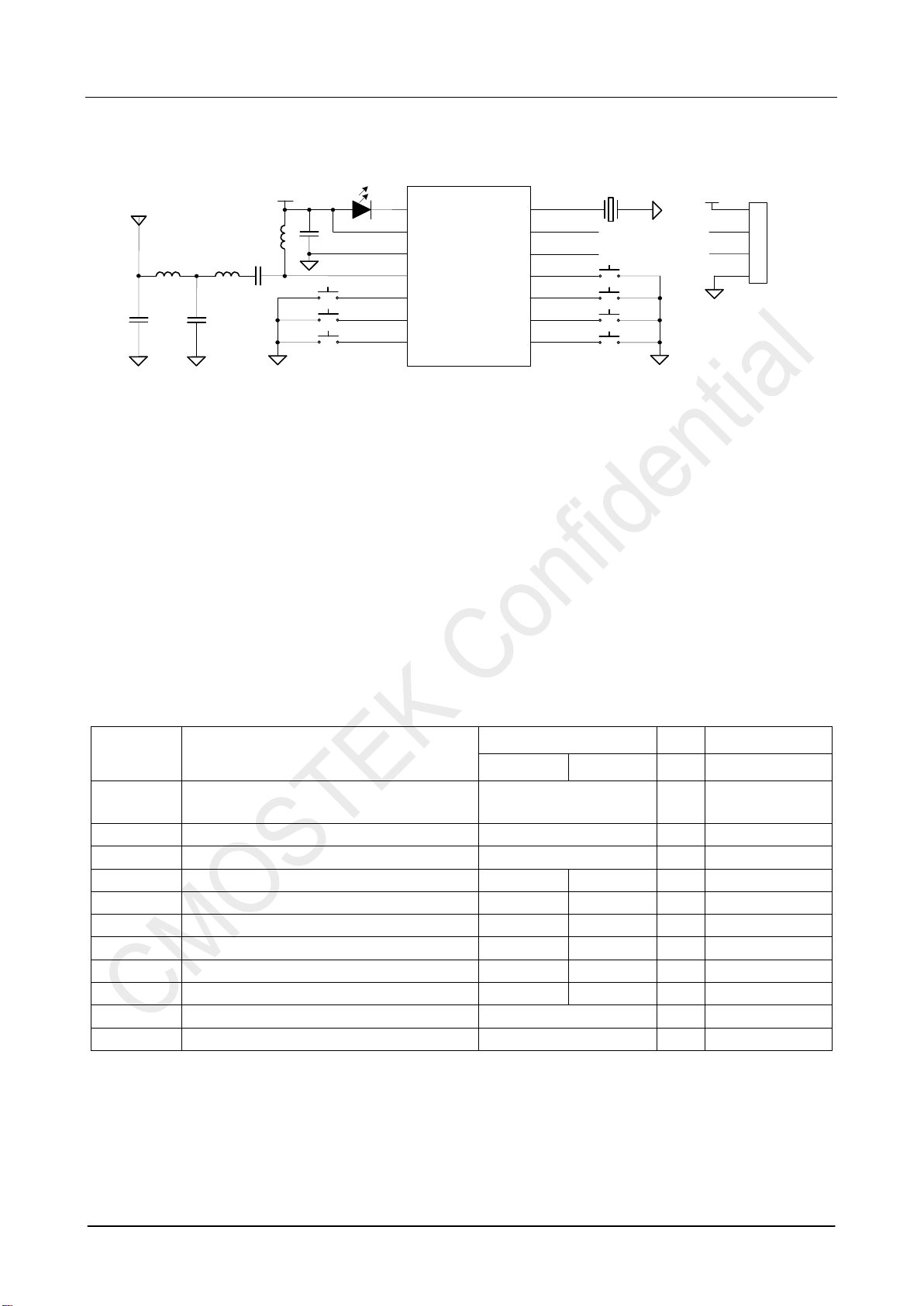
Figure 9. Low-Cost Application Schematic
Notes:
1. Connector J1 is a must for the CMT2150A EEPROM access during development or manufacture phase.
2. The general layout guidelines are listed below. For more design details, please refer to “AN111 CMT215x Schematic and
PCB Layout Design Guideline”
Use as much continuous ground plane metallization as possible.
Use as many grounding vias (especially near to the GND pins) as possible to minimize series parasitic inductance
between the ground pour and the GND pins.
Avoid using long and/or thin transmission lines to connect the components.
Avoid placing the nearby inductors in the same orientation to reduce the coupling between them.
Place C0 as close to the CMT2150A as possible for better filtering.
3. The table below shows the BOM of 315/433.92 MHz Low-Cost Application. For the BOM of more applications, please
refer to “AN111 CMT215x Schematic and PCB Layout Design Guideline”.
Table 7. BOM of 315/433.92 MHz Low-Cost Application
Designator Descriptions Value
Unit Manufacturer
315 MHz
433.92 MHz
U1 CMT2150A, 240 – 480 MHz OOK stand-alone
transmitter with encoder - - CMOSTEK
X1 ±20 ppm, SMD32*25 mm crystal 26 MHz EPSON
C0 ±20%, 0402 X7R, 25 V 0.1 uF Murata GRM15
C1 ±5%, 0402 NP0, 50 V 82 82 pF Murata GRM15
C2 ±5%, 0402 NP0, 50 V 9.1 9.1 pF Murata GRM15
L1 ±5%, 0603 multi-layer chip inductor 180 180 nH Murata LQG18
L2 ±5%, 0603 multi-layer chip inductor 39 22 nH Murata LQG18
D1 D0603, red LED - - -
SW[7:1] Push buttons - - -
CMT2150A
Rev 0.8 | Page 11/31
www.hoperf.com
4.2 FCC/ETSI Compliant Application Schematic
VDD
U1
C2
L2 C1
L1 C0
SW7
SW6
SW5
LED
VDD
GND
RFO
K7
K6
K5
1
2
3
4
5
6
7
D1
8
9
10
11
12
13
14
SW4
SW3
SW2
SW1
XTAL
CLK
DATA
K1
K2
K3
K4
X1
CLK
DATA
CMT2150A
ANT
L3
C3
CLK
DATA
J1
1
2
3
4
VDD
Note: Connector J1 is for
EEPROM Programming
Figure 10. FCC/ETSI Compliant Application Schematic
Notes:
1. Connector J1 is a must for the CMT2150A EEPROM access during development or manufacture phase.
2. The general layout guidelines are listed below. For more design details, please refer to “AN111 CMT215x Schematic and
PCB Layout Design Guideline”.
Use as much continuous ground plane metallization as possible.
Use as many grounding vias (especially near to the GND pins) as possible to minimize series parasitic inductance
between the ground pour and the GND pins.
Avoid using long and/or thin transmission lines to connect the components.
Avoid placing the nearby inductors in the same orientation to reduce the coupling between them.
Place C0 as close to the CMT2150A as possible for better filtering.
3. The table below shows the BOM of 315/433.92 MHz FCC/ETSI Compliant Application. For the BOM of more application,
please refer to “AN111 CMT215x Schematic and PCB Layout Design Guideline”.
Table 8. BOM of 315/433.92 MHz FCC/ETSI Compliant Application
Designator Descriptions Value
Unit Manufacturer
315 MHz
433.92 MHz
U1 CMT2150A, 240 – 480 MHz OOK stand-alone
transmitter with encoder - CMOSTEK
X1 ±20 ppm, SMD32*25 mm crystal 26 MHz EPSON
C0 ±20%, 0402 X7R, 25 V 0.1 uF Murata GRM15
C1
±5%, 0402 NP0, 50 V
68
68
pF
Murata GRM15
C2 ±5%, 0402 NP0, 50 V 18 15 pF Murata GRM15
C3 ±5%, 0402 NP0, 50 V 15 15 pF Murata GRM15
L1
±5%, 0603 multi-layer chip inductor
180
180
nH
Murata LQG18
L2 ±5%, 0603 multi-layer chip inductor 51 36 nH Murata LQG18
L3 ±5%, 0603 multi-layer chip inductor 27 18 nH Murata LQG18
D1 D0603, red LED - - -
SW[7:1] Push buttons - - -

CMT2150A
Rev 0.8 | Page 12/31
www.hoperf.com
5. Functional Descriptions
Modulator
LDOs
VDD
GND
CLK
DATA
XTAL RFO
Loop
Filter
PFD/CP
Frac-N DIV
Encoder Ramp-control
Interface & Control Logics
EEPROM
POR
PA
VCOXOSC
Bandgap LED Driver LED
K[7:1]
Figure 11. CMT2150A Functional Block Diagram
5.1 Overview
The CMT2150A is a true single-chip, highly flexible, high performance, OOK RF transmitter with embedded data encoder ideal
for 240 to 480 MHz wireless applications. It is part of the CMOSTEK NextGenRFTM family, which includes a complete line of
transmitters, receivers and transceivers. The device integrates a data encoder that is not only compatible with the most
common used encoding format of 1527 and 2262, but also a more efficient, flexible and powerful format of 1920 designed by
CMOSTEK. Up to 7 configurable push buttons are supported in multiple button modes. The device is optimized for the low
system cost, low power consumption, battery powered application with its highly integrated and low power design.
The functional block diagram of the CMT2150A is shown in figure above. The CMT2150A is based on direct synthesis of the
RF frequency by means of a fully integrated low-noise fractional-N frequency synthesizer. It uses a 1-pin crystal oscillator
circuit with the required crystal load capacitance integrated on-chip to minimize the number of external components. Every
analog block is calibrated on each Power-on Reset (POR) to an internal reference voltage source. The calibration can help the
chip to finely work under different temperatures and supply voltages. The transmission is triggered by pressing the push
button(s). The data is modulated and sent out by a highly efficient PA which output power can be configured from -10 to +13
dBm in 1 dB step size. RF Frequency, PA output power and other product features can be programmed into the embedded
EEPROM by the RFPDK and USB Programmer.This saves the cost and simplifies the product development and
manufacturing effort. Alternatively, in stock product of 433.92 MHz is available for immediate demands without the need of
EEPROM programming. The CMT2150A operates from 1.8 to 3.6 V so that it can finely work with most batteries to their useful
power limits. It only consumes 8.5 mA when transmitting +10 dBm power at 433.92 MHz under 3.3 V supply voltage.
5.2 Modulation, Frequency and Symbol Rate
The CMT2150A supports OOK modulation with the symbol rate up to 40 ksps. It continuously covers the frequency range from
240 to 480 MHz, including the license free ISM frequency band around 315 MHz and 433.92 MHz. The device contains a high
spectrum purity low power fractional-N frequency synthesizer with output frequency resolution better than 198 Hz. See Table 9
for the modulation, frequency and symbol rate specifications.
CMT2150A
Rev 0.8 | Page 13/31
www.hoperf.com
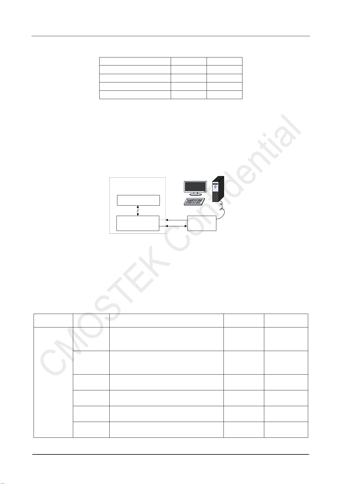
Table 9. Modulation, Frequency and Symbol Rate
Parameter
Value
Unit
Modulation OOK -
Frequency 240 to 480 MHz
Frequency Resolution 198 Hz
Symbol Rate 0.5 to 40 ksps
5.3 Embedded EEPROM and RFPDK
The RFPDK (RF Products Development Kit) is a very user-friendly software tool delivered for the user configuring the
CMT2150A in the most intuitional way. The user only needs to fill in/select the proper value of each parameter and click the
“Burn” button to complete the chip configuration. No register access and control is required in the application program. See
figure below for the accessing of the EEPROM and Table 10 for the summary of all the configurable parameters of the
CMT2150A on the RFPDK.
CMT2150A
Interface
CMOSTEK USB
Programmer
CLK
DATA
RFPDK
EEPROM
Figure 12. Accessing Embedded EEPROM
For more details of the CMOSTEK USB Programmer and the RFPDK, please refer to “AN113 CMT2150A/2250(1)A One-Way
RF Link Development Kits User’s Guide”. For the detail of CMT2150A configurations with the RFPDK, please refer to “AN112
CMT2150A Configuration Guideline”.
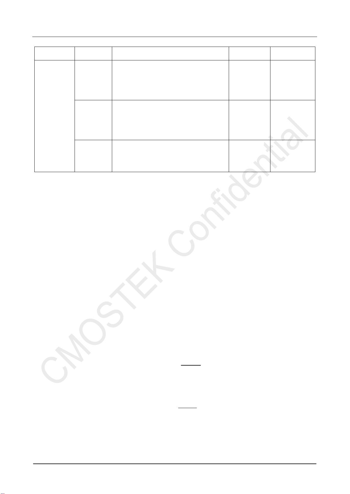
Table 10. Configurable Parameters in RFPDK
Category Parameters Descriptions Default Mode
RF Settings
Frequency To input a desired transmitting radio frequency in
the range from 240 to 480 MHz. The step size is
0.001 MHz. 433.92 MHz Basic
Advanced
Tx Power To select a proper transmitting output power from
-10 dBm to +14 dBm, 1 dBm margin is given
above +13 dBm. +13 dBm Basic
Advanced
Xtal Cload On-chip XOSC load capacitance options: from 10
to 22 pF.
15.00 pF Basic
Advanced
Symbol Rate To determines the symbol rate of the transmitted
data: from 0.5 to 40 ksps. 4.8 Basic
Advanced
PA Ramping To control PA output power ramp up/down time,
options are 0 and 2
n
us (n from 0 to 10).
0 us Advanced
LED Driving
Capability This defines the driving current of the LED pin.
The options are: Disable, 5, 10, 15 or 20 mA. 5 mA Advanced

CMT2150A
Rev 0.8 | Page 14/31
www.hoperf.com
Category Parameters Descriptions Default Mode
LBD
Threshold
This defines the Low Battery Detection threshold.
The options are: Disable, 1.7, 1.8, 1.9, 2.0, 2.1,
2.2, 2.3, 2.4, 2.5, 2.6, 2.7 or 2.8 V. 2.4 V Advanced
Encoder
Settings
Encoder
Select the packet encoding format, the options
are: 1920, 1527 and 2262. See Table 13, Table 14
and Table 15 for the configurable parameters in
each packet.
1527 Basic
Advanced
Bit Format
This tells the device how many symbols are used
to construct a single bit in the 1920 mode. The
options are: 3, 4, 5 or 6 sym/bit. The Bit Format is
fixed at 4 sym/bit in 1527 mode and 8 sym/bit in
2262 mode. It is only available in 1920 mode.
3 Basic
Advanced
Number of
Packets
This defines the minimum number of packet(s)
being transmitted during each button pressing
action. It also defines the number of packet(s)
being transmitted during each periodic
transmission. The range is from 1 to 256.
1 Advanced
Packet
Interval
This defines the time interval amount two
consecutive transmitted packets. The unit is in
symbol, the range is from 0 to 255 symbols of
zero.
0 symbols of
zero Basic
Advanced
Push Button
Settings
Button Mode
Select the button encoding mode, the options are:
Normal, Matrix, Toggle and PWM. For 1920 and
1527 format, all these button modes are
supported; For 2262 format, only Normal button
mode is supported.
Normal Basic
Advanced
On/Off
Button(s)
Select the numbers of on/off button for Toggle and
PWM button modes, the options are: Single or
Separated. Single Basic
Advanced
Number of
Button(s)
This option is only available in Normal Button
Mode, and Encoder is set to 1920 and 1527. It
defines the number of activated button(s) to be
used in the application. The range is from 1 to 7.
4 Basic
Advanced
Data
Inversion
Allow the user to select whether or not to inverse
the transmitted data bits values in the Normal and
Toggle Button Mode. The options are: No or Yes. No Advanced
Periodic
Transmission Turn on/off the periodic transmission mode of the
device. The options are: On or Off. Off Advanced
Periodic Time
This parameter is only available when Periodic
Transmission is turned on. It defines the periodic
time for transmitting a fixed set of data. The range
is from 2 to 7683.512 s, accurate to 3 decimal
points. It is only available when Periodic
Transmission is on.
1.000 s Advanced
Study Settings ID Study Turn on/off the Sync ID study function, the options
are: On or Off. The ID Study is only supported in
1920 and 1527 mode. Off Advanced
CMT2150A
Rev 0.8 | Page 15/31
www.hoperf.com
Category Parameters Descriptions Default Mode
Study Trigger
Time
This parameter is only available when ID Study is
turned on. It defines the time from the instance of
pressing the study button to the instance at which
the device starts to transmit the study packets.
The range is from 1 to 15 second(s).
5 s Advanced
Study Button
This parameter is only available when ID Study is
turned on. It defines which button is used to trigger
the transmission of the study packets. The options
are the current buttons used in the Push Button
Settings.
Pin 11 (K1) Advanced
Study Power
This parameter is only available when ID Study is
turned on. It defines the PA power when the
device is transmitting the study packets. The
range is from –10 to +14 dBm.
-6 dBm Basic
Advanced
5.4 Power Amplifier
A highly efficient single-ended Power Amplifier (PA) is integrated in the CMT2150A to transmit the modulated signal out.
Depending on the application, the user can design a matching network for the PA to exhibit optimum efficiency at the desired
output power for a wide range of antennas, such as loop or monopole antenna. Typical application schematics and the
required BOM are shown in “Chapter 4 Typical Application Schematic”. For the schematic, layout guideline and the other
detailed information please refer to “AN111 CMT215x Schematic and PCB Layout Design Guideline”.
The output power of the PA can be configured by the user within the range from -10 dBm to +13 dBm in 1 dB step size using
the CMOSTEK USB Programmer and RFPDK.
5.5 PA Ramping
When the PA is switched on or off quickly, its changing input impedance momentarily disturbs the VCO output frequency. This
phenomenon is called VCO pulling, and it manifests as spectral splatter or spurs in the output spectrum around the desired
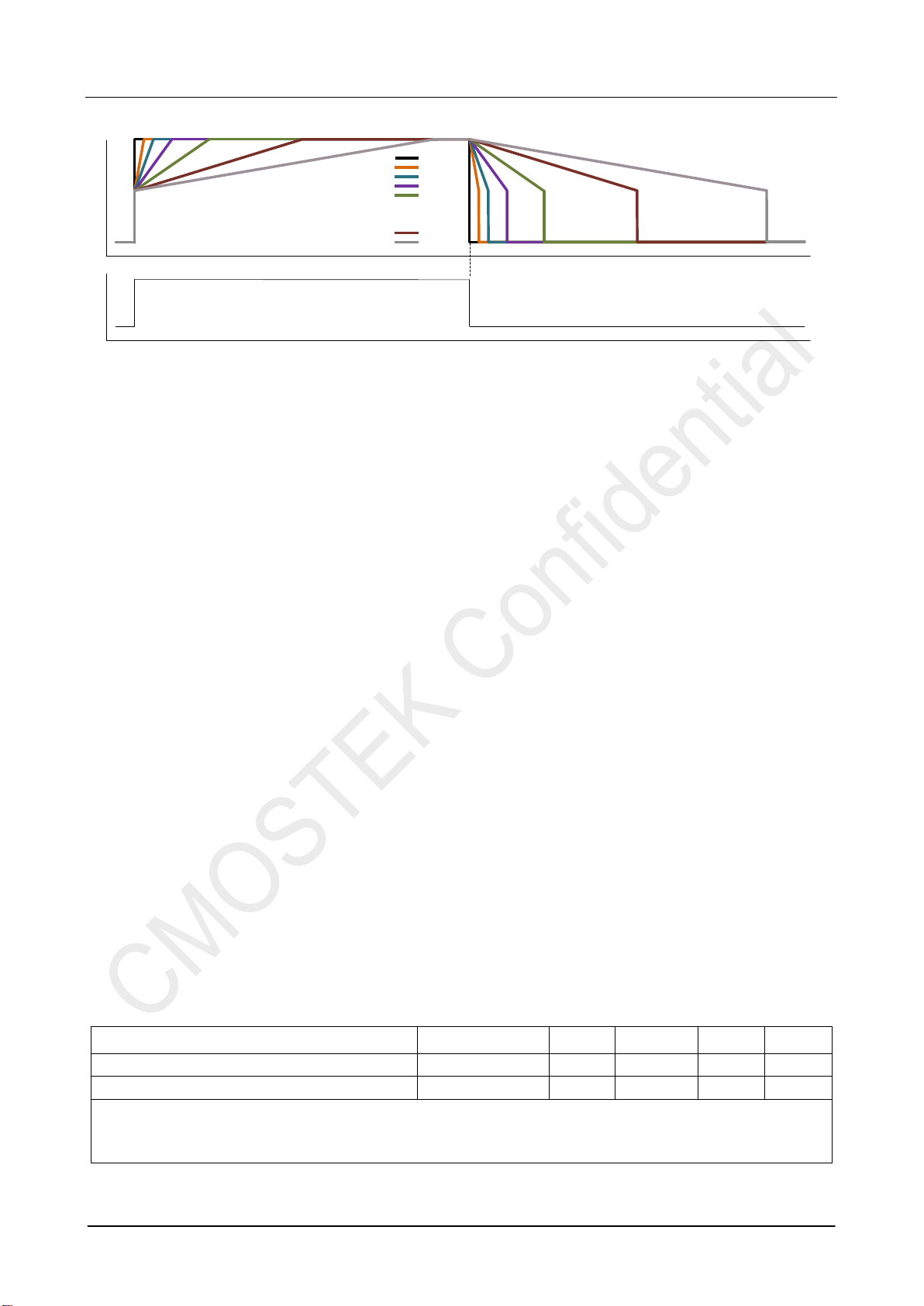
carrier frequency. By gradually ramping the PA on and off, PA transient spurs are minimized. The CMT2150A has built-in PA
ramping configurability with options of 0, 1, 2, 4, 8, 16, 32, 64, 128, 256, 512 and 1024 us, as shown in Figure 13. When the
option is set to “0”, the PA output power will ramp up to its configured value in the shortest possible time. The ramp down time
is identical to the ramp up time in the same configuration.
CMOSTEK recommends that the maximum symbol rate should be no higher than 1/2 of the PA ramping “rate”, as shown in the
formula below:
SR
Max
≤ 0.5 * ( 1
t
RAMP
)
In which the PA ramping “rate” is given by (1/tRAMP). In other words, by knowing the maximum symbol rate in the application,
the PA ramping time can be calculated by:
t
RAMP
≤ 0.5 * ( 1
SR
MAX
)
The user can select one of the values of the tRAMP in the available options that meet the above requirement. If somehow the
tRAMP is set to be longer than “0.5 * (1/SRMax)”, it will possibly bring additional challenges to the OOK demodulation of the Rx
device. For more detail of calculating tRAMP, please refer to “AN112 CMT2150A Configuration Guideline”.
CMT2150A
Rev 0.8 | Page 16/31
www.hoperf.com
Time
RFO Amplitude
Time
Data
Logic 1 Logic 0
1024 us
512 us
8 us
4 us
2 us
1 us
0 us
Figure 13. PA Ramping Time
5.6 Working States
The CMT2150A has following 4 different working states: SLEEP, XO-STARTUP, TUNE and TRANSMIT. The device stays in
the SLEEP state when no transmission is performed. Once the button(s) is/are pressed, the device goes through the sequence
of SLEEP XO-STARTUP TUNE TRANSMIT to transmit the data. After the transmission the device goes back to the
SLEEP state. When the device works in the periodic transmission mode, the device periodically wakes up from the SLEEP
state, goes the same sequence, performs the transmission and goes back to the SLEEP state. All the details of push button(s)
function and periodic transmission can be referred to “AN112 CMT2150A Configuration Guideline”.
SLEEP
When the CMT2150A is in the SLEEP state, all the internal blocks are turned off and the current consumption is minimized to
20 nA typically.
XO-STARTUP
Once the CMT2150A detects the valid button-pressing event, it will go into the XO-STARTUP state, and the internal XO starts
to work. The tXTAL is the time for the XO to get stable, it is to a large degree crystal dependent. Atypical value of tXTAL is
provided in the Table 11.
TUNE
The frequency synthesizer will tune the CMT2150A to the desired frequency in the time tTUNE. The PA can be turned on to
transmit the data generated by the embedded encoder only after the TUNE state is done.
TRANSMIT
The CMT2150A starts to modulate and transmit the data. The data packets being transmitted are generated by the embedded
encoder, and they are determined by the encoder selected, the button mode and the button being pressed.
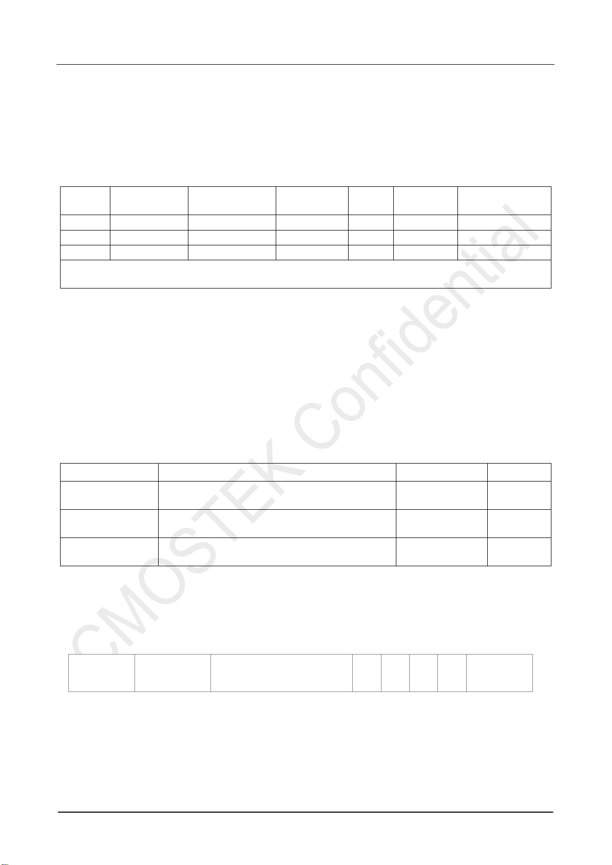
Table 11. Main Timing Spec in Different Working States
Parameter Symbol Min Typ Max Unit
XTAL Startup Time [1] tXTAL 400 us
Time to Tune to Desired Frequency[2] tTUNE
370
us
Notes:
[1]. This parameter is to a large degree crystal dependent.
[2]. From XO stable to ready to transmit.
CMT2150A
Rev 0.8 | Page 17/31
www.hoperf.com
5.7 The Encoder
The device supports 3 types of encoding formats: 1920, 1527 and 2262. The packets of these 3 modes have different
structures which will be introduced in below sub-sections. The table below summarizes the major features of the 3 encoding
formats.
Table 12. Feature Summary of the 3 Encoding Formats
Format Bit Format
(sym/bit) Sync ID Length
(bits) Data Length
(bits) CRC ID Study Button Modes[1]
1920 3/4/5/6 1 – 32 1 – 7 Support Support All
1527 4 20 1 – 7 NA Support All
2262 8 6 – 11 1 – 6 NA Not Support Normal Mode
Note:
[1]. Button Modes include Normal Mode, Matrix Mode, Toggle Mode and PWM Mode.
All the details of these 3 types of encoding formats are given in the document “AN112 CMT2150A Configuration Guideline”. The
following sections only give the abstracts of these formats. In the below explanations, some elements in the packet are measured
in the unit of “symbol”, while some of them are measured in the unit of “bit”. For those which have the unit of “bit”, one “bit” is
constructed (encoded) by several “symbols”. In the figures, “SYM” represents the word “symbol”.
5.7.1 1920 Packet Structure
Two types of packet structures are supported for 1920 format: Normal Packet and Study Packet. The following configurable
parameters are shared by the two structures.
Table 13. Configurable Parameters in 1920 Packet
Parameter Descriptions Default Mode
Preamble The size of the valid preamble, the options are: None or
16-symbol.
None Basic
Advanced
Address (Sync ID)
Length The range of the Sync ID Length is from 1 to 32 bits. 32-bit Basic
Advanced
Address (Sync ID)
Value The value of the Sync ID has the range from 0 to 2Length-1. 0 Basic
Advanced
Normal Packet
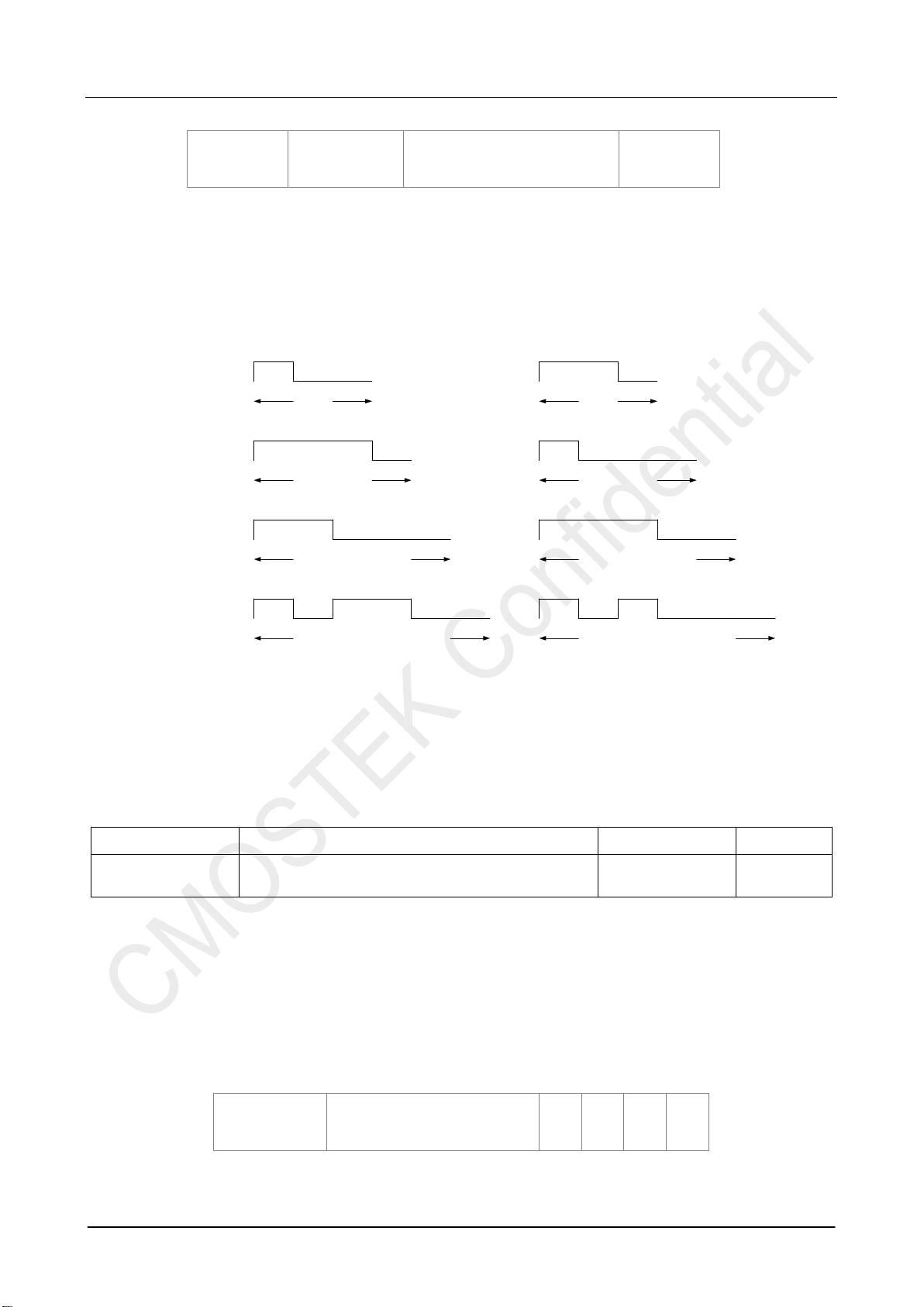
The normal packet is used to control the data pins of the CMOSTEK receiver CMT2250A or PWM output of the CMT2251A. It
contains a 16-symbol Preamble, a 32-symbol Head_N (which indicates that the current packet is a normal packet rather than a
study packet), a Sync ID, a Configurable Data Field and an 8-symbol CRC.
Preamble
16 symbols Address (Sync ID)
configurable 1-32 bits D0
1 bit D1
1 bit D2
1 bit D3
1 bit CRC
8 symbols
Head_N
32 symbols
Figure 14. 1920 Normal Packet Structure
Study Packet
The study packet is used for the CMT2250/51A to learn the Sync ID from the CMT2150A in order to pair the two devices. It
contains an optional Preamble, a 32-symbol Head_S, a Sync ID and an 8-symbol CRC.
CMT2150A
Rev 0.8 | Page 18/31
www.hoperf.com
Preamble
(Optional)
16-symbol
CRC
8-symbol
Head_S
32-symbol Address (Sync ID)
configurable 1-32 bits
Figure 15. 1920 Study Packet Structure
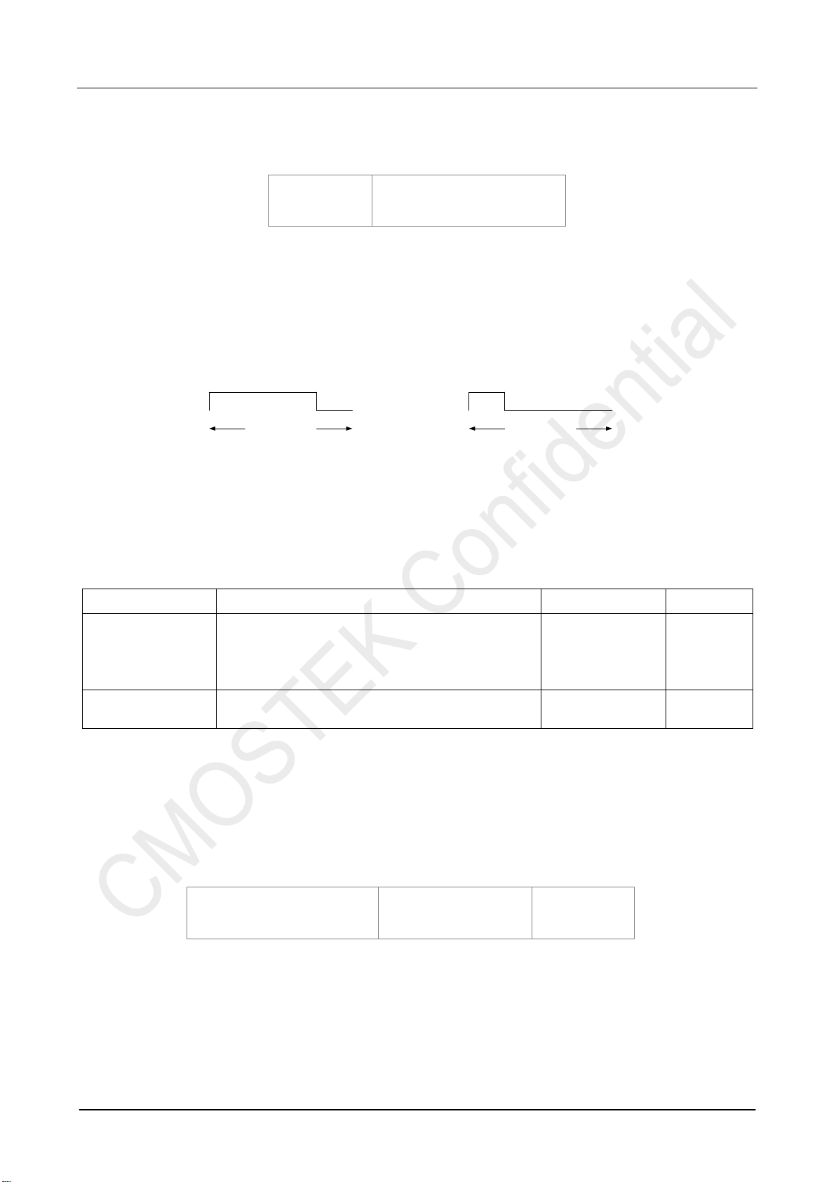
Bit Format
In 1920 packet, a single bit can be constructed (encoded) by 3, 4, 5 or 6 symbols. The user can select the desired value of the
“Bit Format” parameter on the RFPDK. Please note that only the Sync ID field and the D0, D1, D2, D3, D4, D5, D6 have the
unit of “bit”.
2 SYM2 SYM1 SYM 1 SYM
Bit 1 Bit 0
1 SYM1 SYM3 SYM 3 SYM
Bit 1 Bit 0
3 SYM2 SYM
Bit 1
2 SYM3 SYM
Bit 0
2 SYM1 SYM
Bit 1
1 SYM 2 SYM 1 SYM1 SYM
Bit 0
1 SYM 3 SYM
3 Symbols/Bit
4 Symbols/Bit
5 Symbols/Bit
6 Symbols/Bit
Figure 16. 1920 Bit Format Options
5.7.2 1527 Packet Structure
Two types of packet structures are supported for 1527 format: Normal Packet and Study Packet. The following configurable
parameter is shared by the two structures.
Table 14. Configurable Parameters in 1527 Packet
Parameter Descriptions Default Mode
Address (Sync ID)
Value The range of the Sync ID value is from 0 to 220-1. This is
because the Sync ID Length is fixed at 20 for 1527. 0 Basic
Advanced
In the traditional 1527 format, 8 OSC clocks are equal to 1 LCK, 4 LCK are equal to 1 symbol. By using the CMT2250A pairing
with CMT2150A, the user does not need to adjust the OSC to determine the symbol rate, because the symbol rate is directly
programmed. The Bit Format is fixed at 4 symbols (16 LCK) per bit.
Normal Packet
The traditional 1527 packet contains a 32-symbol Sync, a 20-bit Address (Sync ID) and 4-bit Data. CMOSTEK define a 1527
Study Packet to support the ID study in 1527 mode. The traditional packet introduced here is called the “Normal Packet”.
Address (Sync ID)
configurable 20 bits D0
1 bit D1
1 bit D2
1 bit D3
1 bit
Sync
32 symbols
Figure 17. 1527 Normal Packet Structure
CMT2150A
Rev 0.8 | Page 19/31
www.hoperf.com
Study Packet
The 1527 Study packet contains a 32-symbol Head_S and a 20-bit Address (Sync ID), as shown below.
Head_S
32-symbol Address (Sync ID)
20 bits
Figure 18. 1527 Study Packet Structure
Bit Format
In 1527 packet, a single bit is constructed by 4 symbols, as shown below. The user can select the desired value of the “Bit
Format” parameter on the RFPDK. Please note that only the Sync ID field and the D0, D1, D2, D3, D4, D5, D6 field have the
unit of “bit”.
1 SYM1 SYM3 SYM 3 SYM
Bit 1 Bit 0
Figure 19. 1527 Bit Format Options
5.7.3 2262 Packet Structure
ID Study is not supported in 2262 mode. Only one packet structure is supported.
Table 15. Configurable Parameters in 2262 Packet
Parameter Descriptions Default Mode
Address (Sync ID)
Length
This is the range of the Sync ID Length. The range is from
6 to 11 bits. This parameter also defines the number of
data bits, because the total number of Sync ID and Data
bits is fixed at 12.
8-bit Basic
Advanced
Address (Sync ID)
Value The value of each bit of the Sync ID can only be
represented by 0, 1 or f. 00000000 Basic
Advanced
In the traditional 2262 format, 4 OSC clocks (1 OSC clock cycle is notated as 1 α) are equal to 1 symbol. By using the
CMOSTEK products, the user does not need to adjust the OSC to define the symbol rate, because the symbol rate is directly
programmed. The Bit Format is fixed at 8 symbols per bit.
Normal Packet
The traditional 2262 packet contains an 8 to 11-bit Address (Sync ID), a 1 to 4-bit Data, and a 32-symbol Sync.
Address (Sync ID)
configurable 8-11 bits Data
4-1 bit(s) Sync
32 symbols
Figure 20. 2262 Packet Structure
Bit Format
In 2262 packet, a single bit is constructed by 8 symbols, as shown below. Please note that only the Address (Sync ID) field and
the Data field have the unit of “bit”. In the below diagram, 1 OSC clock cycle is notated as 1 α referring to the original 2262
timing descriptions.

CMT2150A
Rev 0.8 | Page 20/31
www.hoperf.com
3 SYM
(12 α)1 SYM
(4 α)3 SYM
(12 α)1 SYM
(4 α)
Bit 1
3 SYM
(12 α)
1 SYM
(4 α)
Bit 0
3 SYM
(12 α)
1 SYM
(4 α)
3 SYM
(12 α)1 SYM
(4 α)
Bit f
3 SYM
(12 α)
1 SYM
(4 α)
Figure 21. 2262 Bit Format Options
5.8 ID Study
The ID Study function, which is supported in 1920 and 1527 modes, allows the CMT2250/51A to receive the Sync ID sent by
the CMT2150A and burns it into the local EEPROM automatically. Since then, the CMT2250/51A’s Sync ID is identical to that
of the CMT2150A and therefore two devices are paired. The lengths of the Sync ID are different in the different packet formats.
In 1920 format, it is from 1 to 32 bits. In 1527 format, it is fixed at 20 bits.
The ID Study is initialized by the CMT2150A. It is done by executing the following steps:
1. Press the Study Button on the CMT2150A and hold it over the time defined by the “Study Trigger Time”.
2. CMT2150A starts to transmit the Study Packets, wait 1-2 seconds then release the Study Button.
3. Try to press a certain button on the CMT2150A to check if the CMT2250/51A react correctly.
The figure below shows the timing characteristic after pressing down a study button. The Study Power is always independently
configured from the TX Power. In this example, the Study Power is set smaller than the TX Power.
One Normal
Packet Packet
Interval
Study Button
Pressed
time
Study Button
Released
Study Time
(Default is 5 s)
One Study
Packet Packet
Interval
TX Power = 0 dBm Study Power = -6 dBm
Figure 22. Timing of Study Button Pressing Event
More information about the ID Study can be found in the document “AN112 CMT2150A Configuration Guideline”.
5.9 Button Modes
The button modes define the functions of the input pins K1 – K7. The CMT2150A supports 4 different button modes: Normal,
Matrix, Toggle and PWM, which are configured on the RFPDK. The following sections give the abstract of each button mode.
All the details of the button modes are given in the document “AN112 CMT2150A Configuration Guideline”.
5.9.1 Normal
The Normal Button Mode is supported in 1920, 1527 and 2262 format. In this mode, the buttons are directly mapped to the
data field of the packet. Multiple buttons can be pressed at the same time. For 1920 and 1527, the largest number of buttons is
7 which are defined by the parameter “Number of Button(s)”. For 2262, the largest number of buttons is 6, which is determined
by the Sync ID Length. The figure below gives an example which 4 push button keys are selected.
Other manuals for CMT2150A
1
This manual suits for next models
2
Table of contents
Other CMOSTEK Transmitter manuals
Popular Transmitter manuals by other brands

Vega
Vega VEGABAR 82 operating instructions

Hyundai
Hyundai H-FMT11 instruction manual

Mil-Ram Technology, Inc.
Mil-Ram Technology, Inc. TA-2102 instruction manual
Cypress
Cypress CA-COMPAT Operation manual
Superior Broadcast
Superior Broadcast SBFM100-SS user manual

ATX
ATX QFOT1L Installation & operation manual
