CMOSTEK CMT21 Series Guide

AN121
Rev 0.6 | 1/12
www.cmostek.com
Overview
When the CMT21xx series chips provided by CMOSTEK are used under the conditions of direct human body contact, especially
in handheld devices, the ESD differs according to different places and seasons. This document aims for providing guidelines for
users to improve chip anti-ESD capabilities mainly from the aspects of handheld device structure design and PCB design hence
to improve the product anti-ESD capability.
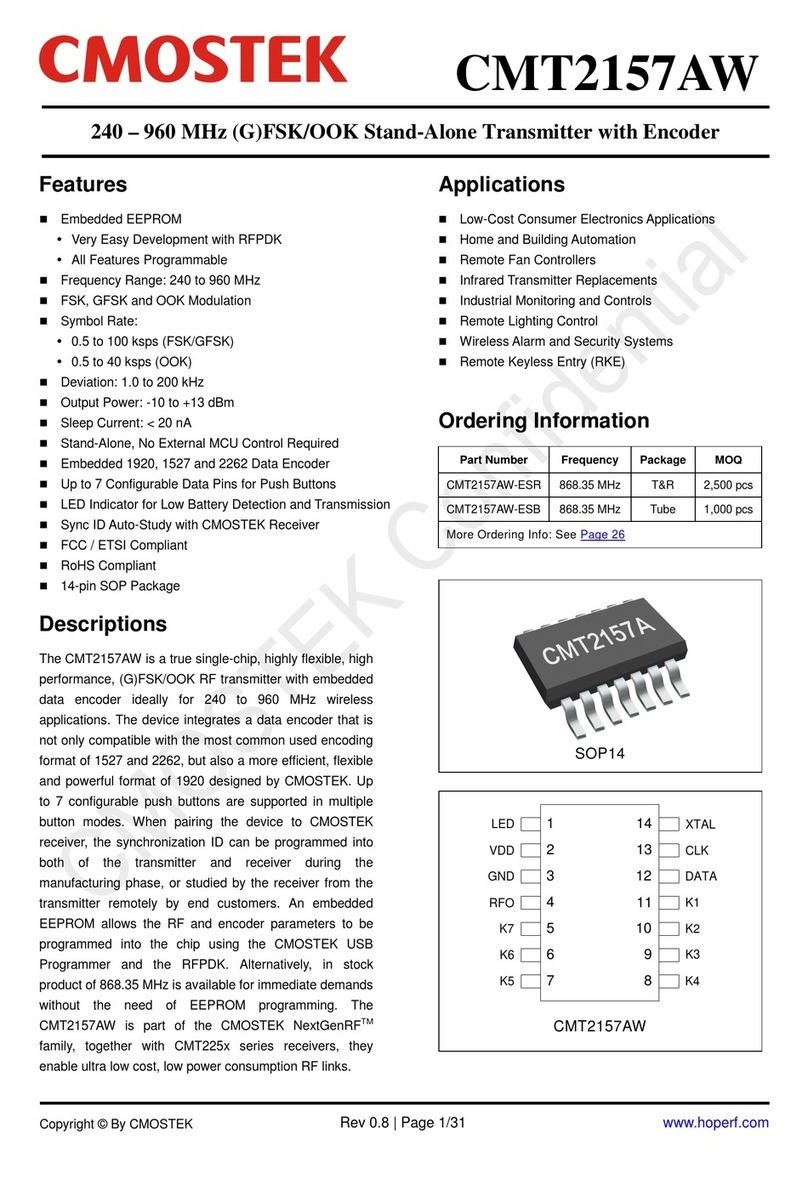
The product models covered in this document are shown in the table below.
Table 1. Product Models Covered in This Document
Product
Model
Frequency
(MHz)
Modulation
Method
Chip Function
Configuration
Method
Package
CMT2150A
240-480 MHz
OOK
7- key transmitter with encoder
EEPROM
SOP14
CMT2157A
240-960 MHz
(G)FSK/OOK
7- key transmitter with encoder
EEPROM
SOP14
CMT2180A
240-480 MHz
OOK
Transmitter Soc
EEPROM / Flash
SOP14
CMT2189A
240-960 MHz
(G)FSK/OOK
Transmitter Soc
EEPROM / Flash
SOP14
CMT2110A
240-480 MHz
OOK
Single-wire, direct mode, transmitter-only
EEPROM
SOT23-6
CMT2119A
240-960 MHz
(G)FSK/OOK
Single-wire, direct mode, transmitter-only
EEPROM/Registers
SOT23-6
This document will discuss the ESD protection per CMT21xx chips used in handheld devices from the following perspectives.
causes and harms
anti-ESD design
AN121
CMT21xx Handheld Device Design Guide
Copyright ©By CMOSTEK

AN121
Rev 0.6 | 2/12
www.cmostek.com
Table of Contents
1ESD Causes and Harms................................................................................................................... 3
2ESD Transmission Route................................................................................................................. 4
3ESD Protection & Anti-interference Design................................................................................... 5
3.1 Improve Anti-ESD Capability in Structure Design...............................................................................................5
3.2 PCB Anti-ESD Design........................................................................................................................................ 7
4Revise History..................................................................................................................................11
5Contacts........................................................................................................................................... 12

AN121
Rev 0.6 | 3/12
www.cmostek.com
1 ESD Causes and Harms
Causes of static electricity mainly includes friction, peeling and induction.
Figure 1. Main Causes of ESD Occurring
Under different humidity, the ESD cuased by various human body activities is different.
Table 2. Correlation between ESD Derived from Various Human Activity and Humidity
Human Body Activity
Humidity 10-20%(V)
Humidity 65-90%(V)
Walking on chemical fiber floor cover
35,000
1,500
Taking a TEFLON wafer holder
30,000
1,200
Walking on chemical fiber floor
12,000
250
Working while sitting on a chair
6,000
100
Flipping a plastic sealed instruction book
7,000
600
Picking up a polyethylene bag
20,000
1,000
Sitting on a polyester foam pad
18,000
1,500
ESD can be generated even in a 99% humidity environment. The human body responses to ESD electrostatic voltages are as
follows (IEC 61000-4-2, human body model).
Table 3. Human Body Response to ESD Electrostatic Voltage
Electrostatic Voltage(V)
Human Body Response
1,000
Human body does not feel
2,000
Outside of fingers can feel
2,500
The discharging part can feel slight sharp-pain.
3,000
Can feel slight and moderate sharp-pain.
4,000
Fingers feel slight pain and strong sharp-pain.
5,000
Palm and wrist feel strong electric-shock.
6,000
Fingers feel very severe pain and the back of wrist feels strong electric-shock.
10,000
The whole wrist feels strong pain and the body feels current passing through.
12,000
Due to strong electric shock, the entire hand has a sense of heavy blow
Friction
Peeling
Induction

AN121
Rev 0.6 | 4/12
www.cmostek.com
2 ESD Transmission Route
For handheld devices, there exists potential difference between human bodies and handheld devices. As long as a potential
difference exists, there's a strong electric field established. Once the voltage exceeds the breakdown voltage between the air and
the insulating medium, an arc will be generated and it will keep until the conditions producing it disappear.
Figure 2. ESD of Handheld Devices
ESD can be introduced into handheld devices through 5 coupling paths as below.
1. The initial electric field energy can have capacitive couple with the trace networks which have a relatively large surface
area.
2. Charge/current is injected directly through the arc.
3. The current can cause voltage pulses (V = L ×dI / dt) on the conductors such as power, ground and signal traces. The
current pulses will enter each common element connected in these networks.
4. The arc will produce a strong magnetic field with a frequency range of 1 MHz to 500 MHz and is inductively coupled to each
adjacent trace loop.
5. The electromagnetic field radiated by the arc will be coupled to long signal traces acting as receiving antennas.
ESD will catch the weak points of handheld devices through a variety of coupling paths. To avoid interference and damage from
ESD events, users should isolate these coupling paths or strengthen the anti-ESD capability accordingly.

AN121
Rev 0.6 | 5/12
www.cmostek.com
3 ESD Protection & Anti-interference Design
3.1 Improve Anti-ESD Capability in Structure Design
CMOSTEK's NextGenRFTM series products are high-performance, highly integrated CMOS devices, which
are relatively subject to ESD impact like device breakdown, which may result in malfunction or direct damage
to the devices. Hence, users should take ESD protection into careful consideration in both product design
and production.
For most of the CMT21xx series chip products which are used in handheld devices, applying proper isolation is the key. In
general, a plastic casing is used to seal the internal electronic circuits as the non-conductor plastic casing can block the ESD arc
discharge coupling effectively. A button panel is usually isolated by a silicone panel. It should be noted that the isolation effect
varies from different sealing conditions of joint gaps and interface gaps and the distance between the edge of the internal
electronic circuit and the edge of the casing.
The devices should meet the following ESD isolation requirements.
1. Avoid to use conductive parts such as metal on the surface of a casing or in a gap . When such components are used, the
space between the components and the internal trace should be insulated again for separation.
Figure 3. Changing a Metal Part to a Non-metal Part
2. Gap sealing conditions: the smaller the gap, the better. If it is not sufficient, place ESD-absorbing soft silicone pad or
high-impedance insulating material in the gap.
Figure 4. Ensure Gaps Sealed Well
The gap near the
casing is isolated by
paper

AN121
Rev 0.6 | 6/12
www.cmostek.com
3. When metal parts from the outer casing is inserted, put silicone pads and place antistatic glue for isolation.
Figure 5. Isolate Static Path of Inserted Metal
4. To prevent the secondary arc from striking the internal electronic circuit, keep a certain distance between the internal PCB
and either the surfaces of metal parts or the gaps. The long the distance, the better. Keep a 3 mm distance at least.
Figure 6. Keep Distance between Internal Circuit and Edge of Structure
5. At the end of outside electrical connections, the input, output, and power traces need to be protected. For example, a
voltage transient suppressor (electrostatic protection diode, etc.) is placed between the power supply and the ground. In
general, a common interface has a ground connecting to the internal ground trace. These two ground traces should not be
connected directly. It is recommended to add a 0 Ω resistor or a low-resistance magnetic bead at the connection end, and
add sawtooth discharge and copper plane between the two ground traces to reduce direct ESD damage as shown in the
below figure.
加硅胶片、高阻抗
纸片、硅胶隔离
金属与板边的
距离大于3mm
Place silicone sheet, high-impedance
paper and silicone for isolation
Keep the distance between the metal and the
board edge larger than 3 mm for isolation.

AN121
Rev 0.6 | 7/12
www.cmostek.com
Figure 7. ESD Protection of External Circuit Interface
Whenever possible, use enough shield, such as iron frame, copper foil, etc., to protect the electronic circuit, , and keep a safe
distance between the component and the shield. The shield should have good contact with the main ground and is placed as far
away as possible from ESD sources.
Figure 8. Use Shield to Protect Electronic Circuit
3.2 PCB Anti-ESD Design
Proper PCB layout can improve the anti-ESD capability of sensitive components then to fulfill the PCB anti-ESD design.
1. Use multi-layer PCB design as much as possible, which can help improve product anti-ESD capability.
2. Place power trace close to ground trace. Make signal traces as short as possible and place them close to ground to reduce
the loop area. Try to avoid place sensitive signals such as /RESET close to the edge of the board. Try to wrap all traces
within ground traces.
D1
D2
Vdd
Vp
ESD
输入端
Vn
ESD 保
护元件
IESD
ESD
Protection
Component
s
ESD input end

AN121
Rev 0.6 | 8/12
www.cmostek.com
Figure 9. Wrap All Traces within Ground Traces
3. Try to make the circuit design compact. Place sensitive components away from ESD sources. Leave only ground loop trace
around the edge of the board. The width of ground loop trace should be more than 3.5 mm and hollow ground loops should
be avoided.
4. Fill the unused area with ground and connect the grounds of both sides with vias at every a certain distance (less than 5
mm). The wider the ground trace, the smaller the connection resistance, the better. The grounds of both the main board and
the whole system should be integrated altogether, namely, avoid to separate them. However, the separation of trace layer is
inevitable. According to this, more vias should be placed to connect the trace layer with the below ground, which helps
improve anti-ESD capability.
Figure 10. Fill Empty Area with Ground
5. ESD can be absorbed by point discharge easily. Place sharp conductors at places where it can be shielded to absorb ESD.
However , in sensitive areas, sharp conductor wires should be reduced and insulator cover should be used instead along
with shield layer wrap.
6. At signal input ends connecting to outside, and power supply ends, it is easy to introduce ESD discharge. Therefore,
enti-ESD components should be placed between signal traces near interface end and ground and between power supply
traces and ground. Users should take careful consideration in where to place anti-ESD component. The anti-ESD
components should be placed as close as possible to electrostatic induction ports but away from the protected
components.
Wrap all traces
within ground
traces
Fill empty
area with
ground and
place more
vias there

AN121
Rev 0.6 | 9/12
www.cmostek.com
Figure 11. Use ESD Protection Components to Have Protection
7. Ground traces should be placed as large as possible, and try to connect ESD with the shortest trace distance, namely, the
ground area of the product should be as large as possible and make the ground trace distance as short as possible.
Figure 12. Place Large Ground Trace
8. Try to use round traces overall to improve anti-ESD capability.
Figure 13. Try to Arrange Round Traces Overall
ESD
Sensitive
Components
Shield ground
Signal ground
Try to arrange
round traces
overall

AN121
Rev 0.6 | 10/12
www.cmostek.com
9. LOOP antennas should not be placed too close to the edge of the board, namely, keep a space of 0.3 mm at least.
Meanwhile, ESD should be relieved to the ground with a resistor or TVS tube (it depends on users' outer casing design and
the ESD rating requirements).
Figure 14.Keep a Space between LOOP Antenna and Board Edge
10. Add a resistor to traces which are easy to introduce ESD, which helps to improve the anti-ESD capability.
Figure 15. Add Resistors on Traces for ESD Protection
11. Add a TVS tube between power supply and ground to discharge ESD (it depends on users' outer casing design and the
ESD rating requirements).
12. If a 49US crystal is used, better connect it to ground. Note that the 3225 crystal has better anti-ESD performance than that
of the 49US crystal .
Keep a space of at
least 0.3 mm
between LOOP
antenna and board
edge
Add resistors

AN121
Rev 0.6 | 11/12
www.cmostek.com
4 Revise History
Table 4. Revise History Records
Version No.
Chapter
Description
Date
0.6
All
Initial version
2016-2-17

AN121
Rev 0.6 | 12/12
www.cmostek.com
5 Contacts
CMOSTEK Microelectronics Co., Ltd. Shenzhen Branch
Address: 2/F Building 3, Pingshan Private Enterprise S.T. Park, Xili, Nanshan District, Shenzhen, Guangdong, China
Tel: +86-755-83231427
Post Code: 518071
Sales: sales@cmostek.com
Supports: sup[email protected]
Website: www.cmostek.com
The information furnished by CMOSTEK is believed to be accurate and reliable. However, no responsibility is assumed for
inaccuracies and specifications within this document are subject to change without notice. The material contained herein is
the exclusive property of CMOSTEK and shall not be distributed, reproduced, or disclosed in whole or in part without prior
written permission of CMOSTEK. CMOSTEK products are not authorized for use as critical components in life support
devices or systems without express written approval of CMOSTEK. The CMOSTEK logo is a registered trademark of
CMOSTEK Microelectronics Co., Ltd. All other names are the property of their respective owners.
Copyright. CMOSTEK Microelectronics Co., Ltd. All rights are reserved.
This manual suits for next models
6
Table of contents
Other CMOSTEK Transmitter manuals
Popular Transmitter manuals by other brands
Black Box
Black Box FiberPath AC444A Specifications

Blu Stream
Blu Stream HEX31WPB-TX user manual
Orange RX
Orange RX TX6i instruction manual
I.SOUND
I.SOUND WIRELESS FM TRANSMITTER datasheet

DGFLOW
DGFLOW TEEVALVE 10 1 1/2 Operator and maintenance manual
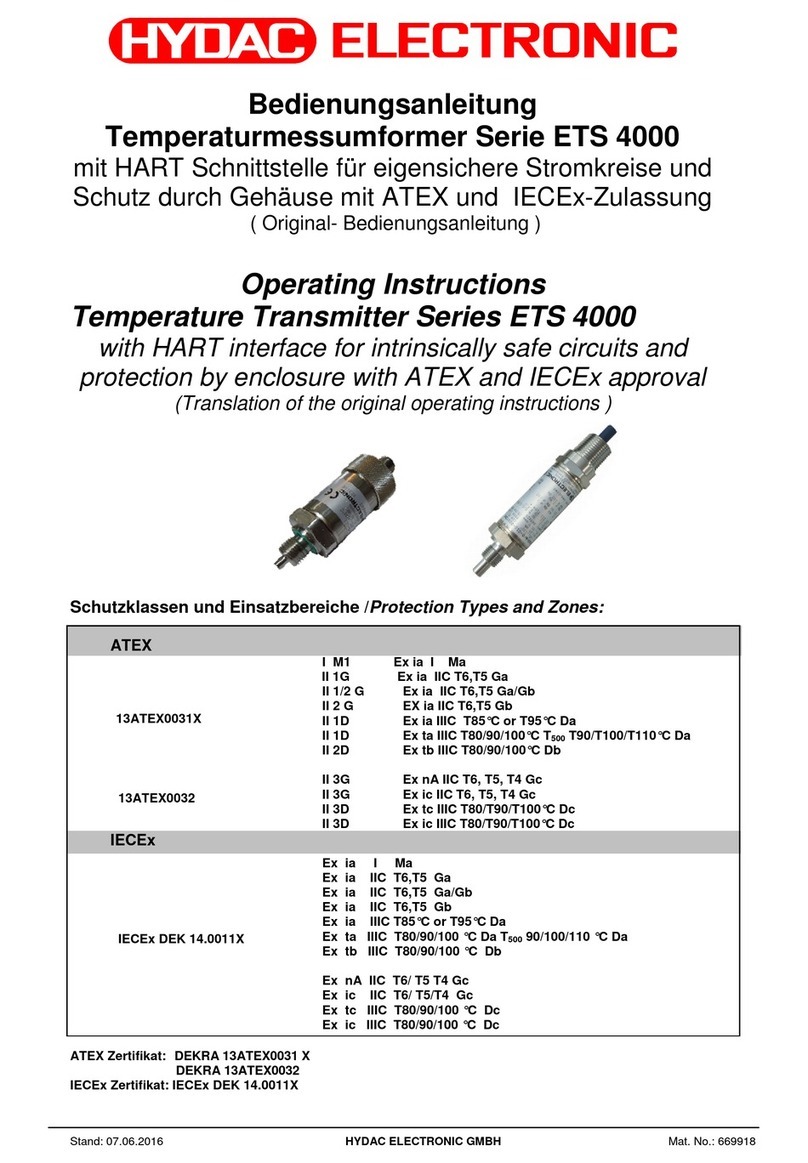
HYDACELECTRONIC
HYDACELECTRONIC ETS 4000 Series operating instructions
