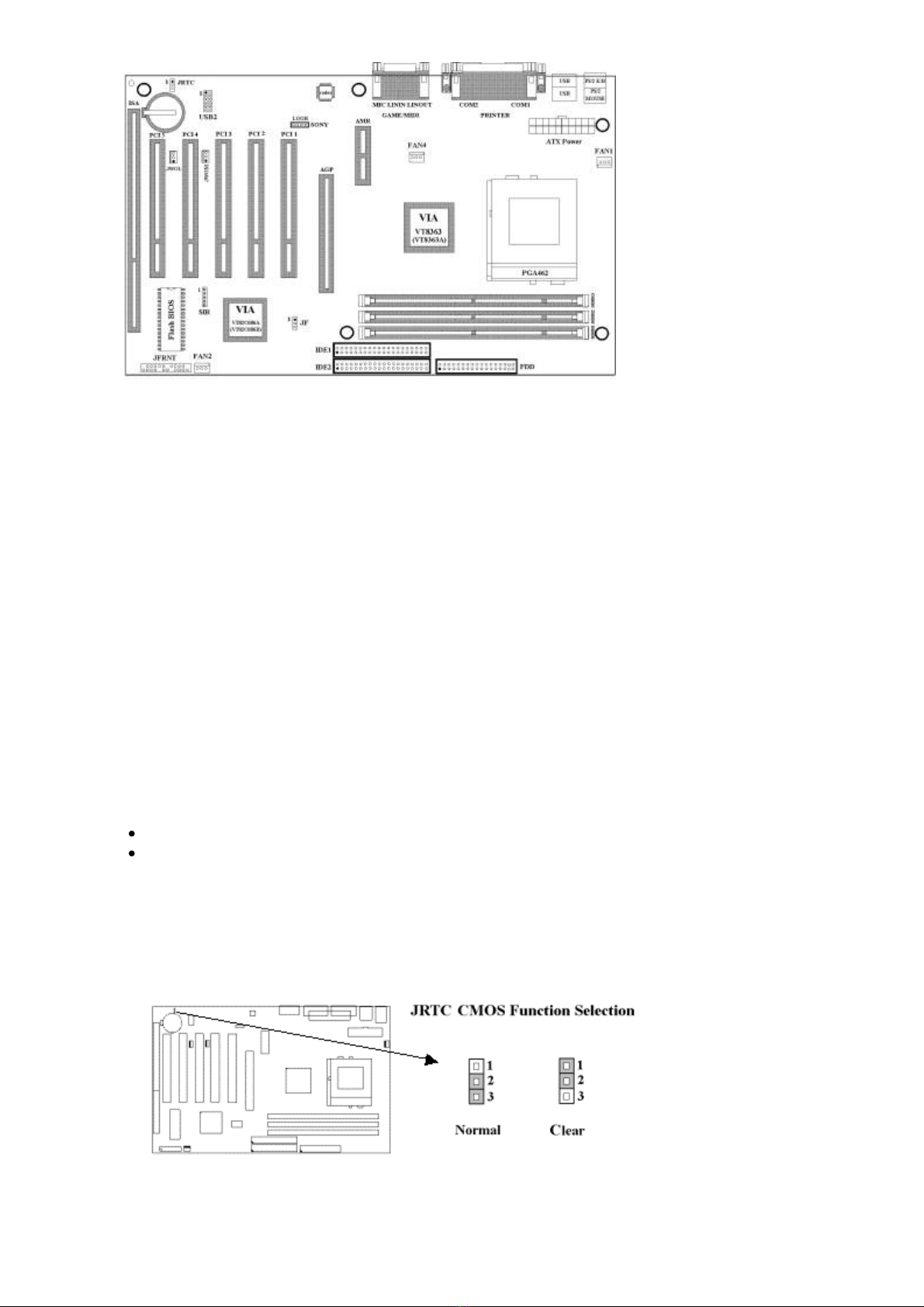
2.2 Installation of CPU
Before installing CPU, make sure the power is off. Locate the level bar on the PGA462 ZIF socket. Push level bar
away from the socket and pull upward 90 degrees. Insert the CPU into the socket. Be careful of CPU orientation.
Make sure the notch of the CPU corresponds with the white dot on the ZIF socket (the corner without pin socket). Do
not push in the CPU. Make sure all pins are aligned with the CPU socket. ON the level bar.
2.3 Installation of Memory
The motherboard has 3x168-pin 64-bit Dual Inline Memory Module (DIMM) sockets divided into 3 banks.
You can install 3.3V Unbuffered PC100/133-compliant Synchronous DRAM (SDRAM) memory. This will
increase the system reliability.
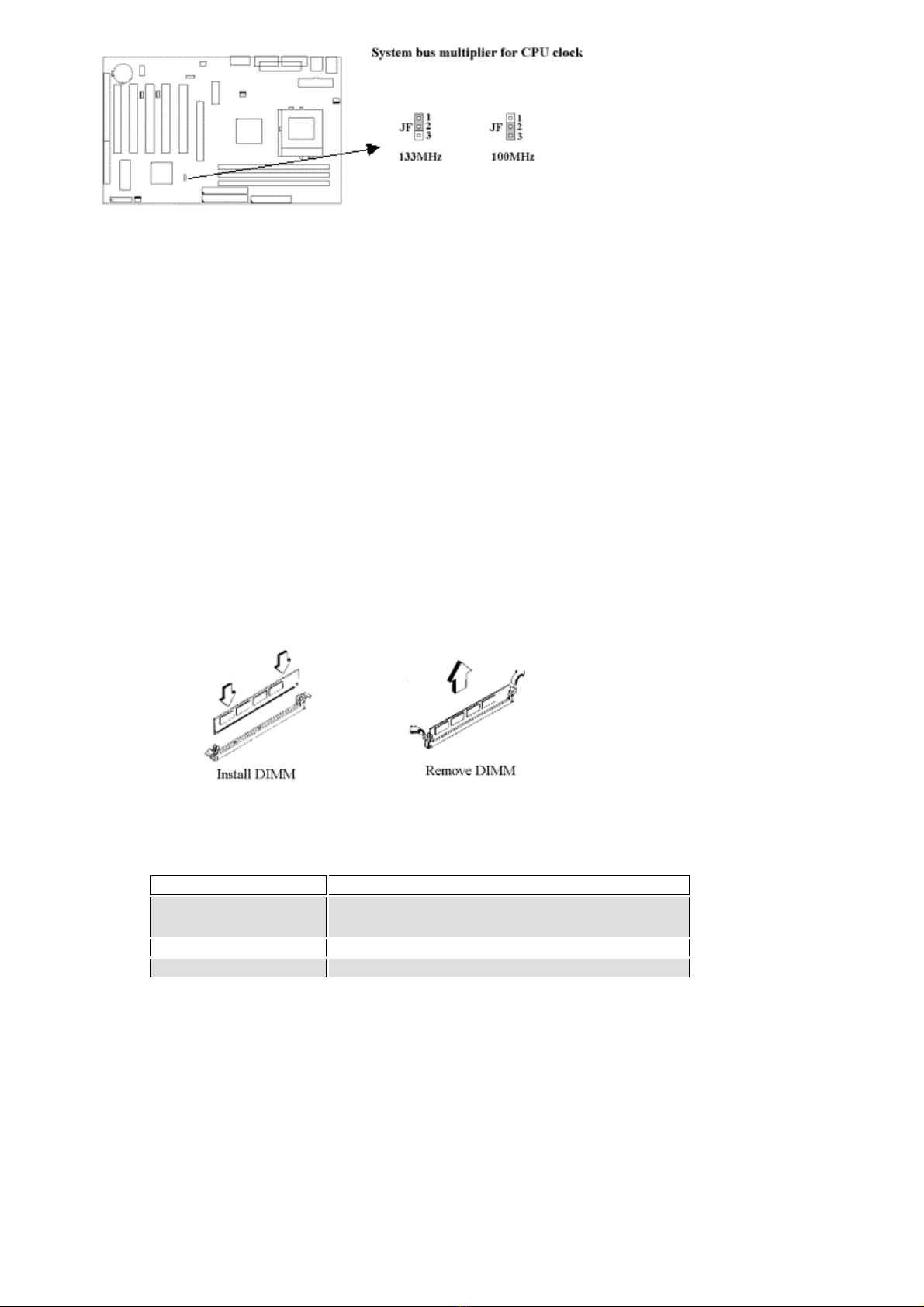
2.3.1 Installation of 168-pin DIMM (Dual Inline Memory Module)
1. Before inserting the DIMM, make sure the pin1 of the DIMM matches with the pin1 on the
DIMM socket.
2. Insert DIMM into the DIMM sockets at a 90-degree angle and press down.
2.3.2 Removal of 168-pin DIMM
Press the holding clips on both sides of the socket outward to release the DIMM.
Gently pull the DIMM out of the socket.
2.3.3 Memory Configuration
There is no jumper setting required for the memory size or type. It is automatically detected by the
system BIOS, and the total memory size is to add them together.
DIMM Socket DIMM Modules
DIMM1 PC100/PC133, 8, 16, 32, 64, 128, 256, 512MB
IMM2 PC100/PC133, 8, 16, 32, 64, 128, 256, 512MB
DIMM3 PC100/PC133, 8, 16, 32, 64, 128, 256, 512MB
2.4 I/O Connections/Panel Connections
I/O Connections
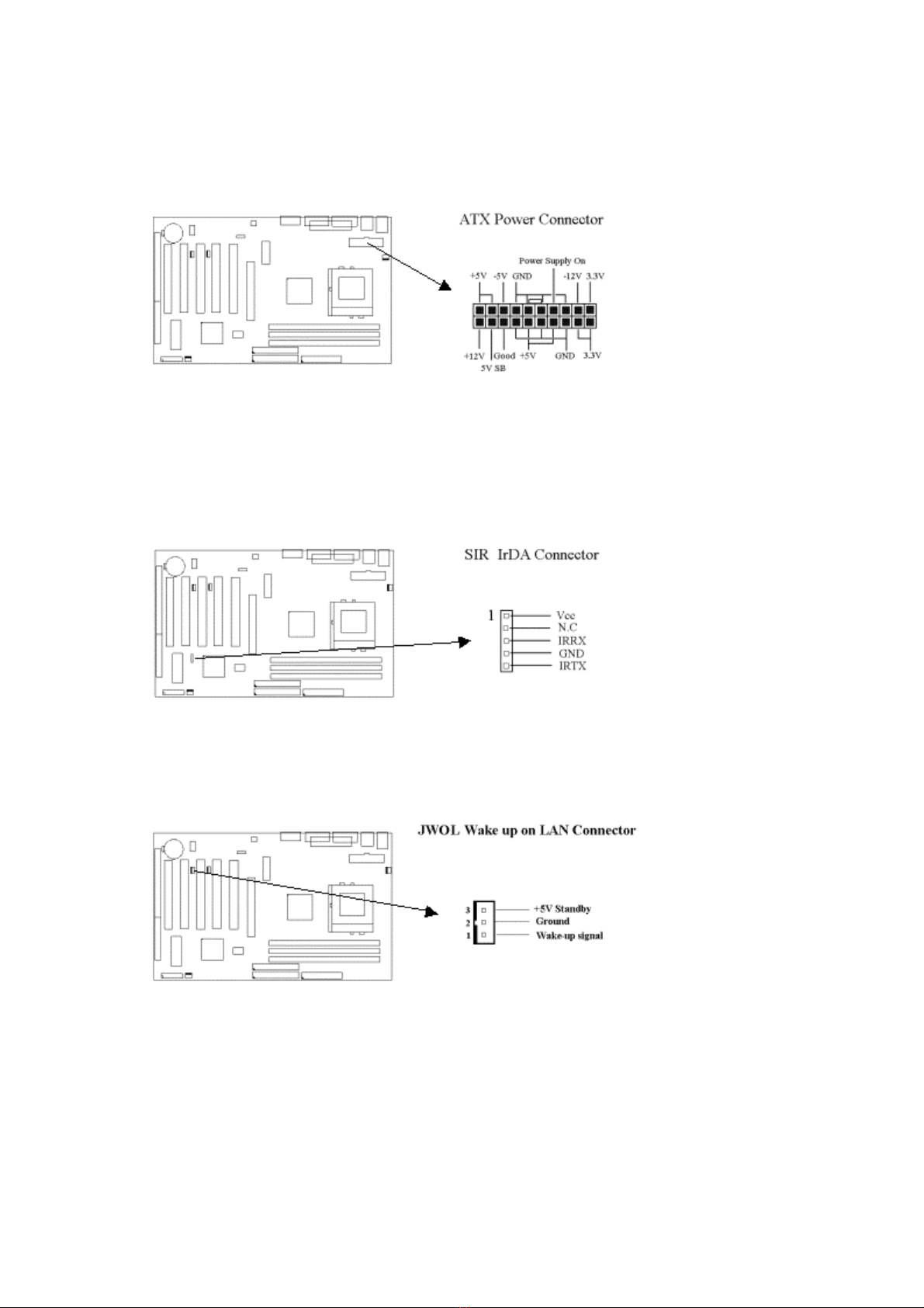
ATXPWR ATX Power Connector
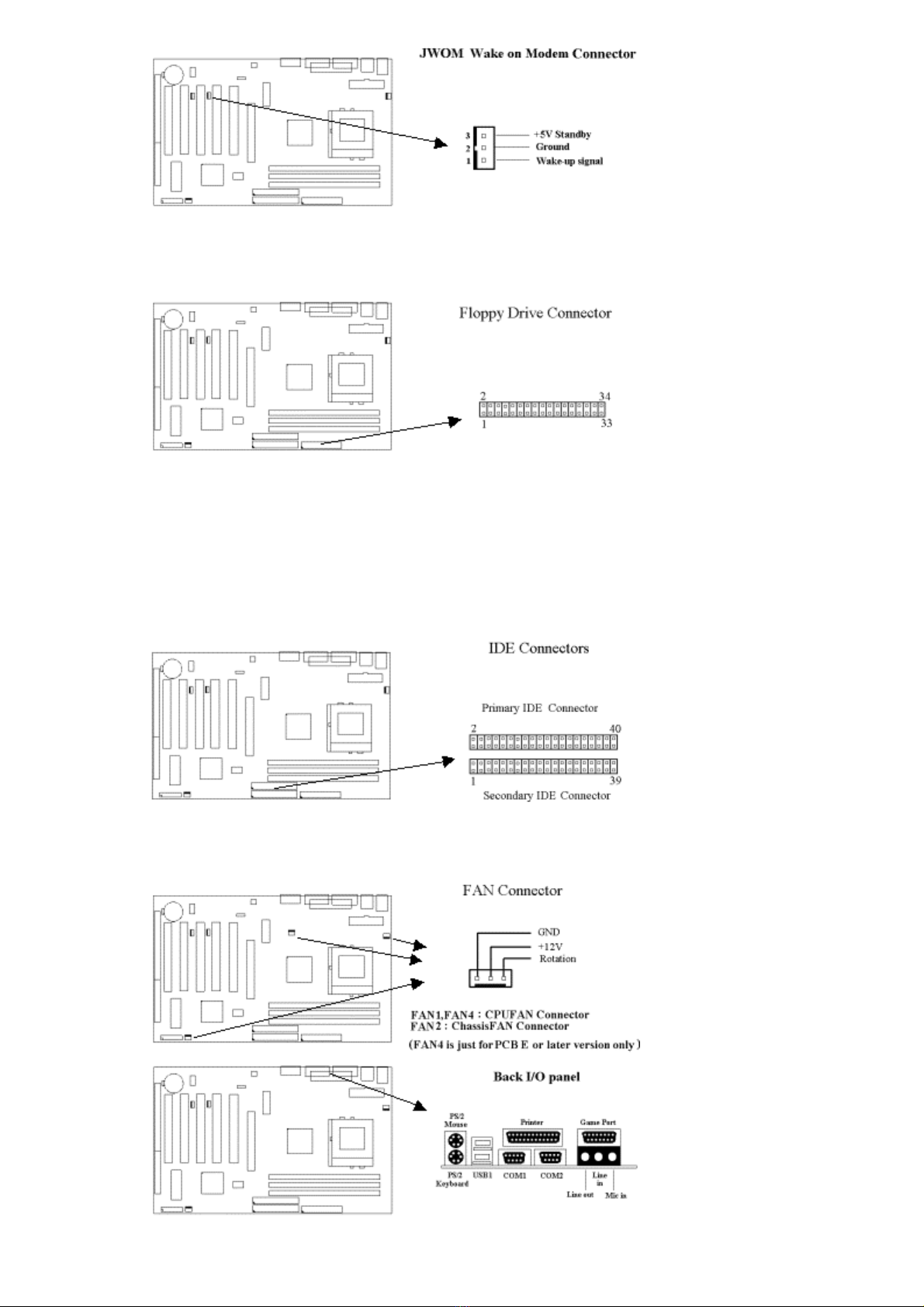
FAN1, 4 CPU fan connector (FAN4 is just for PCB E or later version only)
FAN2 Chassis fan connector
SIR Infrared Connector ( Cable optional )
JWOL Wake up on LAN connector
JWOM Wake up on Modem connector
FDD Floppy Disk Drive Connector
IDE1, 2 Primary/ Secondary IDE Connectors
CN1 PS/2 Mouse Port & Keyboard Connector
COM1, 2 Serial Ports 1 & 2
PRINTER Printer Port
USB1, 2 USB Connector ( Cable optional )