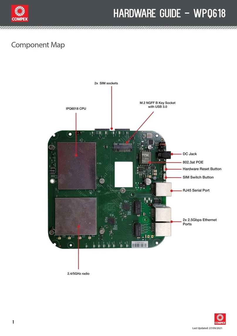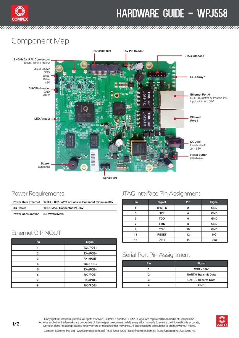
hardware guide - wpq865 6B02
2
Compex
Systems
Pte
Ltd
|
www
.compex.com.sg
|
(+65)
6288
8220
|
[email protected] |
Last
Updated:
08/02/2018
WH
XG
KG
Copyright © Compex Systems. All rights reserved. COMPEX and the COMPEX logo, are registered trademarks of Compex Inc.
Atheros and other trademarks are properties of their respective owners. While every effort is made to ensure the information is accurate,
Compex does not accept liability for any errors or mistakes that may arise. All specifications are subject to change without notice.
Power Requirements
Power Over Ethernet 1x IEEE 802.3af/at POE, 36~57V, up to 70W (4-pair
power feed) on WAN Port
DC Power 1x DC Jack Connector: 12V, 4A
Power Consumption 4.5W (board only)
SIM Slot Pin Assignment
SIM
Pin SIM1 SIM2 SIM Signal
1 C1 VCC VCC
2 C2 RST SIM_RST
3 C3 CLK SIM_CLK
4 C4 CD SIM_CARD_IN
5 C5 GND GND
6 C6 VPP VPP
7 C7 I/O SIM_DATA
e-SIM
Pin SIM3 SIM4 SIM Signal
1 C5 GND GND
2 C6 VPP UIM_VPP
3 C7 I/O SIM2_I/O
5 C4 NC NC
6 C3 CLK SIM2_CLK
7 C2 RST SIM2_RST
8 C1 VCC VCC
LED Pin Mapping
LED Indicators
DS22 ETH_LED4 DS11 POWER
DS4 ETH_LED3 LED1 LED_WLAN_L (for slot1)
DS3 ETH_LED2 LED2 LED_WLAN_L (for slot2)
DS1 ETH_LED1 LED10 LED_WLAN_L (for slot3)
DS2 ETH_LED0
WAN/PoE Pin Assignment
Pin Signal
1 TX+/POE+
2 TX-/POE+
3 RX+/POE-
4 TX+/POE+
5 TX-/POE+
6 RX-/POE-
7 RX+/POE-
8 RX-/POE-
FW Boot Cong Flash
Signal Config Jumper Location
BOOT_CONFIG2 NAND Flash JP13
BOOT_CONFIG0 NOR Flash JP9
Serial Port Pin Assignment
Serial Port from Pin Header
J23 Pin Signal
1 VCC – 3.3V
2 UART Transmit Data
3 UART Receive Data
4 GND
miniPCIe Slot 1 (J9, 4.0mm height)
Pin Assignment
Top side Bottom side
1 WAKE_L 2 +3.3V
3 NC 4 GND
5 NC 6 NC
7 CLKREQ_L 8 NC
9 GND 10 NC
11 REFCLK- 12 NC
13 REFCLK+ 14 NC
15 GND 16 NC
Mechanical key
17 NC 18 GND
19 NC 20 NC
21 GND 22 PERST_L
23 PERX_N 24 +3.3V
25 PERX_P 26 GND
27 GND 28 NC
29 GND 30 NC
31 PETX_N 32 NC
33 PETX_P 34 GND
35 GND 36 NC
37 NC 38 NC
39 +3.3V 40 GND
41 +3.3V 42 NC
43 NC 44 LED_WLAN_L
45 +5V 46 NC
47 +5V 48 NC
49 +5V 50 GND
51 +5V 52 +3.3V


