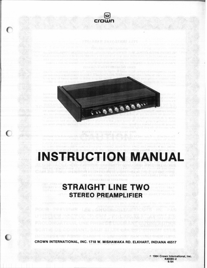
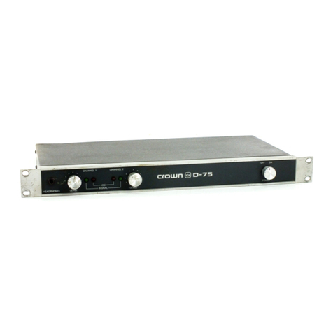
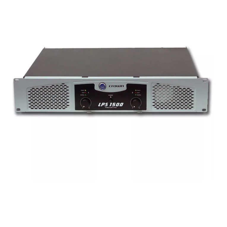
Crown K1 User manual

Service Manual
KSVCK1K2
03/98
Rev. A
K SERIESK SERIES
K SERIESK SERIES
K SERIES
PROFESSIONAL AUDIO AMPLIFIERSPROFESSIONAL AUDIO AMPLIFIERS
PROFESSIONAL AUDIO AMPLIFIERS
Models:
K1, K2
© 1999 by Crown International, Inc., P.O. Box 1000, Elkhart, Indiana 46515-1000 U.S.A. Telephone: 219-
294-8000.
K Series
amplifiers are produced by Crown International, Inc. Trademark Notice:
Balanced
Current Amplifier
™ is a trademark, and
Crown®
and
BCA®
are registered trademarks of Crown
International, Inc. Other trademarks are the property of their respective owners.
BALANCED CURRENT AMPLIFIER
Enable
Clip
Thermal
Signal
IOC
2
Enable
Clip
Thermal
Signal
IOC
2
1
0dB
3
1
5
7
9
11
13
15
17
19
21
25
45
30
100
1
1
0dB
3
1
5
7
9
11
13
15
17
19
21
25
45
30
100
1
0dB
3
1
5
7
9
11
13
15
17
19
21
25
45
30
100
0dB
3
1
5
7
9
11
13
15
17
19
21
25
45
30
100

K Series Service Manual
Rev. A
©1999 Crown International, Inc.
The information furnished in this manual does not include all of the details of design, production, or variations
of the equipment. Nor does it cover every possible situation which may arise during installation, operation or
maintenance. If you need special assistance beyond the scope of this manual, please contact the Crown
Technical Support Group.
Mail:
P.O. Box 1000 Elkhart IN 46515-1000
Shipping:
Plant 2 S.W., 1718 W. Mishawaka Rd., Elkhart IN 46517
Phone:
(800) 342-6939/(219) 294-8200
FAX:
(219) 294-8301
Web
: www.crownaudio.com
À PRÉVENIR LE CHOC
ÉLECTRIQUE N’ENLEVEZ
PAS LES COUVERTURES.
RIEN DES PARTIES
UTILES À L’INTÉRIEUR.
DÉBRANCHER LA BORNE
AVANT D’OUVRIR LA
MODULE EN ARRIÈRE.
TO PREVENT ELECTRIC SHOCK DO
NOT REMOVE TOP OR BOTTOM
COVERS. NO USER SERVICEABLE
PARTS INSIDE. REFER SERVICING
TO QUALIFIED SERVICE
PERSONNEL. DISCONNECT
POWER CORD BEFORE REMOVING
REAR INPUT MODULE TO ACCESS
GAIN SWITCH.
CAUTION AVIS
WARNING
TO REDUCE THE RISK OF ELECTRIC
SHOCK, DO NOT EXPOSE THIS
EQUIPMENT TO RAIN OR MOISTURE!
I
The lightning bolt
triangle is used to
alert the user to the
risk of electric shock.
The exclamation point
triangle is used to alert the
user to important operating
or maintenance instructions.

K Series Service Manual
Rev. A
©1999 Crown International, Inc.
Revision History
Revision Number Date Changes
None
Rev. A
3-98
6-99
II
Initial Printing
Added Revision History, Module and Schematic
Information, and Module Parts Sections.
Upgraded Manual to Facilitate Component-Level
Troubleshooting of PWA’s.
Updated Cover Page and Table of Contents.

K Series Service Manual
Rev. A
©1999 Crown International, Inc.
This page intentionally left blank
III

K Series Service Manual
Rev. A
©1999 Crown International, Inc.
Table of Contents
IV
1 Introduction ............................................................................ 1-1
1.1 Introduction...................................................................... 1-1
1.1.1 The K Series Amplifiers ........................................... 1-1
1.2 Warranty........................................................................... 1-1
1.3 Repair Strategy ................................................................ 1-2
1.4 Service Procedure ........................................................... 1-2
2 Specifications ......................................................................... 2-1
2.1 Performance .................................................................... 2-1
2.2 Controls............................................................................ 2-1
2.3 Indicators ......................................................................... 2-1
2.4 Input/Output..................................................................... 2-2
2.5 Output Signal ................................................................... 2-2
2.6 Protection......................................................................... 2-2
2.7 Construction..................................................................... 2-2
3Theory...................................................................................... 3-1
3.0 Overview.......................................................................... 3-1
3.1 Power Supplies ................................................................ 3-1
3.1.1 Main Power Supply.................................................. 3-1
3.1.2 Low Voltage Supplies .............................................. 3-1
3.2 Input Stage ...................................................................... 3-2
3.3 DC Servo.......................................................................... 3-2
3.4 Sleep Circuit .................................................................... 3-2
3.5 Error Amp......................................................................... 3-2
3.6 Modulator......................................................................... 3-2
3.7 Triangle Generator ........................................................... 3-3
3.8 Proportional Vcc Generator ............................................. 3-3
3.9 Output.............................................................................. 3-3
3.10 Output Filter ................................................................... 3-3
3.11 Current Limiter ............................................................... 3-3
3.13 Overlap Correction and Adjustment .............................. 3-4
3.14 Display Circuitry............................................................. 3-4
3.15 Control Circuitry ............................................................. 3-4
3.16 Crowbar Circuitry........................................................... 3-5
4 LineVoltage Conversion ........................................................ 4-1
4.1 Line Voltage Conversion .................................................. 4-1
5 Maintenance............................................................................ 5-1
5.1 Where to Begin ................................................................ 5-1
5.2 Disassembly for Inspection & Service ............................. 5-1

K Series Service Manual
Rev. A
©1999 Crown International, Inc.
Table of Contents
V
5.2.1 Cover Removal ........................................................ 5-1
5.2.2 Power Supply Discharge ......................................... 5-2
5.2.3 Back Panel Assembly Removal............................... 5-2
5.2.4 Front Panel Assembly Removal............................... 5-3
5.2.5 Input PWA Removal................................................. 5-3
5.2.6 Main PWA Removal ................................................. 5-3
5.2.7 Output PWA Removal .............................................. 5-4
5.2.8 Control PWA Removal ............................................. 5-4
5.2.9 Line Filter PWA Removal ......................................... 5-4
5.2.10 Power Transformer Removal.................................. 5-4
5.2.11 Display PWA Removal ........................................... 5-5
5.2.12 Bridge PWA Removal ............................................ 5-5
5.3 Troubleshooting ............................................................... 5-6
5.3.1 Identifying Symptoms.............................................. 5-6
5.3.2 Identifying and Repairing the Cause....................... 5-6
5.4 Required Test Equipment................................................. 5-8
5.5 Electrical Checkout Procedures....................................... 5-8
5.5.1 Quiescent AC Power Draw ...................................... 5-9
5.5.2 Gain Switches.......................................................... 5-9
5.5.3 “Y” Input Switch Operation...................................... 5-9
5.5.4 Bridge Mono Operation........................................... 5-9
5.5.5 Frequency Response ............................................ 5-10
5.5.6 Short Circuit Test ................................................... 5-10
5.5.7 Output Power......................................................... 5-10
5.5.8 Intermodulation Distortion ..................................... 5-10
5.5.9 Signal to Noise Ratio ............................................. 5-10
5.5.10 Crosstalk at 1 kHz................................................ 5-10
5.5.11 Post Test Settings ................................................ 5-11
5.6 Calibrations.................................................................... 5-11
5.6.1 Gaussian Filter Calibration .................................... 5-11
5.6.2 Overlap Correction and Adjustment...................... 5-11
6 Parts ....................................................................................... 6-1
6.1 General Information ......................................................... 6-1
6.2 Ordering and Receiving Parts ......................................... 6-1
6.2.1 Terms....................................................................... 6-1
6.2.2 Shipment ................................................................. 6-1
7 ExplodedView Parts .............................................................. 7-1
7.1 General Information ......................................................... 7-1
7.2 Main Chassis Assembly................................................... 7-3
7.3 Front Panel Assembly ...................................................... 7-5
7.4 Back Panel Assembly ...................................................... 7-7

K Series Service Manual
Rev. A
©1999 Crown International, Inc. VI
Table of Contents
8 Module and Schematic Information...................................... 8-1
8.1 General Information ......................................................... 8-1
8.2 PWAs ............................................................................... 8-1
8.3 Schematics ...................................................................... 8-2
9 Module Parts........................................................................... 9-1
9.1 General Information ......................................................... 9-1
100438 PWA .......................................................................... 9-2
Component Map............................................................... 9-6
101554 Assembly .................................................................. 9-7
100469 PWA .......................................................................... 9-9
Component Map............................................................. 9-11
100497 PWA ........................................................................ 9-12
Component Map............................................................. 9-29
100524 PWA ........................................................................ 9-31
Component Map............................................................. 9-39
101014 PWA ........................................................................ 9-40
Component Map............................................................. 9-42
101809................................................................................. 9-43
Component Map............................................................. 9-51
101850 PWA ........................................................................ 9-52
Component Map............................................................. 9-54
101865 PWA ........................................................................ 9-55
Component Map............................................................. 9-57
102176 PWA ........................................................................ 9-58
Component Map............................................................. 9-62
102175 Assembly ................................................................ 9-63
102552 PWA ........................................................................ 9-65
Component Map............................................................. 9-67
10 Schematics ......................................................................... 10-1

K Series Service Manual
Rev. A
©1999 Crown International, Inc.
This page intentionally left blank
VII

K Series Service ManualRev A.
Introduction 1-1
©1999 Crown International, Inc.
1.1 Introduction
This manual contains complete service information
on the Crown K1 and K2 power amplifiers. It contains
service information for both non-CE and CE (Euro-
pean) units. It is designed to be used in conjunction
with the Reference Manual; however, some important
information is duplicatedinthisServiceManualincase
the Reference Manual is not readily available.
NOTE:THE INFORMATION INTHIS MANUAL IS IN-
TENDED FOR USE BY AN EXPERIENCED TECH-
NICIAN ONLY!
1.1.1 The K Series Amplifiers
The K Series of power amplifiers are efficient, com-
pact, high-power audio amplifiers designed for pro-
fessionaluse.Theyprovidefull audio bandwidth, high-
power amplification with minimum distortion. Crown’s
patented
Balanced Current Amplifier™
design allows
for maintenance-free operation with maximum perfor-
mance. Other features include convection cooling,
balancedinputs,Bridge-Monooperation,“Y”Inputfor
routing one signal to both channels, and input com-
pression for maximum loudspeaker protection.
1.2 Warranty
Each Reference Manual contains basic policies as
relatedtothecustomer.In addition, it should be stated
that this service documentation is meant to be used
only by properly trained personnel. Because most
Crown products carry a 3-Year Full Warranty (includ-
ing round trip shipping within the United States), all
warrantyserviceshould be referred to the CrownFac-
tory or Authorized Warranty Service Center. See the
applicable Reference Manual for warranty details. To
find the location of the nearest Authorized Warranty
Service Center or to obtain instructions for receiving
Crown Factory Service, please contact the Crown
Technical Support Group (within North America), or
yourCrown/Amcron Importer(outsideNorthAmerica).
If you are an Authorized Warranty Service Center and
have questions regarding the warranty of a product,
pleasecontacttheFieldServiceManagerortheTech-
nical Support Group.
Crown Customer Service
Technical Support Group
Factory Service
Parts Department
Mailing Address:
P.O. Box 1000, Elkhart IN 46515
Shipping Address:
Plant 2 S. W.
1718 W. Mishawaka Rd., Elkhart IN 46517
Phone: (219) 294-8200
Toll Free: (800) 342-6939
Fax: (219) 294-8301
BALANCED CURRENT AMPLIFIER
BALANCED CURRENT AMPLIFIERBALANCED CURRENT AMPLIFIER
Enable
Clip
Thermal
Signal
IOC
2
Enable
Clip
Thermal
Signal
IOC
2
1
0dB
3
1
5
7
9
11
13
15
17
19
21
25
45
30
100
1
1
0dB
3
1
5
7
9
11
13
15
17
19
21
25
45
30
100
1
0dB
3
1
5
7
9
11
13
15
17
19
21
25
45
30
100
0dB
3
1
5
7
9
11
13
15
17
19
21
25
45
30
100
Figure 1.1 The Crown K2 Amplifier
http://www.crownaudio.com
1 Introduction

K Series Service Manual Rev A.
1-2 Introduction
©1999 Crown International, Inc.
1.3 Repair Strategy
The
Balanced Current Amplifier
technology rings in a
new era in Crown history. Taking full advantage of the
modular design approach used in the design of
K Se-
ries
amplifiers,weareable to offeramoduleexchange
programforthisproduct.The concept is that thePWA
(Printed Wire Assembly) as a whole is one compo-
nent, and when a part of the assembly is defective,
the whole assembly is defective. Exceptions are the
Control, Bridge, Display, and Line Filter PWAs. Those
PWAs may be repaired at the component level unless
there is sufficient damage or malfunction to warrant
PWA replacement.Non-PWAcomponentsarealsoex-
cluded from this program.
Under the module exchange program, defective
PWAs are returned to Crown for evaluation and re-
work. The reworked assemblies will then be stocked
in the Crown Parts Department to be sold as refur-
bished parts.
This strategy offers several advantages. One advan-
tage is less time spent in troubleshooting and repair-
ing the amplifier, thus resulting in greater customer
satisfaction. This strategy also allows Crown to col-
lect the necessary information from amplifier failures,
soimprovementscanbe made for even greater prod-
uct reliability.
1.4 Service Procedure
Servicing a
Balanced Current Amplifier
requires cer-
tain steps to be followed. See Figure 1.2 for a flow
chart of these steps. It is important that the defective
PrintedWireAssemblies(PWAs)bereturnedtoCrown
forevaluationandrepair. Under the module exchange
program, warranty claims for PWA replacement will
not be honored unless the defective PWA accompa-
nies the warranty claim. In the event of a non-war-
ranty repair, rebuilt PWAs will be available at a lower
price than new PWAs, and a discount will be given if
the defective PWA is returned to Crown.
Each PWA purchased from the Crown parts depart-
ment will have a tag indicating that it is “Available for
Issue.” This tag will have two parts. The first part sim-
ply states that the PWA is ready for use. It also has
instructions for the PWA and the serial number of the
module. Once the new PWA is installed, this part is to
be discarded. The second part will be filled out by
the service technician. After it is filled out with data
such as the amplifier serial number and a description
of the failure, it will be attached to the failed PWA.
This part has three copies. The first is for the service
center to keep. Copies 2 and 3 will remain together
for use at Crown.
WARNING
Component-level troubleshooting and repair of
PWAs included in the module exchange program
should not be attempted without expressed autho-
rization from the Crown Audio Service Manager.
Such an attempt, without specialized training and
specialized test equipment,will likely result in sub-
stantial damage to the amplifier. Crown will not
authorize payment of warranty claims in such an
instance.
K Series Service ManualRev A.
Introduction 1-3
©1999 Crown International, Inc.
Figure 1.2 Service Procedure Flow Chart

K Series Service Manual Rev A.
1-4 Introduction
©1999 Crown International, Inc.
This page intentionally left blank

KSeries Service ManualRev A.
Specifications 2-1
©1999 Crown International, Inc.
All specifications relate to both Export and Domestic
units, regardless of voltage and frequency.
2.1 Performance
Frequency Response
±0.25 dB from 20 Hz to 20 kHz. The frequency re-
sponseisbandlimitedwithan8-Hzdouble-integrated
3rd-orderButterworthhigh-passfilteranda30-kHz7th-
orderGaussianlow-passfilter.
Output Power
Measured at 1 kHz with both channels driven to 0.1%
or less true THD.
K1
2ohm Stereo: 750 wattsperchannel.
4ohm Stereo: 550 wattsperchannel.
8ohm Stereo: 350 wattsperchannel.
4 ohm Bridge Mono: 1,500 watts.
8 ohm Bridge Mono: 1,100 watts.
K2
2ohm Stereo: 1,250 wattsperchannel.
4ohm Stereo: 800 wattsperchannel.
8ohm Stereo: 500 wattsperchannel.
4 ohm Bridge Mono: 2,500 watts.
8 ohm Bridge Mono: 1,600 watts.
Signal-to-Noise Ratio
Greaterthan100dBbelowratedpower,A-weighted.
Voltage Gain
1.4 VRMS input sensitivity or a fixed gain of 26 dB
(backpanelswitchable).
Damping Factor
Greater than 3,000 from 10 Hz to 400 Hz.
Line Voltage Requirements
Universal power supply can be configured to operate
with100,120,200,230,240or250VACat50or60Hz.
2.2 Controls
Level
A calibrated rotary level control for each channel lo-
catedonthefrontpanel.Eachcontrolislabeledfrom 0
to 100 dB of voltage attenuation.
Power
An on/off rocker switch located on the front panel.
Input Sensitivity
Atwo–positionswitchforeachchannel,locatedonthe
backpanelneareachchannel’sinputconnectors.Can
beset to 1.4 V forfulloutputpowerinto an 8-ohm load
or a fixed voltage gain of 26 dB.
Bridge Output
An on/off switch located on the back panel between
the input connectors. This switch, when turned on,
bridgesthetwooutputswiththechanneloneinput sig-
nal.
“Y” Input
An on/off switch located on the back panel between
theinputconnectors.Thisswitch,when turnedon,par-
allels the two input channels.
2.3 Indicators
Thermal
A red LED for each channel which turns on with a dim
glow shortly before the amplifier needs help dissipat-
ingheat.TheLEDwillturnbrighterastheThermalLevel
Control(TLC)protectionisactivated.
Clip
Anorange LED for each channel whichturnsonwhen
distortionofanytypebecomesaudibleintheamplifier
output.
IOC
A yellow LED for each channel which serves as a dis-
tortion indicator.Thisindicator will light long beforethe
distortionisaudible.TheIOCindicatorsincludeapulse–
stretching feature that helps make them more notice-
able, even with rapid transient signals.
Signal
AgreenLEDforeachchannelwhichflashesdimlywhen
averylow–level signal (as low as10mW)ispresentin
theoutput.Theyflashbrightly when a louder signal (at
least 1 watt) is present at the output.
Enable
AgreenLEDthatturnsonwhentheamplifierhasbeen
turned on and has power. When first turned on, there
will be a brief two–second delay while the amplifier
performsaquick turn–on diagnostic. Then theEnable
indicatorwillturnon to its full brightness. If nosignalis
present,theEnableindicator will switch to a dim level.
2 Specifications

KSeries Service Manual Rev A.
2-2 Specifications
©1999 Crown International, Inc.
Out–of–band low–pass and high–pass filters protect
theamplifierandloadsfrominfrasonicfrequencies be-
low 8 Hz and ultrasonic frequencies above 30 kHz.
Turn On
State–of–the–art “soft start” feature prevents the am-
plifier from drawing a large inrush current when it is
first turned on. This feature also assures that no dan-
gerous artifacts are produced by the amplifier.
2.7 Construction
Chassis
Beautifulcast–aluminumfront panel coated with a du-
rablepowdercoatfinish.Frontpanellabels are printed
incoloronLexanfordurabilityandfingerprintingresis-
tance. Aluminum chassis with durable black finish.
Cooling
Highperformancepassiveconvectioncoolingsystem
allowstheamplifiertodrive2-ohmloadstohighmusic
sound levels (8 dB into clip) in a 40° C environment
withoutoverthermalling.
Dimensions
Standard19–inch(48.3-cm)rack mountwidth(EIARS–
310–B), 3.5–inch (8.9-cm) height and 16–inch (40.6-
cm)depthbehind front mounting surface.
Weight
K1
32 pounds (14.6 kg).
K2
38 pounds (17.3 kg).
Centerofgravityapproximately6inches (15.2-cm) be-
hindfrontmounting surface and left-right centered.
2.4 Input/Output
Input Connectors
One balanced ¼–inch phone jack and one 3–pin fe-
maleXLRconnectorforeachchannel.
Input Stage
Inputiselectronicallybalancedandemploys precision
1% resistors.
Input Impedance
Nominally20Kohms,balanced.Nominally 10 Kohms,
unbalanced.
Input Sensitivity
1.4 volts for standard 1 kHz power (33 dB of gain), or
26 dB gain.
Output Connectors
Twosetsofcolor–codedbindingpostsforbananaplugs,
spade lugs or bare wire. European models do not ac-

ceptbananaplugs.
DC Output Offset
±10 millivolts maximum.
2.5 Output Signal
Stereo
Unbalanced,twochannel.
Bridge–Mono
Balanced,single–channel.Channel1 controls are ac-
tive;channel2shouldbeturneddown.Forpolaritythe
sameastheinputsignal,usechannel1outputpostas
thespeaker positive and thechannel2output post as
thespeaker negative.
2.6 Protection
General Protection
K-Series
amplifiersare protectedagainstshorted,open
ormismatchedloads;overloadedpowersupplies;ex-
cessive temperature, chain destruction phenomena,
inputoverloaddamageandhigh–frequencyblowups.
Theyalsoprotectloudspeakers from input/output DC,
DC offset and turn–on/turn–off transients.
TLCprotectioncircuitryprotectstheamplifierfrom ex-
cessive heat by subtly and dynamically reducing the
gainonlywhennecessarytoreduceheatlevels.Trans-
former overheating (an extremely unlikely event) will
result in a temporary shutdown; when it has cooled to
a safe temperature, the transformer will automatically
reset itself.

K Series Service ManualRev A.
Theory 3-1
©1999 Crown International, Inc.
3 Theory
3.0 Overview
This section of the manual explains the general op-
eration of the K Series power amplifier. Topics cov-
ered include Power Supplies, Input Stage, DC Servo,
Sleep Circuit, Error Amp, and Modulator. For Simplic-
ity, the circuit theory will only refer to channel one. It
maybeassumedthatchanneltwoisidenticaltochan-
nel one.
3.1 Power Supplies
Therearenumerous power supplies and voltageregu-
lators found within the K Series amplifiers. The main
high energy power supply and the low energy power
supplies are located on the main module.
3.1.1 Main Power Supply
The AC line cord is terminated through the fuse to the
AC line filter circuit. C1 is a .22uF capacitor and is
located across the line and neutral leads. C2 and C3
are .0047uF capacitors. C2 is connected from line to
ground and C3 is connected from neutral to ground.
Thisfilterpreventsunwantedemissionsfromcontami-
natingtheACpowerline.TheACpower then is routed
to the control board where the power-on relay, soft
start circuit and the AC line voltage configuration cir-
cuits take place.
When S1 is closed and power is first applied the relay
K1 is open and current passes through PTC (R1) to
the power transformer primary. The PTC restricts the
amount of inrush current while the transformer is en-
ergizing.Whenthe power supply voltage reachesop-
erating voltage level the relay (K1) closes and by-
passes the PTC resistor. D1 is a diode bridge that is
configured to filter out any DC component on the AC
line. This is included to eliminate the possibility of
“TransformerBuzz”whichcanoccur whenatorroidial
transformer is subjected to“dirty” or “noisy”ACpower.
The primary wiring configuration for the multi-tap
torroidialpowertransformer(T1)isaccomplishedwith
a connector plug that contains 9 connections. The
jumpersonthe plug determinethe amplifiers line volt-
age operating level. Line voltage reconfiguration can
be achieved by inserting the appropriately wired pug
(See Section 4) or by rewiring the existing plug.
Full wave rectification is achieved by the bridge recti-
fying units D1 and D2 for the high energy supplies
(±Vcc). C5 and C7 filter unwanted AC ripple from the
±Vcc power supplies.
D3, D4 and R1 detect low energy by sampling the
transformersecondaryvoltagelevelsandpassingthis
on to the Power OK circuit located on the Main mod-
ule (to be covered later).
3.1.2 Low Voltage Power Supplies
On power up the ±Vcc power supplies first initiate.
Oncethe+Vcc supplies areuptoan operational level
they power up the 125KHz oscillator: U9 and the gate
driver: U10. The +Vcc is fed through F1 (3 amp fuse),
L1 and R6. This sends+15V to both U9 and U10. The
output of U10 is amplified by Q2, rectified by D3 and
filteredbyC15.Theresultisaregulated+15VDC.This
+15V feeds U4 (+5V) which starts a 4MHz generator
Y1/U6D (main schematic). The 4MHz output of U6D
is sent to a divide-by chip, U5. U5 generates two out-
puts:
1. 500KHz–routed to the triangle generator (see Tri-
angle generator circuit description).
2.125KHz–routedbacktothelowvoltage power sup-
ply. This 125KHz signal is fed back in order to drive a
highfrequencyswitchmodepowersupply.ThisSMPS
consists of D4, D5, U11A, U11B, Q3 and Q4. U11A
and B drive the 2 FET devices Q3 and Q4. The result-
ing output is a +7V 125KHz signal. The output of this
switch mode power supply is routed in three direc-
tions:
1. Through C23 this supply is rectified and filtered by
D10, D11, C24, and L5. The output is –13V.
2. Through C22 a 7VAC (15Vp-p) source is routed to
the output stage. In the output stage T1 relays the
power source to the full wave bridge (D01 and D02).
Power Supply filtering is provided by C1, C2, C3 and
C4. This +15V now feeds U03A and U03B (output
stage FET drivers) and a +5V regulator (U01).
3. T1 Transformation:
a. Using the primary coil of T1 the signal is filtered by
C26 and L6 to supply +7V. This +7V is used to
feed a number of 5V regulators found on the main
module.
b. T1 secondary #1: this power supply uses -Vcc as a
reference point. The output is labeled -Vcc+12.
Since the K2 Vcc is ±103V the output of this power
supply is –103V +12V = –98V. D12 and D13 pro-
vide rectification and C27 and C28 provide filtering.

K Series Service Manual Rev A.
3-2 Theory
©1999 Crown International, Inc.
c. T1 secondary#2: After rectification (D14 and D15)
and filtering (C29 and C30) B2+7 and B2-7
d. T1 secondary#3: After rectification (D16 and D17)
and filtering (C31 and C32) B1+7 and B1-7
4. Oscillator Sync: the final destination of the 125KHz
signal is to synchronize the original 125KHz oscillator
U9.
3.2 Input Stage
Both XLR and phone jack input connectors are in par-
allel with each other. While in most audio products
the incoming shield is tied to the amplifiers ground
network,
K Series
amplifiers insert a 24 ohm resistor
(R100)paralleled with two .01uf capacitors(C100and
C135) for the purpose of inhibiting ground loop circu-
lating currents and RFI protection.
The signal is fed to the balanced to unbalanced gain
stage. Input impedance is 20K ohm balanced and
10K ohm unbalanced.
K Series
amplifiers come with two input sensitivity se-
lections: 26dB and 1.4V. With the gain switch (S100)
out the inverting gain stage is unity (gain of 1). With
thegainswitch(S100)intheinvertinggainstageadds
(depending on the amplifier model) the necessary
gain to achieve 1.4V input sensitivity.
Inherent within all PWM amplifiers is a rise in gain at
higher frequencies. Because of this a 7th order
Gaussian low pass filter has been included in the in-
put stage of the
K Series
amplifiers. This Gaussian
filterisfoundimmediatelyafterthegainstage.U103A,
U103B,U103C,U103Dcomprisethisfilter.U101Dand
R172 form the gain calibration stage for this 7th order
Gaussian filter.
3.3 DC Servo
Because the K series of amplifiers are DC coupled
from the Gaussian Filter through to the amplifier out-
put DC offset voltages can appear. This DC voltage
canbeamplifiedandtheaudiosignalrideontopshift-
ingitsreferencepointresulting innonsymmetricalclip-
ping. For this reason a DC correction circuit has been
added. The non-inverting input of U105 is tied to the
speaker output.
Since the purpose of U105 is to compensate for DC
offset voltages elimination of any AC signal is para-
mount. There are three filters that eliminate any AC
component:
1. R147 and C121 for a 1 pole filter (-3 point is 8Hz).
2. The RC networks C114/R141 and C118/R148 each
form a single pole filter.
The combination of all three filters form a three-pole
filter leaving only the DC voltage.
3.4 Sleep Circuit
The sleep circuit monitors each channel for a signal.
When no signal is present for approximately six sec-
onds the sleep circuit sends a Standby signal to the
main module turning off the carrier frequency within
the modulator circuit. It takes approximately 0.5mV of
input signal to bring the amplifier out of Sleep mode.
Signal is sampled from the second stage (U103A pin
1) of the Gaussian low pass filter. U5D generates the
Standby control signal to place the amplifier in sleep
mode. R17, R15 and C7 form the RC timing network
that determines the time of switching states of U5D
from +0.9V (awake) and –13V (asleep). The Standby
control signal is routed to the base of Q102 through
the diode D111.
3.5 Error Amp
The audio signal enters the main module from the in-
put module. the audio and negative feedback signals
arebothprocessedbytheerroramplifierU100D.From
the error amplifier the signal is divided and is fed to
themodulator.Sincethe modulator circuitisbalanced
the drive signal for the positive modulator is inverted
by U100C.
3.6 Modulator
U101 and U103 are high speed differential compara-
tors. The comparator section has two outputs: invert-
ing and non-inverting. Therefore the output is bal-
anced. The audio signal is applied to the inverting
input of both differential comparators. The 250KHz
triangle wave is applied to the non-inverting input of
bothdifferential comparators. Withnoaudiosignalthe
250KHz is passed on to the NAND gate section of the
differential comparator unchanged. Each NAND gate
has two inputs: the modulated signal from the high
speed comparater section and current limiter
signal(U6A). In the event of over current the current
limiter (U6A) signal is shut off disabling the NAND

K Series Service ManualRev A.
Theory 3-3
©1999 Crown International, Inc.
gates. This results in disrupting of the signal path.
The output of U101 is balanced and forms the posi-
tive portion of the output waveform (Vp). The output
of U103 is balanced and forms the negative portion
of the output waveform (Vn). These two balanced sig-
nal lines are routed to the output stage drivers, U02
and U52.
3.7 Triangle Generator
The 250KHz triangle wave has its origins from the
4MHzgenerator. Afterenteringthedivide-bychip(U5),
a 500KHz output signal (pin 9) is routed to U12B. The
output of U12B is a 250KHz square wave.
The 250KHz signal is then sent through U2C. U2C is
a linear IC with R186, R187, C153 and C154 in its
feedback loop. This stage converts the 250KHz
square wave into a triangle wave. From Pin 8 of U2C
and through C152 the 250Kz triangle wave is sent to
U105 which has two functions: gain and high fre-
quency filtering. C150, C151 and R162 serve to filter
the triangle wave signal.
Theoutput of U105 is the250KHzsignalthatis routed
to the positive and negative modulators, U101 and
U103.
3.8 Proportional Vcc Generator
The Proportional Vcc generator outputs a DC voltage
that varies as the ±Vcc levels vary. This varying DC
voltage influences the 250KHz output level. Because
output signal gain in a PWM amplifier can deviate as
VCC varies a DC voltage proportional to the Vcc sup-
plies is applied to the Triangle generator circuit.
U3C functions as the Proportional Vcc generator.
Through a resistor dropping network (R23/R24) +Vcc
is applied to the non-inverting input. Through another
resistor dropping network (R22/R21) –Vcc is applied
to the inverting input. On the output of U3A is a DC
voltage of 6.2VDC.Through diode D21 and resistor
R20 5.1VDC is applied to U12B.
3.9 Output
The modulated 250KHz signal exits the main module
and enters output assembly by means of U02 (Vp)
and U52 (Vn). U02 and U52 are optically coupled
gates giving electrical isolation from main module cir-
cuitry. The output of U02 and U52 are then sent to the
output MOSTFET drivers.
U03A, U03B, U53A and U53B are dual inverting high
speed drivers designed to interface low current digi-
tal circuitry (U02 and U52) with power MOSFETs.
U03A, U03B, U53A and U53B are used to drive the
gates of the output FETs (Q1-Q4, Q51-Q54).
The output stage is divided into two sections, positive
and negative. The signal is then routed to the BCA
filter inductors (Ln and Lp) and the current sense re-
sistors (R13/R14 and R63/R64). The combining point
is then sent to the Output Filter.
With no audio modulation both negative and positive
FET stages conduct. The frequency, phase and am-
plitude of output FET conduction is identical. Since
the FET conduction signals are the same but oppo-
site in polarity complete cancellation takes where the
BCA filter inductors and current sense resistors con-
nect. As the fundamental center frequency (250KHz)
is modulated with audio differences in frequency,
phase and amplitude appear and audio output de-
velops from the BCA filter. This signal is then routed
back to the Output Filters located on the main mod-
ule.
3.10 Output Filter
The output filter is made up of three individual filters:
a 250KHz filter (L101/C127), a 500KHz filter (L102/
C131) and a final 250KHz filter. The signal passes
through these three filters to eliminate both any re-
sidual 500KHz and 250KHz signals. The audio signal
is the connected to the output speaker connectors.
3.11 Current Monitor
Audio output current levels are monitored by the use
of transformer T100. A small primary winding is in
series with the output line and the secondary devel-
ops a voltage related to the output current of the am-
plifier. This output current information is used for two
purposes:
1. Negative feed back.
2. Current feedback information for the Triangle wave
generator.
3.12 Current Limiter
To prevent excessive output current the K series am-

K Series Service Manual Rev A.
3-4 Theory
©1999 Crown International, Inc.
plifiers are incorporated with a current limiting pro-
tection circuit. The output current is sense by the cur-
rent sense resistors found in series with the BCA filter
inductors. The voltage dropped across these two re-
sistors is sent back to U106A and U106B. The volt-
age windows for U106A and U106B are set by the
dropping resistors R303/R310 and the zener diodes
D113/D114. The window voltage is ±0.7V. The out-
puts of the window comparator are normally +0.6V.
This positive voltage is sent to U107A, an optically
coupled gate. Pin 2 of U107A is tied to B1-7 and as
long as pin 1 is positive the device conducts. The
output is an inverting stage so when its input is posi-
tive its output will be negative. If the current limit de-
tector switches states (becomes negative) pin 1 is
negative and pin 7 becomes positive.
TheoutputofU107AisroutedtoU6A(exclusiveNOR)
and as long its inputs are negative the output of U6A
willbepositiveallowingthemodulatingnetwork(U101
and U103) to output signal. If the output of U107A
goes positive the output of U6A goes negative thus
disabling the modulating circuit.
3.13 Overlap Correction and Adjustment
The Overlap adjustment corrects for DC shift in the
Trianglewaveform.Inorder to track thermalvariations
theOverlapadjustmentpotentiometer(R25)islocated
on each of the Output assemblies. A positive DC volt-
age is routed from the wiper arm of R26 to the Tri-
angle wave gain stage. This DC voltage varies the
DC component of the 250KHz waveform.
3.14 Display Circuitry
The
IOC
(Input Output Comparator) circuit uses the
error signal from the error amplifier (U100D). With a
window of ±0.3V U102A and U102D have a positive
output. This in turn biases off D105 leaving a positive
voltage on the base of Q103. If an error signal ap-
pears the ±0.3V window is overcome and the com-
bined outputs become negative. This results in the
output of U102C to go negative and in turn biasing on
Q103. As Q103 biases on, E102 illuminates.
A sample of the amplifier output (Fo CH1) is sent to
U2A and U2B. This audio waveform sample then
drivesQ102varyingthecurrentto the SPI(SignalPres-
ence Indicator) LED E101.
The compressor circuit is initiated by either the
IOC
initialization signal or The Thermal Limit Control sig-
nal.WheninitializedU1Boutput(pin7)becomesposi-
tive. After routed through the non-inverting input of
U1A this positive signal turns on E100.
The signal used to switch on the Power LED comes
from the Power OK control circuit. As this lime goes
positive Q1 conducts lighting E1.
3.15 Control Circuitry
Afterinitialpowersupply power up the outputs of U7C
and U7D become positive (+1.2V). The output of U7
C and U7D is routed to two places: 1.) the first is the
Power OK LED and 2.) then the Modulator able/dis-
able comparator, U108A.. This positive logic signal
causes the output of U108A to become positive
(+1.3V) which next biases on Q102. With Q102 bi-
ased on the collector/emitter voltage is low (0.6V).
Since U6A is a NOR gate and both inputs are low the
output is a logic high allowing the modulator circuits
(U101 and U103) to pass signal.
There are four functions that can disable the modula-
tor circuit and disable the amplifier. These four inputs
all effect the control line connected to pin 5 of U108A.
The normal logic levels for this control line are: ON/
0.6 and OFF/–14). The four control functions are:
1. Initial Turn On Delay (U8A). On initial turn on the
control line to U108A is logic low causing the modu-
lator to be disabled. Once the capacitor found within
theRCtimingnetwork(C161/R302)chargesthiscom-
parator stage switches states allowing the Modulator
to conduct. (Normal logic levels are ON/0.6 and OFF/
-14).
2. Over Temperature (U108B). In the event the ampli-
fier overheats the output of U108B switches states
disabling the Modulator.
3. Proportional Vcc (U8C). The Proportional Vcc cir-
cuit monitors the ±Vcc power supplies. In the event
that the line voltage drops to far below the rated line
voltage (causing erratic operation) U8C switches
states disabling the Modulator circuit.
4. Current Limit (U108D).
If the amplifiers current limit is exceeded because of
low impedances or a short circuit loading, U108D
switches states and disables the modulator circuit.

K Series Service ManualRev A.
Theory 3-5
©1999 Crown International, Inc.
3.16 Crowbar Circuit
U13B and U13C form the DC protection comparator
circuitry. R191, R192 and C156 form a combination
resistive dividing and low pass filter networks. Sig-
nals below 8Hz (including DC voltages) cause the
combined outputs to become a logic low (–14V). This
logic level is inverted by the next comparator stage,
U7B.alogichigh(0.6V)causesQ10toconduct.Once
U7Bswitchesstates(logic high) U7A invertsthislogic
level and latches the Fault circuit in the Crowbar dis-
abled condition. In order to clear this latched state
the amplifier must be first turned off.
Figure 3.1 Amplifier Block Diagram
When the amplifier is turned on the line current con-
ducts through the R1 (power supply circuit diagram)
until the relay energizes. The relay primary is ener-
gized when Q8 is biased on. Q8 is biased on when
Q7isbiasedoff(highcollector/emittervoltage).When
the relay closes R1 is bypassed allowing full power
supply energy available to the output stage. If Q10
conducts Q7 is biased on and Q8 is biased off. This
disables the power input relay.

K Series Service Manual Rev A.
3-6 Theory
©1999 Crown International, Inc.
This Page Intentionally Left Blank
Other manuals for K1
3
This manual suits for next models
1
Table of contents
Other Crown Amplifier manuals

Crown
Crown XLS 202 User manual

Crown
Crown ce 4000 User manual

Crown
Crown CH1 User manual

Crown
Crown ce 4000 User manual

Crown
Crown PL-3 User manual

Crown
Crown 1160MA User manual

Crown
Crown CE 2000TX User manual

Crown
Crown Studio Reference II User manual

Crown
Crown Micro-Tech 1200 User manual

Crown
Crown 280MA User manual

Crown
Crown BCA Manual

Crown
Crown CTs 4200USP/CN User manual

Crown
Crown XLS 402 User manual

Crown
Crown Macro-Tech MA-10000 User manual

Crown
Crown XLi 3500 User manual

Crown
Crown FM1000A User manual

Crown
Crown CDi 6000 User manual

Crown
Crown DCi 8 User manual

Crown
Crown I-Tech 4x3500 HD User manual

Crown
Crown CTs 8200USP/CN User manual