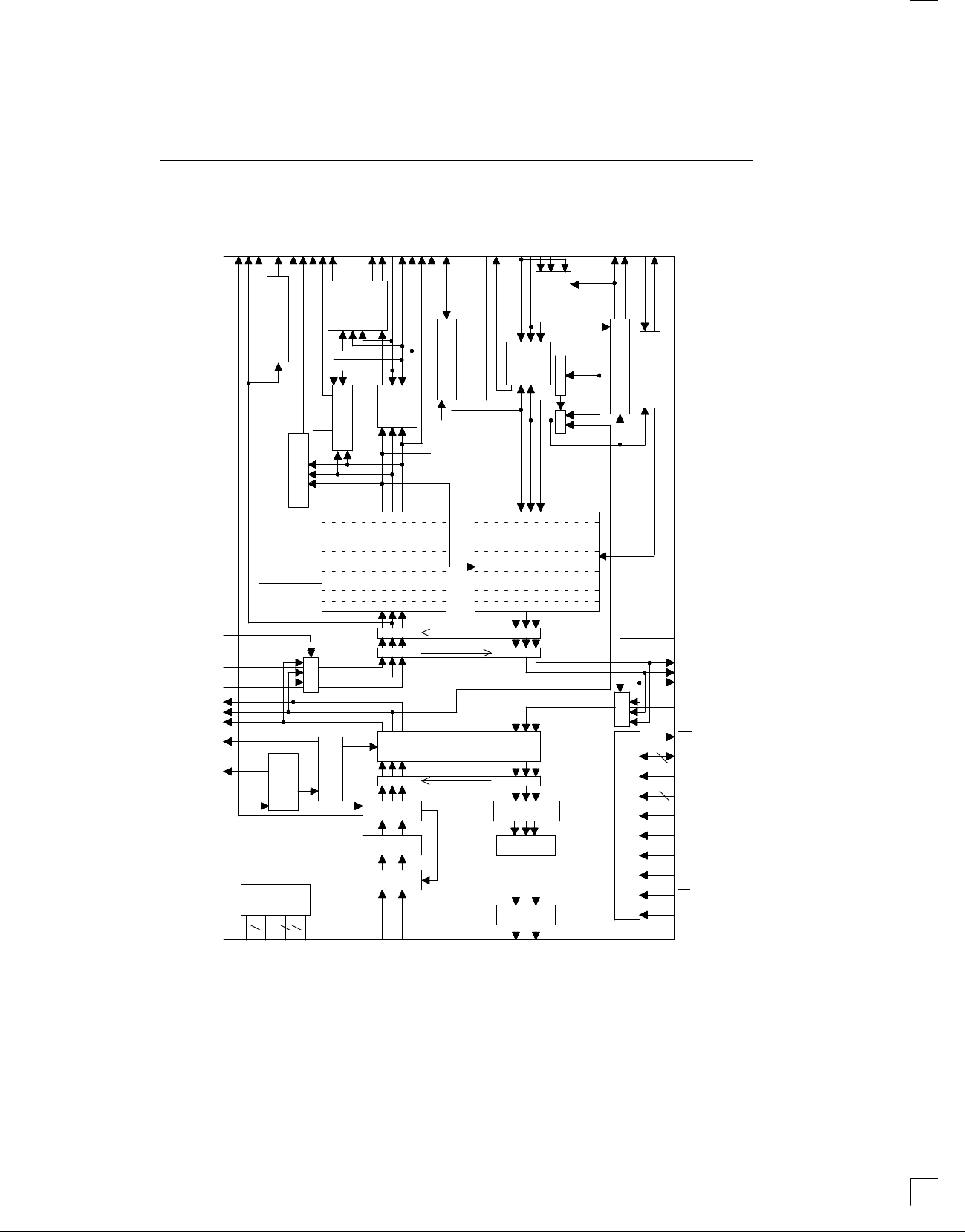
Dallas Semiconductor DS2154 User manual

DS2154
Enhanced E1 Single Chip Transceiver
DS2154
071498 1/71
FEATURES
•CompleteE1(CEPT)PCM–30/ISDN–PRItransceiver
functionality
•Onboard long and short haul line interface for clock/
data recovery and waveshaping
•32–bit or 128–bit crystal–less jitter attenuator
•Generateslinebuildoutsforboth120Ωand75Ωlines
•Frames to FAS, CAS, and CRC4 formats
•Dualonboardtwo–frameelasticstore slipbuffersthat
can connect to asynchronous backplanes up to
8.192 MHz
•8–bit parallel control port that can be used directly on
either multiplexed or non–multiplexed buses
•Extracts and inserts CAS signaling
•Detects and generates Remote and AIS alarms
•Programmable output clocks for Fractional E1, H0,
and H12 applications
•Fully independent transmit and receive functionality
•Full access to both Si and Sa bits aligned with CRC
multiframe
•Four separate loopbacks for testing functions
•Largecounters forbipolar andcode violations, CRC4
codeword errors, FAS errors, and E bits
•Pin compatible with DS2152 T1 Enhanced Single–
Chip Transceiver
•5V supply; low power CMOS
•100–pin 14mm2body LQFP package
PACKAGE OUTLINE
100
1
ORDERING INFORMATION
DS2154L (0°C to 70°C)
DS2154LN (–40°C to +85°C)
DESCRIPTION
The DS2154 Enhanced Single–Chip Transceiver
(ESCT) contains all of the necessary functions for con-
nectiontoE1lines. Thedeviceisanupwardcompatible
version of the DS2153 Single–Chip Transceiver. The
onboard clock/data recovery circuitry coverts the AMI/
HDB3 E1 waveforms to a NRZ serial stream. The
DS2154 automatically adjusts to E1 22AWG (0.6 mm)
twisted–pair cables from 0 to over 2km in length. The
devicecangeneratethe necessaryG.703 waveshapes
forboth 75 ohm coax and120ohm twisted cables. The
onboard jitter attenuator (selectable to either 32 bits or
128 bits) can be placed in either the transmit or receive
data paths. The framer locates the frame and multi-
frame boundaries and monitors the data stream for
alarms. It is also used for extracting and inserting
signaling data, Si, and Sa bit information. The device
contains a set of internal registers which the user can
accesstocontroltheoperationoftheunit. Quickaccess
via the parallel control port allows a single controller to
handle many E1 lines. The device fully meets all of the
latest E1 specifications including ITU G.703, G.704,
G.706,G.823,G.932,andI.431aswellasETS300011,
300 233, 300 166, TBR 12 and TBR 13.

TABLE OF CONTENTS
DS2154
071498 2/71
I.0 INTRODUCTION . . . . . . . . . . . . . . . . . . . . . . . . . . . . . . . . . . . . . . . . . . . . . . . . . . . . . . . . . . . . . . . . . . .
New Features . . . . . . . . . . . . . . . . . . . . . . . . . . . . . . . . . . . . . . . . . . . . . . . . . . . . . . . . . . . . . . . . . . . . . . . . . . . . . . . . . . .
Block Diagram . . . . . . . . . . . . . . . . . . . . . . . . . . . . . . . . . . . . . . . . . . . . . . . . . . . . . . . . . . . . . . . . . . . . . . . . . . . . . . . . . .
Pin List . . . . . . . . . . . . . . . . . . . . . . . . . . . . . . . . . . . . . . . . . . . . . . . . . . . . . . . . . . . . . . . . . . . . . . . . . . . . . . . . . . . . . . . . .
Pin Description . . . . . . . . . . . . . . . . . . . . . . . . . . . . . . . . . . . . . . . . . . . . . . . . . . . . . . . . . . . . . . . . . . . . . . . . . . . . . . . . . .
Register Map . . . . . . . . . . . . . . . . . . . . . . . . . . . . . . . . . . . . . . . . . . . . . . . . . . . . . . . . . . . . . . . . . . . . . . . . . . . . . . . . . . . .
2.0 PARALLEL PORT . . . . . . . . . . . . . . . . . . . . . . . . . . . . . . . . . . . . . . . . . . . . . . . . . . . . . . . . . . . . . . . . . .
3.0 CONTROL, ID, AND TEST REGISTERS . . . . . . . . . . . . . . . . . . . . . . . . . . . . . . . . . . . . . . . . . . . . . . .
SYNC/RESYNC Criteria . . . . . . . . . . . . . . . . . . . . . . . . . . . . . . . . . . . . . . . . . . . . . . . . . . . . . . . . . . . . . . . . . . . . . . . . . .
Framers Loopback . . . . . . . . . . . . . . . . . . . . . . . . . . . . . . . . . . . . . . . . . . . . . . . . . . . . . . . . . . . . . . . . . . . . . . . . . . . . . . .
Automatic Alarm Generation . . . . . . . . . . . . . . . . . . . . . . . . . . . . . . . . . . . . . . . . . . . . . . . . . . . . . . . . . . . . . . . . . . . . . .
Power–up Sequence . . . . . . . . . . . . . . . . . . . . . . . . . . . . . . . . . . . . . . . . . . . . . . . . . . . . . . . . . . . . . . . . . . . . . . . . . . . . .
Remote Loopback . . . . . . . . . . . . . . . . . . . . . . . . . . . . . . . . . . . . . . . . . . . . . . . . . . . . . . . . . . . . . . . . . . . . . . . . . . . . . . .
Local Loopback . . . . . . . . . . . . . . . . . . . . . . . . . . . . . . . . . . . . . . . . . . . . . . . . . . . . . . . . . . . . . . . . . . . . . . . . . . . . . . . . .
4.0 STATUS AND INFORMATION REGISTERS . . . . . . . . . . . . . . . . . . . . . . . . . . . . . . . . . . . . . . . . . . . .
CRC 4 SYNC Counter . . . . . . . . . . . . . . . . . . . . . . . . . . . . . . . . . . . . . . . . . . . . . . . . . . . . . . . . . . . . . . . . . . . . . . . . . . . .
Alarm Criteria . . . . . . . . . . . . . . . . . . . . . . . . . . . . . . . . . . . . . . . . . . . . . . . . . . . . . . . . . . . . . . . . . . . . . . . . . . . . . . . . . . .
5.0 ERROR COUNT REGISTERS . . . . . . . . . . . . . . . . . . . . . . . . . . . . . . . . . . . . . . . . . . . . . . . . . . . . . . . .
BPV or Code Violation Counter . . . . . . . . . . . . . . . . . . . . . . . . . . . . . . . . . . . . . . . . . . . . . . . . . . . . . . . . . . . . . . . . . . . .
CRC4 Error Counter . . . . . . . . . . . . . . . . . . . . . . . . . . . . . . . . . . . . . . . . . . . . . . . . . . . . . . . . . . . . . . . . . . . . . . . . . . . . .
E–bit Counter . . . . . . . . . . . . . . . . . . . . . . . . . . . . . . . . . . . . . . . . . . . . . . . . . . . . . . . . . . . . . . . . . . . . . . . . . . . . . . . . . . .
FAS Error Counter . . . . . . . . . . . . . . . . . . . . . . . . . . . . . . . . . . . . . . . . . . . . . . . . . . . . . . . . . . . . . . . . . . . . . . . . . . . . . . .
6.0 DSO MONITORING FUNCTION . . . . . . . . . . . . . . . . . . . . . . . . . . . . . . . . . . . . . . . . . . . . . . . . . . . . . .
7.0 SIGNALING OPERATION . . . . . . . . . . . . . . . . . . . . . . . . . . . . . . . . . . . . . . . . . . . . . . . . . . . . . . . . . . .
Processor Based Signaling . . . . . . . . . . . . . . . . . . . . . . . . . . . . . . . . . . . . . . . . . . . . . . . . . . . . . . . . . . . . . . . . . . . . . . . .
Hardware Based Signaling . . . . . . . . . . . . . . . . . . . . . . . . . . . . . . . . . . . . . . . . . . . . . . . . . . . . . . . . . . . . . . . . . . . . . . . .
8.0 PER–CHANNEL CODE GENERATION . . . . . . . . . . . . . . . . . . . . . . . . . . . . . . . . . . . . . . . . . . . . . . . .
Transmit Side Code Generation . . . . . . . . . . . . . . . . . . . . . . . . . . . . . . . . . . . . . . . . . . . . . . . . . . . . . . . . . . . . . . . . . . . .
Receive Side Code Generation . . . . . . . . . . . . . . . . . . . . . . . . . . . . . . . . . . . . . . . . . . . . . . . . . . . . . . . . . . . . . . . . . . . .
9.0 CLOCK BLOCKING REGISTERS . . . . . . . . . . . . . . . . . . . . . . . . . . . . . . . . . . . . . . . . . . . . . . . . . . . .
10.0 ELASTIC STORES OPERATION . . . . . . . . . . . . . . . . . . . . . . . . . . . . . . . . . . . . . . . . . . . . . . . . . . . . .
11.0 ADDITIONAL (Sa) AND INTERNATIONAL (Si) BIT OPERATION . . . . . . . . . . . . . . . . . . . . . . . . .
Hardware Scheme . . . . . . . . . . . . . . . . . . . . . . . . . . . . . . . . . . . . . . . . . . . . . . . . . . . . . . . . . . . . . . . . . . . . . . . . . . . . . . .
Internal Register Scheme Based on Double–Frame . . . . . . . . . . . . . . . . . . . . . . . . . . . . . . . . . . . . . . . . . . . . . . . . . .
Internal Register Scheme Based on CRC4 Multiframe . . . . . . . . . . . . . . . . . . . . . . . . . . . . . . . . . . . . . . . . . . . . . . . .

DS2154
071498 3/71
12.0 LINE INTERFACE FUNCTIONS . . . . . . . . . . . . . . . . . . . . . . . . . . . . . . . . . . . . . . . . . . . . . . . . . . . . . .
Receive Clock and Data Recovery . . . . . . . . . . . . . . . . . . . . . . . . . . . . . . . . . . . . . . . . . . . . . . . . . . . . . . . . . . . . . . . . .
Transmit Waveshaping and Line Driving . . . . . . . . . . . . . . . . . . . . . . . . . . . . . . . . . . . . . . . . . . . . . . . . . . . . . . . . . . . .
Jitter Attenuator . . . . . . . . . . . . . . . . . . . . . . . . . . . . . . . . . . . . . . . . . . . . . . . . . . . . . . . . . . . . . . . . . . . . . . . . . . . . . . . . .
13.0 TIMING DIAGRAMS . . . . . . . . . . . . . . . . . . . . . . . . . . . . . . . . . . . . . . . . . . . . . . . . . . . . . . . . . . . . . . . .
Synchronization Flowchart . . . . . . . . . . . . . . . . . . . . . . . . . . . . . . . . . . . . . . . . . . . . . . . . . . . . . . . . . . . . . . . . . . . . . . . .
Transmit Data Flow Diagram . . . . . . . . . . . . . . . . . . . . . . . . . . . . . . . . . . . . . . . . . . . . . . . . . . . . . . . . . . . . . . . . . . . . . .
14.0 CHARACTERISTICS . . . . . . . . . . . . . . . . . . . . . . . . . . . . . . . . . . . . . . . . . . . . . . . . . . . . . . . . . . . . . . . .
Absolute Maximum Ratings . . . . . . . . . . . . . . . . . . . . . . . . . . . . . . . . . . . . . . . . . . . . . . . . . . . . . . . . . . . . . . . . . . . . . . .
DC Parameters . . . . . . . . . . . . . . . . . . . . . . . . . . . . . . . . . . . . . . . . . . . . . . . . . . . . . . . . . . . . . . . . . . . . . . . . . . . . . . . . . .
AC Parameters . . . . . . . . . . . . . . . . . . . . . . . . . . . . . . . . . . . . . . . . . . . . . . . . . . . . . . . . . . . . . . . . . . . . . . . . . . . . . . . . . .
Timing . . . . . . . . . . . . . . . . . . . . . . . . . . . . . . . . . . . . . . . . . . . . . . . . . . . . . . . . . . . . . . . . . . . . . . . . . . . . . . . . . . . . . . . . .
Package Description . . . . . . . . . . . . . . . . . . . . . . . . . . . . . . . . . . . . . . . . . . . . . . . . . . . . . . . . . . . . . . . . . . . . . . . . . . . . .

DS2154
071498 4/71
1.0 INTRODUCTION
The DS2154 is a super–set version of the popular
DS2153 E1 Single–Chip Transceiver offering the new
features listed below. All of the original features of the
DS2153 have been retained and software created for
the original devices is transferrable into the DS2154.
NEW FEATURES SECTION
Option for non–multiplexed bus operation 1 and 2
Crystal–less jitter attenuation 12
Additional hardware signaling capability including:
Receive signaling reinsertion to a backplane multiframe sync
Availability of signaling in a separate PCM data stream
Signaling freezing
Interrupt generated on change of signaling data
7
Improved receive sensitivity: 0 dB to –43 dB 12
Per–channel code insertion in both transmit and receive paths 8
Expanded access to Sa and Si bits 11
RCL, RLOS, RRA, and RAIS alarms now interrupt on change of state 4
8.192 MHz clock synthesizer 1
Per–channel loopback 8
Addition of hardware pins to indicate carrier loss and signaling freeze 1
Line interface function can be completely decoupled from the framer/formatter to
allow:
Interface to optical, HDSL, and other NRZ interfaces
“tap” the transmit and receive bipolar data streams for monitoring purposes
Be able corrupt data and insert framing errors, CRC errors, etc.
1
Transmit and receive elastic stores now have independent backplane clocks 1
Ability to monitor one DS0 channel in both the transmit and receive paths 6
Access to the data streams in between the framer/formatter and the elastic stores 1
AIS generation in the line interface that is independent of loopbacks 1 and 3
Transmit current limiter to meet the 50 mA short circuit requirement 12
Option to extend carrier loss criteria to a 1 ms period as per ETS 300 233 3
Automatic RAI generation to ETS 300 011 specifications 3

DS2154
071498 5/71
DS2154 ENHANCED E1 SINGLE–CHIP TRANSCEIVER Figure 1–1
8
VCO/ PLL
7
4
3
4
RCL
RCLK
RLOS
8MCLK
RLINK
RLCLK
RCHBLK
RCHCLK
RSIGF
RSIG
RSER
RSYSCLK
RSYNC
RMSYNC
RFSYNC
RDATA
TSYNC
TDATA
TESO
TSSYNC
TSYSCLK
TSER
TSIG
TCLK
TCHBLK
TCHCLK
TLINK
TLCLK
SIGNALING
BUFFER
8.192 MHz CLOCK
SYNTHESIZER
TIMING
CONTROL
Sa EXTRACTION
ELASTIC
STORE
SYNC CONTROL
HARDWARE
SIGNALING
INSERTION
ELASTIC
STORE
TIMING CONTROL
Sa INSERTION
LOTCMUX
SYNC
CLOCK
DATA
SYNC
CLOCK
DATA
RECEIVE SIDE
FRAMER
TRANSMIT
SIDE
FORMATTER
FRAMER LOOPBACK
REMOTE LOOPBACK
PER–CHANNEL CODE INSERT
FAS WORD INSERTION
SI BIT INSERTION
E–BIT INSERTION
SA INSERTION
PER–CHANNEL LOOPBACK
SIGNALING INSERTION
CRC4 GENERAITON
HDB3 ENCODE
AIS GENERAITON
PER–CHANNEL CODE INSERT
SAAND SI EXTRACTION
SIGNALING EXTRACTION
E–BIT COUNTER
FAS ERROR COUNTER
CRC ERROR COUNTER
ALARM DETECTION
SYNCHRONIZER
BPV COUNTER
HDB3 DECODER
LIUC
MUX
JITTER ATTENUATION
(CAN BE PLACED IN EITHER
TRANSMIT OR RECEIVE PATH)
16.384 MHz
LOCAL LOOPBACK
POWER
CONNECTIONS
CLOCK/DATA
RECOVERY
PEAK
EQUALIZER
DETECT
LIU AIS
GENERATION
WAVE–
SHAPING
LINE
DRIVERS
PARALLEL AND TEST CONTROL PORT
(ROUTED TO ALL BLOCKS) MUX
CLOCK/
CRYSTAL
INTERFACE
2.048
MHz
32.768 MHz
LIUC
TPOSO
TCLKO
TNEGO
TNEGI
TCLKI
TPOSI
MUX
D0 to D7/
AD0 to AD7
A0 to A6
ALE(AS)/A7
RD(DS)
WR(R/W)
BTS
CS
TEST
INT
RPOSI
RCLKI
RNEGI
RNEGO
RCLKO
RPOSO
8XCLK
XTALD
MCLK
RVDD
DVDD
TVDD
RVSS
DVSS
TVSS
RRING
RTIP
TRING
TTIP
LOTC

DS2154
071498 6/71
FUNCTIONAL DESCRIPTION
The analog AMI/HDB3 waveform off of the E1 line is
transformer coupled into the RRING and RTIP pins of
the DS2154. The device recovers clock and data from
theanalogsignal andpasses itthroughthe jitterattenu-
ation mux to the receive side framer where the digital
serial stream is analyzed to locate the framing/multi-
framepattern. TheDS2154containsanactivefilterthat
reconstructs the analog received signal for the non–lin-
earlosses thatoccur in transmission. Thedevice has a
usablereceivesensitivityof0dBto–43dBwhichallows
thedevicetooperateoncablesover2kminlength. The
receivesideframerlocatestheFASframeandCRCand
CASmultiframeboundariesaswellasdetectsincoming
alarms including, carrier loss, loss of synchronization,
AIS, and Remote Alarm. If needed, the receive side
elastic store can be enabled in order to absorb the
phase and frequency differences between the recov-
ered E1 data stream and an asynchronous backplane
clock which is provided at the RSYSCLK input. The
clock applied at the RSYSCLK input can be either a
2.048MHz clock or a1.544 MHz clock. The RSYSCLK
canalsobeaburstyclockwithspeedsupto8.192MHz.
The transmit side of the DS2154 is totally independent
fromthereceivesideinboththeclockrequirementsand
characteristics. Data off of a backplane can be passed
through a transmit side elastic store if necessary. The
transmitformatterwillprovidethenecessaryframe/mul-
tiframe data overhead for E1 transmission. Once the
data stream has been prepared for transmission, it is
sent via the jitter attenuation mux to the waveshaping
and line driver functions. The DS2154 will drive the E1
linefrom theTTIP and TRINGpins via acoupling trans-
former. The line driver can handle both 75Ωand
120Ωlines and it has options for high return loss
applications. The line driver contains a current limiter
that will restrict the maximum current into a 1Ωload to
less than 50 mA (rms).
READER’S NOTE
This data sheet assumes a particular nomenclature of
the E1 operating environment. There are 32 eight–bit
timeslots in an E1 systems which are number 0 to 31.
Timeslot 0 is transmitted first and received first. These
32timeslotsarealsoreferredtoaschannelswithanum-
beringschemeof1to32. Timeslot0isidenticaltochan-
nel 1, timeslot 1 is identical to Channel 2, and so on.
Eachtimeslot(orchannel)ismadeupofeightbitswhich
are numbered 1 to 8. Bit number 1 is the MSB and is
transmitted first. Bit number 8 is the LSB and is trans-
mitted last. Throughout this data sheet, the following
abbreviations will be used:
FAS Frame Alignment Sig-
nal CRC4 Cyclical Redundancy
Check
CAS Channel Associated
Signaling CCS Common Channel
Signaling
MF Multiframe Sa Additional bits
Si International bits E–bit CRC4 Error bits
PIN LIST Table 1–1
PIN SYMBOL TYPE DESCRIPTION
1 RCHBLK O Receive Channel Block.
2 NC – No Connect.
3 8MCLK O 8.192 MHz Clock.
4 NC – No Connect.
5 NC – No Connect.
6 RCL O Receive Carrier Loss.
7 NC – No Connect.
8 NC – No Connect.

DS2154
071498 7/71
PIN DESCRIPTIONTYPESYMBOL
9 NC – No Connect.
10 NC – No Connect.
11 BTS I Bus Type Select.
12 LIUC I Line Interface Connect.
13 8XCLK O Eight Times Clock.
14 TEST I Test.
15 NC – No Connect.
16 RTIP I Receive Analog Tip Input.
17 RRING I Receive Analog Ring Input.
18 RVDD – Receive Analog Positive Supply.
19 RVSS – Receive Analog Signal Ground.
20 RVSS – Receive Analog Signal Ground.
21 MCLK I Master Clock Input.
22 XTALD O Quartz Crystal Driver.
23 NC – No Connect.
24 RVSS – Receive Analog Signal Ground.
25 INT O Interrupt.
26 NC – No Connect.
27 NC – No Connect.
28 NC – No Connect.
29 TTIP O Transmit Analog Tip Output.
30 TVSS – Transmit Analog Signal Ground.
31 TVDD – Transmit Analog Positive Supply.
32 TRING O Transmit Analog Ring Output.
33 TCHBLK O Transmit Channel Block.
34 TLCLK O Transmit Link Clock.
35 TLINK I Transmit Link Data.
36 NC – No Connect.
37 TSYNC I/O Transmit Sync.
38 TPOSI I Transmit Positive Data Input.
39 TNEGI I Transmit Negative Data Input.
40 TCLKI I Transmit Clock Input.
41 TCLKO O Transmit Clock Output.
42 TNEGO O Transmit Negative Data Output.
43 TPOSO O Transmit Positive Data Output.

DS2154
071498 8/71
PIN DESCRIPTIONTYPESYMBOL
44 DVDD – Digital Positive Supply.
45 DVSS – Digital Signal Ground.
46 TCLK I Transmit Clock.
47 TSER I Transmit Serial Data.
48 TSIG I Transmit Signaling Input.
49 TESO O Transmit Elastic Store Output.
50 TDATA I Transmit Data.
51 TSYSCLK I Transmit System Clock.
52 TSSYNC I Transmit System Sync.
53 TCHCLK O Transmit Channel Clock.
54 NC – No Connect.
55 MUX I Bus Operation.
56 D0/AD0 I/O Data Bus Bit 0 / Address/Data Bus Bit 0.
57 D1/AD1 I/O Data Bus Bit 1 / Address/Data Bus Bit 1.
58 D2/AD2 I/O Data Bus Bit 2 / Address/Data Bus Bit 2.
59 D3/AD3 I/O Data Bus Bit 3 / Address/Data Bus Bit 3.
60 DVSS – Digital Signal Ground.
61 DVDD – Digital Positive Supply.
62 D4/AD4 I/O Data Bus Bit 4 / Address/Data Bus Bit 4.
63 D5/AD5 I/O Data Bus Bit 5 / Address/Data Bus Bit 5.
64 D6/AD6 I/O Data Bus Bit 6 / Address/Data Bus Bit 6.
65 D7/AD7 I/O Data Bus Bit 7 / Address/Data Bus Bit 7.
66 A0 I Address Bus Bit 0.
67 A1 I Address Bus Bit 1.
68 A2 I Address Bus Bit 2.
69 A3 I Address Bus Bit 3.
70 A4 I Address Bus Bit 4.
71 A5 I Address Bus Bit 5.
72 A6 I Address Bus Bit 6.
73 A7/ALE I Address Bus Bit 7 / Address Latch Enable.
74 RD (DS) I Read Input (Data Strobe).
75 CS I Chip Select.
76 NC – No Connect.
77 WR (R/W) I Write Input (Read/Write).
78 RLINK O Receive Link Data.

DS2154
071498 9/71
PIN DESCRIPTIONTYPESYMBOL
79 RLCLK O Receive Link Clock.
80 DVSS – Digital SIgnal Ground.
81 DVDD – Digital Positive Supply.
82 RCLK O Receive Clock.
83 DVDD – Digital Positive Supply.
84 DVSS – Digital Signal Ground.
85 RDATA O Receive Data.
86 RPOSI I Receive Positive Data Input.
87 RNEGI I Receive Negative Data Input.
88 RCLKI I Receive Clock Input.
89 RCLKO O Receive Clock Output.
90 RNEGO O Receive Negative Data Output.
91 RPOSO O Receive Positive Data Output.
92 RCHCLK O Receive Channel Clock.
93 RSIGF O Receive Signaling Freeze Output.
94 RSIG O Receive Signaling Output.
95 RSER O Receive Serial Data.
96 RMSYNC O Receive Multiframe Sync.
97 RFSYNC O Receive Frame Sync.
98 RSYNC I/O Receive Sync.
99 RLOS/LOTC O Receive Loss Of Sync / Loss Of Transmit Clock.
100 RSYSCLK I Receive System Clock.
NOTE:
Leave all no connect (NC) pins open circuited.
DS2154 PIN DESCRIPTION Table 1–2
TRANSMIT SIDE DIGITAL PINS
Transmit Clock [TCLK]. A 2.048 MHz primary clock.
Used to clock data through the transmit side formatter.
Must be present for the parallel control port to operate
properly. If not present, the Loss Of Transmit Clock
(LOTC) function can provide a clock.
Transmit Serial Data [TSER]. Transmit NRZ serial
data. Sampled on the falling edge of TCLK when the
transmit side elastic store is disabled. Sampled on the
fallingedge ofTSYSCLK when the transmitside elastic
store is enabled.
TransmitChannelClock[TCHCLK]. A256KHzclock
whichpulseshighduringtheLSBofeachchannel. Syn-
chronous with TCLK when the transmit side elastic
store is disabled. Synchronous with TSYSCLK when
thetransmitsideelasticstoreisenabled. Usefulforpar-
allel to serial conversion of channel data.
TransmitChannelBlock[TCHBLK]. Auser program-
mableoutputthatcanbeforcedhighorlowduringanyof
the 32 E1 channels. Synchronous with TCLK when the
transmit side elastic store is disabled. Synchronous
with TSYSCLK when the transmit side elastic store is

DS2154
071498 10/71
enabled. Useful for blocking clocks to a serial UART or
LAPD controller in applications where not all E1 chan-
nels are used such as Fractional E1, 384 Kbps (H0),
768 Kbps, 1920 Kbps (H12) or ISDN–PRI. Also useful
for locating individual channels in drop–and–insert
applications,forexternalper–channelloopback,andfor
per–channel conditioning. See Section 9 for details.
Transmit System Clock [TSYSCLK]. 1.544 MHz or
2.048 MHz clock. Only used when the transmit side
elastic store function is enabled. Should be tied low in
applications that do not use the transmit side elastic
store. Can be burst at rates up to 8.192 MHz.
Transmit Link Clock [TLCLK]. 4 KHz to 20 KHz
demandclock(Sabits)fortheTLINKinput. SeeSection
11 for details.
TransmitLinkData[TLINK]. Ifenabled,thispinwillbe
sampled on the falling edge of TCLK for data insertion
into any combination of the Sa bit positions (Sa4 to
Sa8). See Section 11 for details.
Transmit Sync [TSYNC]. Apulseat this pinwill estab-
lisheitherframe or multiframe boundaries for the trans-
mit side. This pin can also be programmed to output
eitheraframeormultiframepulse. Alwayssynchronous
with TCLK.
TransmitFrameSync[TSSYNC]. Onlyusedwhenthe
transmitsideelasticstoreisenabled. Apulse atthispin
will establish either frame or multiframe boundaries for
thetransmitside. Shouldbetiedlowinapplicationsthat
do not use the transmit side elastic store. Always syn-
chronous with TSYSCLK.
Transmit Signaling Input [TSIG]. When enabled, this
input will be sample signaling bits for insertion into out-
going PCM E1 data stream. Sampled on the falling
edgeofTCLKwhenthetransmitsideelasticstoreisdis-
abled. Sampled on the falling edge of TSYSCLK when
the transmit side elastic store is enabled. See Section
13 for timing examples.
Transmit Elastic Store Data Output [TESO].
Updatedon therising edge ofTCLK with dataoutof the
the transmit side elastic store whether the elastic store
is enabled or not. This pin is normally tied to TDATA.
Transmit Data [TDATA]. Sampled on the falling edge
of TCLK with data to be clocked through the transmit
side formatter. This pin is normally tied to TESO.
TransmitPositiveDataOutput[TPOSO]. Updatedon
therisingedgeofTCLKOwiththebipolardataoutofthe
transmit side formatter. Can be programmed to source
NRZ data via the Output Data Format (TCR1.7) control
bit. This pin is normally tied to TPOSI.
Transmit Negative Data Output [TNEGO]. Updated
onthe risingedgeof TCLKO withthe bipolar dataout of
the transmit side formatter. This pin is normally tied to
TNEGI.
Transmit Clock Output [TCLKO]. Buffered clock that
isused toclockdata throughthetransmit sideformatter
(i.e.either TCLK orRCLKO if Loss OfTransmitClock is
enabled and in effect or RCLKI if remote loopback is
enabled). This pin is normally tied to TCLKI.
Transmit Positive Data Input [TPOSI]. Sampled on
the falling edge of TCLKI for data to be transmitted out
ontotheE1line. CanbeinternallyconnectedtoTPOSO
by tying the LIUC pin high.
Transmit Negative Data Input [TNEGI]. Sampled on
the falling edge of TCLKI for data to be transmitted out
ontotheE1line. CanbeinternallyconnectedtoTNEGO
by tying the LIUC pin high.
Transmit Clock Input [TCLKI]. Line interfacetransmit
clock. Can be internally connected to TCLKO by tying
the LIUC pin high.
RECEIVE SIDE DIGITAL PINS
Receive Link Data [RLINK]. Updated with the full
recovered E1 data stream on the rising edge of RCLK.
Receive Link Clock [RLCLK]. 4 KHz to 20 KHz clock
(Sa bits) for the RLINK output. See Section 11 for
details.
Receive Clock [RCLK]. 2.048 MHz clock that is used
to clock data through the receive side framer.

DS2154
071498 11/71
Receive Channel Clock [RCHCLK]. 256 KHz clock
which pulses high during the LSB of each channel.
Synchronous with RCLK when the receive side elastic
store is disabled. Synchronous with RSYSCLK when
the receive side elastic store is enabled. Useful for par-
allel to serial conversion of channel data.
Receive Channel Block [RCHBLK]. A user program-
mableoutputthatcanbeforcedhighorlowduringanyof
the32 E1channels. Synchronous withRCLK whenthe
receivesideelasticstoreisdisabled. Synchronouswith
RSYSCLK when the receive side elastic store is
enabled. Useful for blocking clocks to a serial UART or
LAPD controller in applications where not all E1 chan-
nels are used such as Fractional E1, 384K bps service,
768Kbps,orISDN–PRI. Alsousefulforlocatingindivid-
ualchannels in drop–and–insert applications,for exter-
nal per–channel loopback, and for per–channel condi-
tioning. See Section 9 for details.
Receive Serial Data [RSER]. Received NRZ serial
data. Updated on rising edges of RCLK when the
receive side elastic store is disabled. Updated on the
risingedgesofRSYSCLK whenthe receiveside elastic
store is enabled.
Receive Sync [RSYNC]. An extracted pulse, one
RCLK wide, is output at this pin which identifies either
frame or CAS/CRC multiframe boundaries. If the
receivesideelasticstoreisenabled,thenthispincanbe
enabled to be an input at which a frame or multiframe
boundarypulsesynchronouswithRSYSCLKisapplied.
Receive Frame Sync [RFSYNC]. An extracted 8 KHz
pulse,one RCLKwide, is outputat this pinwhich identi-
fies frame boundaries.
Receive Multiframe Sync [RMSYNC]. An extracted
pulse, one RSYSCLK wide, is output at this pin which
identifies multiframe boundaries. If the receive side
elasticstoreisdisabled, thenthisoutputwill outputmul-
tiframe boundaries associated with RCLK.
Receive Data [RDATA]. Updated on the rising edge of
RCLK with the data out of the receive side framer.
Receive System Clock [RSYSCLK]. 1.544 MHz or
2.048 MHz clock. Only used when the elastic store
function is enabled. Should be tied low in applications
thatdonotusetheelasticstore. Canbeburstatratesup
to 8.192 MHz.
Receive Signaling Output [RSIG]. Outputs signaling
bitsina PCMformat. Updated onrisingedges ofRCLK
whenthereceivesideelasticstoreisdisabled. Updated
on the rising edges of RSYSCLK when the receive side
elastic store is enabled. See Section 13 for timing
examples.
Receive Loss of Sync / Loss of Transmit Clock
[RLOS/LOTC]. Adual functionoutput thatis controlled
bythe TCR2.0controlbit. This pincan be programmed
toeithertogglehighwhenthesynchronizerissearching
fortheframeandmultiframeortotogglehighiftheTCLK
pin has not been toggled for 5 µs.
Receive Carrier Loss [RCL]. Set high when the line
interface detects a loss of carrier. [Note: a test mode
exists to allow the DS2154 to detect carrier loss at
RPOSI and RNEGI in place of detection at RTIP and
RRING].
ReceiveSignalingFreeze[RSIGF]. Sethighwhenthe
signaling data is frozen via either automatic or manual
intervention. Used to alert downstream equipment of
the condition.
8 MHz Clock [8MCLK]. 8.192 MHz output clock that is
referenced to the clock that is output at the RCLK pin.
Receive Positive Data Output [RPOSO]. Updatedon
therisingedgeofRCLKOwiththebipolardataoutofthe
line interface. This pin is normally tied to RPOSI.
Receive Negative Data Output [RNEGO]. Updated
ontherising edgeofRCLKOwiththe bipolardata outof
the line interface. This pin is normally tied to RNEGI.
Receive Clock Output [RCLKO]. Buffered recovered
clock from the E1 line. This pin is normally tied to
RCLKI.
Receive Positive Data Input [RPOSI]. Sampled on
thefalling edgeof RCLKI fordata tobe clocked through
thereceive sideframer. RPOSI and RNEGIcan be tied
together for a NRZ interface. Can be internally con-
nected to RPOSO by tying the LIUC pin high.
Receive Negative Data Input [RNEGI]. Sampled on
thefalling edgeof RCLKI fordata tobe clocked through
thereceive sideframer. RPOSI and RNEGIcan be tied
together for a NRZ interface. Can be internally con-
nected to RNEGO by tying the LIUC pin high.

DS2154
071498 12/71
Receive Clock Input [RCLKI]. Clock used to clock
data through the receive side framer. This pin is nor-
mally tied to RCLKO. Can be internally connected to
RCLKO by tying the LIUC pin high. RCLKI must be
present for the parallel control port to operate properly.
PARALLEL CONTROL PORT PINS
Interrupt [INT]. Flags host controller during conditions
and change of conditions defined in the Status Regis-
ters 1 and 2. Active low, open drain output.
3–State Control [Test]. Set high to 3–state all output
andI/Opins(includingtheparallelcontrolport). Setlow
for normal operation. Useful in board level testing.
Bus Operation [MUX]. Set low to select non–multi-
plexedbusoperation. Sethightoselectmultiplexedbus
operation.
Data Bus [D0 to D7] or Address/Data Bus [AD0 to
AD7]. In non–multiplexed bus operation (MUX=0),
serves as the data bus. In multiplexed bus operation
(MUX=1), serves as a 8–bit multiplexed address / data
bus.
Address Bus [A0 to A6]. In non–multiplexed bus
operation(MUX=0),serves asthe addressbus. In mul-
tiplexed bus operation (MUX=1), these pins are not
used and should be tied low.
Bus Type Select [BTS]. Strap high to select Motorola
bus timing; strap low to select Intel bus timing. This pin
controls the function of the RD\(DS), ALE(AS), and
WR\(R/W\)pins. If BTS=1, then these pinsassume the
function listed in parenthesis ().
Read Input [RD] (Data Strobe [DS]). RD and DS are
active low signals when MUX=11. DS is active high
when MUX = 0. See bus timing diagrams.
Chip Select [CS]. Must be low to read or write to the
device. CS is an active low signal.
A7 or Address Latch Enable [ALE] (Address Strobe
[AS]). In non–multiplexed bus operation (MUX=0),
serves as the upper address bit. In multiplexed bus
operation (MUX=1), serves to demultiplex the bus on a
positive–going edge.
WriteInput[WR] (Read/Write[R/W]). WRisanactive
low signal.
LINE INTERFACE PINS
Master Clock Input [MCLK]. 2.048 MHz (±50 ppm)
clock source with TTL levels is applied at this pin. This
clockis usedinternallyfor bothclock/data recoveryand
forjitter attenuation. Aquartzcrystal of2.048 MHzmay
beappliedacrossMCLKand XTALDinsteadof theTTL
level clock source.
Quartz Crystal Driver [XTALD]. A quartz crystal of
2.048 MHz may be applied across MCLK and XTALD
instead of a TTL level clock source at MCLK. Leave
opencircuited ifa TTLclock sourceis appliedatMCLK.
EightTimesClock [8XCLK]. 16.384 MHzclock thatis
frequency locked to the 2.048 MHz clock provided from
the clock/data recovery block (if the jitter attenuator is
enabledonthereceiveside)orfromtheTCLKIpin(ifthe
jitterattenuatorisenabledonthetransmitside). Canbe
internallydisabledviathe TEST2registerif notneeded.
LineInterfaceConnect[LIUC]. Tielowtoseparatethe
lineinterfacecircuitryfromtheframer/formattercircuitry
and activate the TPOSI/TNEGI/TCLKI/RPOSI/RNEGI/
RCLKIpins. Tiehightoconnectthethelineinterfacecir-
cuitry to the framer/formatter circuitry and deactivate
the TPOSI/TNEGI/TCLKI/RPOSI/RNEGI/RCLKI pins.
When LIUC is tied high, the TPOSI/TNEGI/TCLKI/
RPOSI/RNEGI/RCLKI pins should be tied low.
Receive Tip and Ring [RTIP and RRING]. Analog
inputs for clock recovery circuitry. These pins connect
via a 1:1 transformer to either the E1 line. See Section
12 for an example.
TransmitTipandRing[TTIPandTRING]. Analogline
driver outputs. These pins connect via a 1:1.15 or
1:1.36 step–up transformer to the E1 line. See Section
12 for an example.
SUPPLY PINS
Digital Positive Supply [DVDD]. 5.0 volts ±5%.
Should be tied to the RVDD and TVDD pins.

DS2154
071498 13/71
Receive Analog Positive Supply [RVDD]. 5.0 volts
±5%. Should be tied to the DVDD and TVDD pins.
Transmit Analog Positive Supply [TVDD]. 5.0 volts
±5%. Should be tied to the RVDD and DVDD pins.
Digital Signal Ground [DVSS]. 0.0 volts. Should be
tied to the RVSS and TVSS pins.
Receive Analog Signal Ground [RVSS]. 0.0 volts.
Should be tied to the DVSS and TVSS pins.
Transmit Analog Ground [TVSS]. 0.0 volts. Should
be tied to the RVSS and DVSS pins.
DS2154 REGISTER MAP Table 1–3
ADDRESS R/W REGISTER NAME REGISTER ABBREVIATION
00 R BPV or Code Violation Count 1. VCR1
01 R BPV or Code Violation Count 2. VCR2
02 R CRC4 Error Count 1 / FAS Error Count 1. CRCCR1
03 R CRC4 Error Count 2. CRCCR2
04 R E–Bit Count 1 / FAS Error Count 2. EBCR1
05 R E–Bit Count 2. EBCR2
06 R/W Status 1. SR1
07 R/W Status 2. SR2
08 R/W Receive Information. RIR
09 – not present. –
0A – not present. –
0B – not present. –
0C – not present. –
0D – not present. –
0E – not present. –
0F R Device ID Register. IDR
10 R/W Receive Control 1. RCR1
11 R/W Receive Control 2. RCR2
12 R/W Transmit Control 1. TCR1
13 R/W Transmit Control 2. TCR2
14 R/W Common Control 1. CCR1
15 R/W Test 1. TEST1 (set to 00h)
16 R/W Interrupt Mask 1. IMR1
17 R/W Interrupt Mask 2. IMR2
18 R/W Line Interface Control. LICR
19 R/W Test 2. TEST2 (set to 00h)

DS2154
071498 14/71
ADDRESS REGISTER ABBREVIATIONREGISTER NAMER/W
1A R/W Common Control 2. CCR2
1B R/W Common Control 3. CCR3
1C R/W Transmit Sa Bit Control. TSaCR
1D – Not present. –
1E R Synchronizer Status. SSR
1F R Receive Non–Align Frame. RNAF
20 R/W Transmit Align Frame. TAF
21 R/W Transmit Non–Align Frame. TNAF
22 R/W Transmit Channel Blocking 1. TCBR1
23 R/W Transmit Channel Blocking 2. TCBR2
24 R/W Transmit Channel Blocking 3. TCBR3
25 R/W Transmit Channel Blocking 4. TCBR4
26 R/W Transmit Idle 1. TIR1
27 R/W Transmit Idle 2. TIR2
28 R/W Transmit Idle 3. TIR3
29 R/W Transmit Idle 4. TIR4
2A R/W Transmit Idle Definition. TIDR
2B R/W Receive Channel Blocking 1. RCBR1
2C R/W Receive Channel Blocking 2. RCBR2
2D R/W Receive Channel Blocking 3. RCBR3
2E R/W Receive Channel Blocking 4. RCBR4
2F R Receive Align Frame. RAF
30 R Receive Signaling 1. RS1
31 R Receive Signaling 2. RS2
32 R Receive Signaling 3. RS3
33 R Receive Signaling 4. RS4
34 R Receive Signaling 5. RS5
35 R Receive Signaling 6. RS6
36 R Receive Signaling 7. RS7
37 R Receive Signaling 8. RS8
38 R Receive Signaling 9. RS9
39 R Receive Signaling 10. RS10
3A R Receive Signaling 11. RS11

DS2154
071498 15/71
ADDRESS REGISTER ABBREVIATIONREGISTER NAMER/W
3B R Receive Signaling 12. RS12
3C R Receive Signaling 13. RS13
3D R Receive Signaling 14. RS14
3E R Receive Signaling 15. RS15
3F R Receive Signaling 16. RS16
40 R/W Transmit Signaling 1. TS1
41 R/W Transmit Signaling 2. TS2
42 R/W Transmit Signaling 3. TS3
43 R/W Transmit Signaling 4. TS4
44 R/W Transmit Signaling 5. TS5
45 R/W Transmit Signaling 6. TS6
46 R/W Transmit Signaling 7. TS7
47 R/W Transmit Signaling 8. TS8
48 R/W Transmit Signaling 9. TS9
48 R/W Transmit Signaling 10. TS10
4A R/W Transmit Signaling 11. TS11
4B R/W Transmit Signaling 12. TS12
4C R/W Transmit Signaling 13. TS13
4D R/W Transmit Signaling 14. TS14
4E R/W Transmit Signaling 15. TS15
4F R/W Transmit Signaling 16. TS16
50 R/W Transmit Si Bits Align Frame. TSiAF
51 R/W Transmit Si Bits Non–Align Frame. TSiNAF
52 R/W Transmit Remote Alarm Bits. TRA
53 R/W Transmit Sa4 Bits. TSa4
54 R/W Transmit Sa5 Bits. TSa5
55 R/W Transmit Sa6 Bits. TSa6
56 R/W Transmit Sa7 Bits. TSa7
57 R/W Transmit Sa8 Bits. TSa8
58 R Receive Si Bits Align Frame. RSiAF
59 R Receive Si Bits Non–Align Frame. RSiNAF
5A R Receive Remote Alarm Bits. RRA
5B R Receive Sa4 Bits. RSa4

DS2154
071498 16/71
ADDRESS REGISTER ABBREVIATIONREGISTER NAMER/W
5C R Receive Sa5 Bits. RSa5
5D R Receive Sa6 Bits. RSa6
5E R Receive Sa7 Bits. RSa7
5F R Receive Sa8 Bits. RSa8
60 R/W Transmit Channel 1. TC1
61 R/W Transmit Channel 2. TC2
62 R/W Transmit Channel 3. TC3
63 R/W Transmit Channel 4. TC4
64 R/W Transmit Channel 5. TC5
65 R/W Transmit Channel 6. TC6
66 R/W Transmit Channel 7. TC7
67 R/W Transmit Channel 8. TC8
68 R/W Transmit Channel 9. TC9
69 R/W Transmit Channel 10. TC10
6A R/W Transmit Channel 11. TC11
6B R/W Transmit Channel 12. TC12
6C R/W Transmit Channel 13. TC13
6D R/W Transmit Channel 14. TC14
6E R/W Transmit Channel 15. TC15
6F R/W Transmit Channel 16. TC16
70 R/W Transmit Channel 17. TC17
71 R/W Transmit Channel 18. TC18
72 R/W Transmit Channel 19. TC19
73 R/W Transmit Channel 20. TC20
74 R/W Transmit Channel 21. TC21
75 R/W Transmit Channel 22. TC22
76 R/W Transmit Channel 23. TC23
77 R/W Transmit Channel 24. TC24
78 R/W Transmit Channel 25. TC25
79 R/W Transmit Channel 26. TC26
7A R/W Transmit Channel 27. TC27
7B R/W Transmit Channel 28. TC28
7C R/W Transmit Channel 29. TC29

DS2154
071498 17/71
ADDRESS REGISTER ABBREVIATIONREGISTER NAMER/W
7D R/W Transmit Channel 30. TC30
7E R/W Transmit Channel 31. TC31
7F R/W Transmit Channel 32. TC32
80 R/W Receive Channel 1. RC1
81 R/W Receive Channel 2. RC2
82 R/W Receive Channel 3. RC3
83 R/W Receive Channel 4. RC4
84 R/W Receive Channel 5. RC5
85 R/W Receive Channel 6. RC6
86 R/W Receive Channel 7. RC7
87 R/W Receive Channel 8. RC8
88 R/W Receive Channel 9. RC9
89 R/W Receive Channel 10. RC10
8A R/W Receive Channel 11. RC11
8B R/W Receive Channel 12. RC12
8C R/W Receive Channel 13. RC13
8D R/W Receive Channel 14. RC14
8E R/W Receive Channel 15. RC15
8F R/W Receive Channel 16. RC16
90 R/W Receive Channel 17. RC17
91 R/W Receive Channel 18. RC18
92 R/W Receive Channel 19. RC19
93 R/W Receive Channel 20. RC20
94 R/W Receive Channel 21. RC21
95 R/W Receive Channel 22. RC22
96 R/W Receive Channel 23. RC23
97 R/W Receive Channel 24. RC24
98 R/W Receive Channel 25. RC25
99 R/W Receive Channel 26. RC26
9A R/W Receive Channel 27. RC27
9B R/W Receive Channel 28. RC28
9C R/W Receive Channel 29. RC29
9D R/W Receive Channel 30. RC30

DS2154
071498 18/71
ADDRESS REGISTER ABBREVIATIONREGISTER NAMER/W
9E R/W Receive Channel 31. RC31
9F R/W Receive Channel 32. RC32
A0 R/W Transmit Channel Control 1. TCC1
A1 R/W Transmit Channel Control 2. TCC2
A2 R/W Transmit Channel Control 3. TCC3
A3 R/W Transmit Channel Control 4. TCC4
A4 R/W Receive Channel Control 1. RCC1
A5 R/W Receive Channel Control 2. RCC2
A6 R/W Receive Channel Control 3. RCC3
A7 R/W Receive Channel Control 4. RCC4
A8 R/W Common Control 4. CCR4
A9 R Transmit DS0 Monitor. TDS0M
AA R/W Common Control 5. CCR5
AB R Receive DS0 Monitor. RDS0M
AC R/W Test 3. TEST3 (set to 00h)
AD R/W Not Used. (set to 00h)
AE R/W Not Used. (set to 00h)
AF R/W Not Used. (set to 00h)
NOTES:
1. Test Registers 1, 2, and 3 are used only by the factory; these registers must be cleared (set to all zeros) on pow-
er–up initialization to insure proper operation.
2. Register banks Bxh, Cxh, Dxh, Exh, and Fxh are not accessible.
2.0 PARALLEL PORT
The DS2154 is controlled via either a non–multiplexed
(MUX=0) or a multiplexed (MUX=1) bus by an external
microcontroller or microprocessor. The DS2154 can
operate with either Intel or Motorola bus timing configu-
rations. If the BTS pin is tied low, Intel timing will be
selected; if tied high, Motorola timing will be selected.
AllMotorolabussignalsarelistedinparenthesis(). See
the timing diagrams in the A.C. Electrical Characteris-
tics in Section 14 for more details.
3.0 CONTROL, ID AND TEST REGISTERS
The operation of the DS2154 is configured via a set of
nine control registers. Typically, the control registers
areonly accessed when thesystem is first poweredup.
OncetheDS2154hasbeeninitialized,thecontrolregis-
ters will only need to be accessed when there is a
change in the system configuration. There are two
Receive Control Register (RCR1 and RCR2), two
Transmit Control Registers (TCR1 and TCR2), and five
Common Control Registers (CCR1 to CCR5). Each of
the nine registers are described in this section.
There is a device IDentification Register (IDR) at
address 0FH. The MSB of this read–only register is
fixedtoaoneindicatingthattheDS2154ispresent. The
pin–for–pin compatible T1 version of the DS2154 also
hasanIDregisterataddress0FHandtheusercanread
theMSB to determine whichchip is present sincein the
DS2154theMSB will beset toa oneandin theDS2152
itwill be set to azero. Thelower four bits of theIDR are
used to display the die revision of the chip.
TheTestRegistersataddresses15,19,andAChexare
used by the factory in testing the DS2154. On power–
up,theTestRegistersshouldbesetto00hexinorderfor
the DS2154 to operate properly.

DS2154
071498 19/71
IDR: DEVICE IDENTIFICATION REGISTER (Address= 0F Hex)
(MSB) (LSB)
T1E1 0 0 0 ID3 ID2 ID1 ID0
SYMBOL POSITION NAME AND DESCRIPTION
T1E1 IDR.7 T1 or E1 Chip Determination Bit.
0=T1 chip
1=E1 chip
ID3 IDR.3 Chip RevisionBit 3. MSB ofadecimal codethatrepresents thechiprevi-
sion.
ID2 IDR.1 Chip Revision Bit 2.
ID1 IDR.2 Chip Revision Bit 1.
ID0 IDR.0 Chip Revision Bit 0. LSB of a decimal code that represents the chip revi-
sion.
RCR1: RECEIVE CONTROL REGISTER 1 (Address=10 Hex)
(MSB) (LSB)
RSMF RSM RSIO – – FRC SYNCE RESYNC
SYMBOL POSITION NAME AND DESCRIPTION
RSMF RCR1.7 RSYNC Multiframe Function. Only used if the RSYNC pin is pro-
grammed in the multiframe mode (RCR1.6=1).
0=RSYNC outputs CAS multiframe boundaries
1=RSYNC outputs CRC4 multiframe boundaries
RSM RCR1.6 RSYNC Mode Select.
0=frame mode (see the timing in Section 13)
1=multiframe mode (see the timing in Section 13)
RSIO RCR1.5 RSYNC I/O Select. (note: this bit must be set to zero when RCR2.1=0).
0=RSYNC is an output (depends on RCR1.6)
1=RSYNC is an input (only valid if elastic store enabled)
– RCR1.4 Not Assigned. Should be set to zero when written.
– RCR1.3 Not Assigned. Should be set to zero when written.
FRC RCR1.2 Frame Resync Criteria.
0=resync if FAS received in error 3 consecutive times
1=resyncifFASorbit2ofnon–FASisreceivedinerror3consecutivetimes
SYNCE RCR1.1 Sync Enable.
0=auto resync enabled
1=auto resync disabled
RESYNC RCR1.0 Resync. When toggled from low to high, a resync is initiated. Must be
cleared and set again for a subsequent resync.

DS2154
071498 20/71
SYNC/RESYNC CRITERIA Table 3–1
FRAME OR MULTI-
FRAME LEVEL SYNC CRITERIA RESYNC CRITERIA ITU SPEC.
FAS FAS present in frame N and
N + 2, and FAS not present in
frame N + 1
Three consecutive incorrect
FAS received
Alternate (RCR1.2=1) the
above criteria is met or three
consecutive incorrect bit 2 of
non–FAS received
G.706
4.1.1
4.1.2
CRC4 Two valid MF alignment words
found within 8 ms 915 or more CRC4 code words
out of 1000 received in error G.706
4.2 and 4.3.2
CAS Valid MF alignment word found
and previous timeslot 16 con-
tains code other than all zeros
Two consecutive MF alignment
words received in error G.732
5.2
RCR2: RECEIVE CONTROL REGISTER 2 (Address=11 Hex)
(MSB) (LSB)
Sa8S Sa7S Sa6S Sa5S Sa4S RBCS RESE –
SYMBOL POSITION NAME AND DESCRIPTION
Sa8S RCR2.7 Sa8 Bit Select. SettoonetohaveRLCLKpulseattheSa8bitposition;set
tozero toforceRLCLK lowduring Sa8 bitposition. See Section13 for tim-
ing details.
Sa7S RCR2.6 Sa7 Bit Select. SettoonetohaveRLCLKpulseattheSa7bitposition;set
tozero toforceRLCLK lowduring Sa7 bitposition. See Section13 for tim-
ing details.
Sa6S RCR2.5 Sa6 Bit Select. SettoonetohaveRLCLKpulseattheSa6bitposition;set
tozero toforceRLCLK lowduring Sa6 bitposition. See Section13 for tim-
ing details.
Sa5S RCR2.4 Sa5 Bit Select. SettoonetohaveRLCLKpulseattheSa5bitposition;set
tozero toforceRLCLK lowduring Sa5 bitposition. See Section13 for tim-
ing details.
Sa4S RCR2.3 Sa4 Bit Select. SettoonetohaveRLCLKpulseattheSa4bitposition;set
tozero toforceRLCLK lowduring Sa4 bitposition. See Section13 for tim-
ing details.
RBCS RCR2.2 Receive Side Backplane Clock Select.
0=if RSYSCLK is 1.544 MHz
1=if RSYSCLK is 2.048 MHz
RESE RCR2.1 Receive Side Elastic Store Enable.
0=elastic store is bypassed
1=elastic store is enabled
– RCR2.0 Not Assigned. Should be set to zero when written.
Table of contents
Other Dallas Semiconductor Transceiver manuals