Davicom DM9161BI User manual

DM9161BI
Layout Guide
Version: DM9161BI-LG-V10 1
April 10, 2008
DM9161BI
Layout Guide
Version: 1.0
Technical Reference Manual
Davicom Semiconductor, Inc
April 10, 2008

DM9161BI
Layout Guide
2 Version: DM9161BI-LG-V10
April 10, 2008
1. Placement, Signal and Trace Routing
•Place the 10/100M magnetic as close as possible to the DM9161BI (no more than 20mm) and to the RJ-45
connector.
•Place the termination resistors 50Ωas close as possible to the 10/100M magnetic and the DM9161BI RX±
pins and TX±pins. The 50Ωresistors and grounding capacitors of TX±and RX±should be placed near
DM9161 (no more than 10mm).
•The 25MHz crystal should not be placed near important signal traces, such as RX±receive pair and TX±
transmit pair, band gap resistor, magnetic and board edge.
•Traces routed from the DM9161BI RX±pair to the 10/100M magnetic and the RJ45 connector should run
symmetrically, directly, identically, and closely (no more than 2mm). The same rule is applied to traces routed
from the DM9161BI TX±pair.
Magnetic
RJ-45
RX+
RX-
TX+
TX-
d1
d2
d1
d1 < 2mm
d2 > 3mm; having AGND as a shield is better
d3 > 5mm; having AGND as a shield is better
d1
d1
d2
Do not turn at right angle (90°),
turn 45°instead Crystal
d3
better
Magnetic
RJ-45
RX+
RX-
TX+
TX-
d1
d2
It’s worse to turn at right angle (90°)
Crystal
d3
Worse
d1
Worse

DM9161BI
Layout Guide
Version: DM9161BI-LG-V10 3
April 10, 2008
•It is recommended that RX±receive and TX±transmit traces turn at 45°angle. Do not turn at right angle.
Better Worse
•Avoid using vias in routing the traces of RX±pair and TX±pair.
•The RX±pair, TX±pair, clock, should be routed to have characteristic impedance of 50 Ohm.
•Do not place the DM9161BI RX±receive pair across the TX±transmit pair. Keep the receive pair away from
the transmit pair (no less than 3mm). It’s better to place ground plane between these two pairs of traces.
•The network interface (see Figure 3-1 and Figure 4) does not route any digital signal between the DM9161BI
RX±and TX±pairs to the RJ-45. Keep the two pairs away from all the other active signals and the chassis
ground.
•It should be no power or ground plane in the area under the network side of the 10/100M magnetic and the
area under the RJ-45 connector.
•Any terminated pins of the RJ-45 connector (pins 4,5,7 and 8, see Figure 1) and the magnetic (see Figure 1)
should be tied as closely as possible to the chassis ground through a resistor divider network 75Ωresistors
(no more than 2mm to the magnetic) and a 0.01µF/2KV bypass capacitor.
•The Band Gap resistor should be placed as close as possible to pins 47 and 48 (BGRES, BGRESG) (no
more than 3mm). Avoid running any high-speed signal near the Band Gap resistor placement (no less than
3mm from 25MHz XT1 and XT2).

DM9161BI
Layout Guide
4 Version: DM9161BI-LG-V10
April 10, 2008
10Base-T/100Base-TX Application
Figure 1-1 and 1-2 illustrate the two types of the specific magnetic interconnect and how to connect with Davicom
DM9161BI. These magnetic are not pin-to-pin compatible. Please must be considered when using the
DM9161BI in auto-MDIX mode.
Figure 1-1
Figure 1-2

DM9161BI
Layout Guide
Version: DM9161BI-LG-V10 5
April 10, 2008
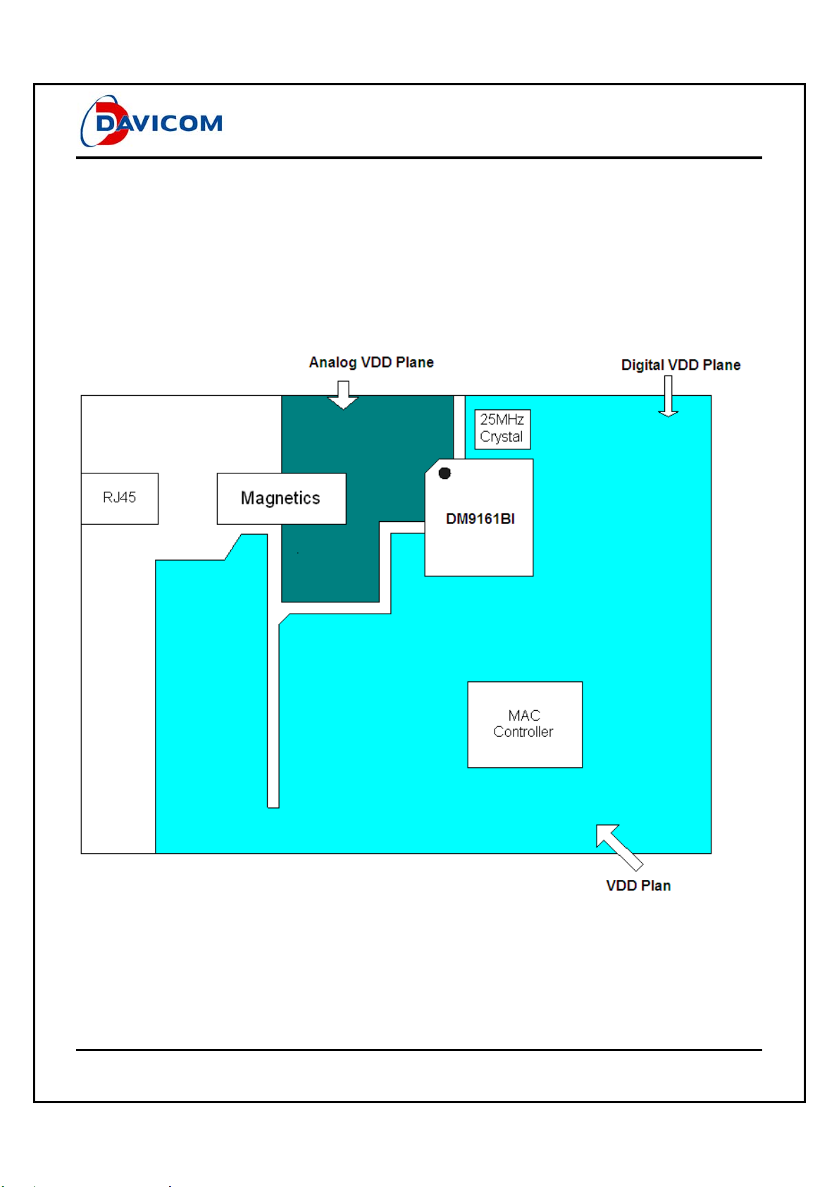
2. Power Supply Decoupling Capacitors
•Place all the decoupling capacitors for all power supply pins as close as possible to the power pads of the
DM9161BI (no more than 2.5mm from the above mentioned pins). The recommended decoupling capacitor
is 0.1µF or 0.01µF.
•The PCB layout and power supply decoupling should provide sufficient decoupling to achieve the following
when measured at the device:
(1)All DVDDs and AVDDs should be within 50m Vpp of each other,
(2)All DGNDs and AGNDs should be within 50m Vpp of each other.
(3)The resultant AC noise voltage measured across each DVDD/DGND set and AVDD/AGND set should be
less than 100m Vpp.
•The 0.1-0.01µF decoupling capacitor should be connected between each DVDD/DGND set and
AVDD/AGNDset and beplaced as close as possible to the pins of DM9161BI. The conservative approach is
to use two decoupling capacitors on each DVDD/DGND set and AVDD/AGND set. One 0.1µF is for low
frequency noise, and the other 0.01µF is for high frequency noise on the power supply.
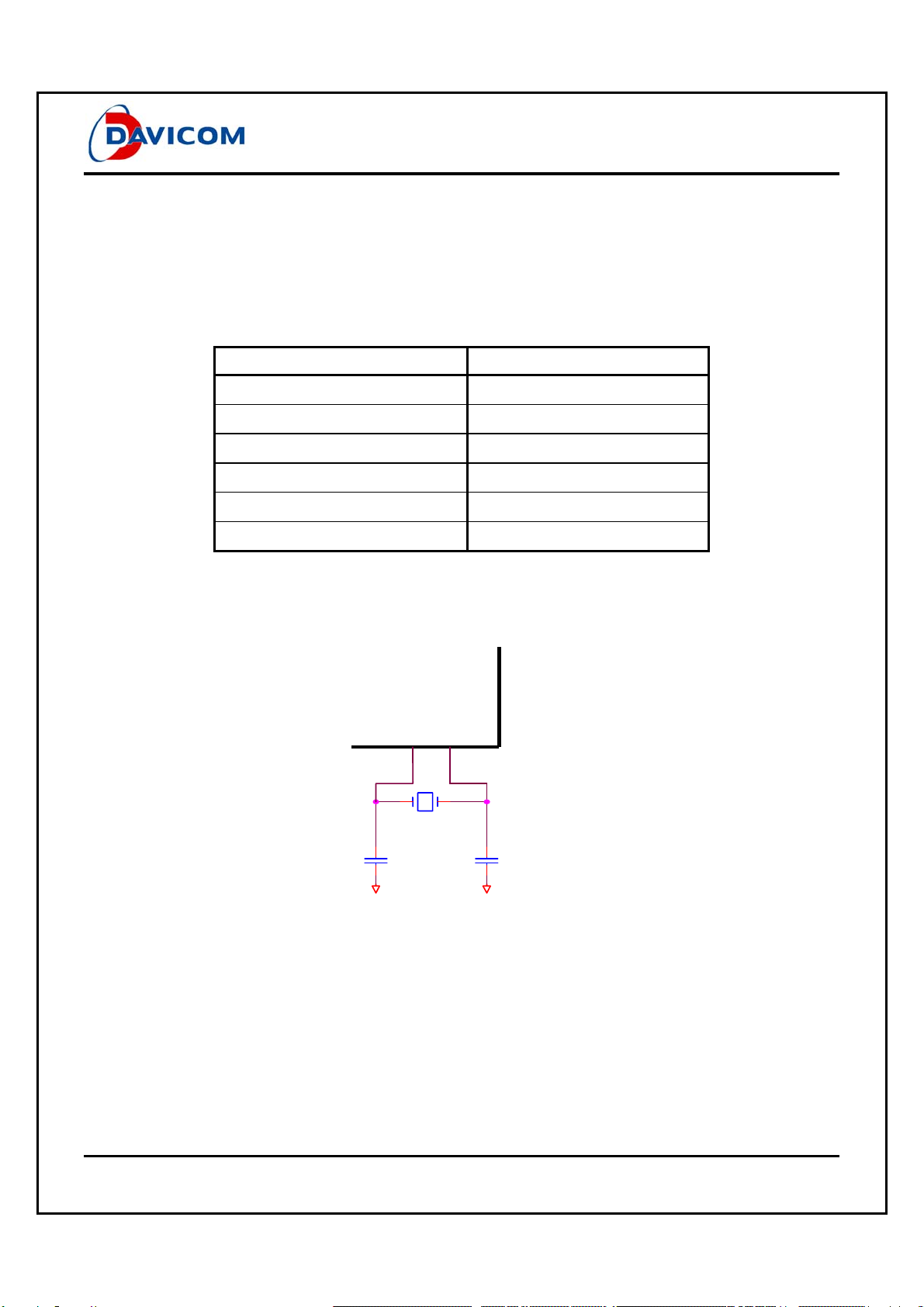
•The AVDD connection to the transmit center tap of the magnetic has to be well decoupled to minimize
common mode noise injection from the power supply into the twisted pair cable. It is recommended that a
0.01µF decoupling capacitor should be placed between the center tap AVDD to AGND ground plane. This
decoupling capacitor should be placed as close as possible to the center tap of the magnetic.10 uF or 47 uF
Capacitor should be connected between each AVDD and AGND.
Figure 2

DM9161BI
Layout Guide
6 Version: DM9161BI-LG-V10
April 10, 2008
3. Ground Plane Layout
•Place a single ground plane approach to minimize EMI. Ground plane partitioning can cause increased EMI
emissions that could make the network interface card (NIC) not comply with specific FCC part 15 and CE
regulations.
•Ground plane need separate analog ground domain and digital ground domain, the analog ground domain
and digital ground domain connected line is far away the AGND pins of DM9161BI (see Figure 4).
•All AGND pins (pin 5, 6, 46) could not directly short each other (see Figure 3-3). It must be directly connected
to analog ground domain (see Figure 3-2).
•Analog ground domain area is as large as possible
Figure 3-1
Analog ground domain
Digital ground domain
AGND
AGND
AGND
Good
Analog ground domain
Digital ground domain
AGND
AGND
AGND
Worse! AGND direct short
Figure3-2 Figure3-3

DM9161BI
Layout Guide
Version: DM9161BI-LG-V10 7
April 10, 2008
4. Power Plane Partitioning
•The power planes should be approximately illustrated in Figure 4. The ferrite bead used should have an
impedance 100Ωat 100MHz and 200mA above. A suitable bead is the Panasonic surface mound bead,
part number EXCCL4532U or an equivalent. A 10µF, 0.1µF and 0.01µF electrolytic bypass capacitors
should be connected between VDD and GND at the device side of each of the ferrite bead.
•Should separate analog power planes from noisy logic power planes.
Figure 4

DM9161BI
Layout Guide
8 Version: DM9161BI-LG-V10
April 10, 2008
5. Magnetics Selection Guide
•Refer to the following tables 5-1 and 5-2 for 10/100M magnetic sources and specification requirements. The
magnetics which meet these requirements are available from a variety of magnetic manufacturers.
Designers should test and qualify all magnetic specifications before using them in an application. The
magnetics listed in the following table are electrical equivalents, but may not be pin-to-pin equivalents.
Manufacturer Part Number
Pulse Engineering PE-68515, H1102
YCL PH163112, PH163539
Halo TG110-S050N2, TG110-LC50N2
Bel Fuse S558-5999-W2
MAGCOM HS9016, HS9024
GTS FC-618SM
Table 5-1: 10/100M Magnetics Sources
Parameter Values Units Test Condition
Tx / RX turns ratio 1:1 CT / 1:1 - -
Inductance 350
µH (Min) -
Insertion loss 1.1 dB ( Max ) 1 – 100 MHz
-18 dB ( Min ) 1 –30 MHz
-14 dB ( Min ) 30 – 60 MHz
Return loss
-12 dB ( Min ) 60 – 80 MHz
-40 dB ( Min ) 1 – 60 MHzDifferential to common
mode rejection -30 dB ( Min ) 60 – 100 MHz
Transformer isolation 1500 V -
Table 5-2: Magnetic Specification Requirements

DM9161BI
Layout Guide
Version: DM9161BI-LG-V10 9
April 10, 2008
6. Crystal Selection Guide
•A crystal can be used to generate the 25MHz reference clock instead of an oscillator. The crystal must be a
fundamental type, series-resonant, connect to XT1 and XT2, and shunt each crystal lead to ground with a
22pF capacitor as shown in Figure 6.
PARAMETER SPEC
Type Fundamental, series-resonant
Frequency 25 MHz +/- 0.01%
Equivalent Series Resistance 25 ohms max
Load Capacitance 22 pF type.
Case Capacitance 7 pF max.
Power Dissipation 1mW max.
Table 6-1: Crystal Specifications
42 43
XT1XT2
A
GND
A
GND
C18
22pf
Y1 25M
C19
22pf
Figure 6
Crystal Circuit Diagram

DM9161BI
Layout Guide
10 Version: DM9161BI-LG-V10
April 10, 2008
7. MII Signals to Mac Controller
•The length of the trace routing for the Media Independent Interface (MII) signals should be as short and direct
as possible between the DM9161BI and MAC controller (Maximum shorter than 20cm). These MII signals
are as follows,
CRS, COL, TXD3, TXD2, TXD1, TXD0, TXEN, TXCLK, TXER
RXER, RXCLK, RXDV, RXD0, RXD1, RXD2, RXD3, MDC, MDIO
•TXD [0-3] and TXCLK length mismatch does not exceed 2cm.
•RXD [0-3] and RXCLK length mismatch does not exceed 2cm.
•All signal trace should be considered to have characteristic impedance of 50 Ohm.
Table of contents
Other Davicom Transceiver manuals
Popular Transceiver manuals by other brands

SILTRONIX
SILTRONIX 1011D Installation, operation and maintanance

REXON
REXON RHP-500 Com Operation manual

Kenwood
Kenwood TH-D72A instruction manual

Midland
Midland M Zero Instruction guide

City Theatrical
City Theatrical 7400-5708 Vero Net quick start guide

Vertex Standard
Vertex Standard VXA-710 SPIRIT operating manual