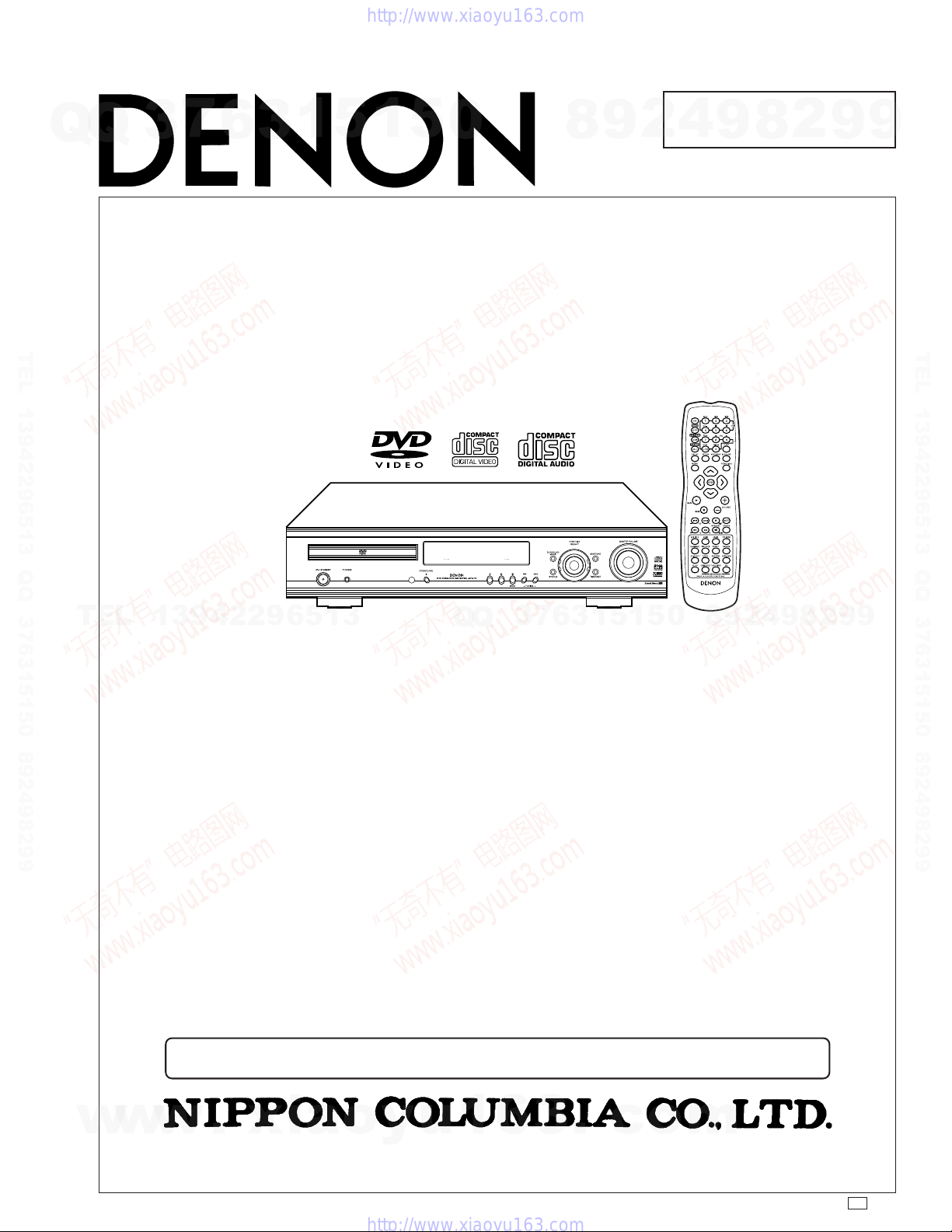
Denon ADV-700 User manual

Hi-Fi Component
SERVICE MANUAL
MODEL
ADV-700
DVD SURROUND RECEIVER
For U.S.A. , Canada &
Europe model
14-14, AKASAKA 4-CHOME, MINATO-KU, TOKYO 107-8011 JAPAN
Telephone: 03 (3584) 8111
X0115 842 NC 0108
Some illustrations using in this service manual are slightly different from the actual set.
— TABLE OF CONTENTS —
SAFETY PRECAUTIONS ................................................... 2
SPECIFICATIONS .............................................................. 2
DIAGNOSTICS OF OPTICAL PICKUP AND
REPLACING TRAVERSE UNIT ..................................... 3~5
DISASSEMBLY ............................................................. 6~10
CAUTION IN SERVICING ................................................ 10
ELECTRICAL ADJUSTMENT .......................................... 11
BLOCK DIAGRAMS .................................................... 12,13
LEVEL DIAGRAMS ..................................................... 14,15
CLOCK FLOW .................................................................. 16
SEMICONDUCTORS ................................................ 17~46
PRINTED WIRING BOARDS .................................... 47~54
NOTE FOR PARTS LIST ................................................. 55
PARTS LIST OF P.W.B. UNIT .................................. 56~71
EXPLODED VIEW ............................................................. 72
PARTS LIST OF EXPLODED VIEW ................................ 73
PARTS LIST OF DVD MECHANISM UNIT ..................... 74
EXPLODED VIEW OF DVD MECHANISM ...................... 75
POINTS OF GREASING .................................................. 76
PACKING VIEW ................................................................ 77
PACKING & ACCESSORIES ........................................... 77
WIRING DIAGRAM ........................................................... 78
MEASURING METHOD AND WAVE FORMS .......... 79,80
SCHEMATIC DIAGRAMS ......................................... 81~88
(1/8) GU-3333-1 DVD MAIN UNIT (1/2) ........................... 81
(2/8) GU-3333-1 DVD MAIN UNIT (2/2) ........................... 82
(3/8) 1U-3358-1 MAIN UNIT (1/2) .................................... 83
(4/8) 1U-3358-1 MAIN UNIT (2/2) .................................... 84
1U-3358-2 REG UNIT ............................................. 84
1U-3358-3 AUDIO REG UNIT ................................. 84
1U-3358-4 PROT/FAN UNIT .................................... 84
1U-3358-5 POSISTOR UNIT ................................... 84
1U-3358-6 D-BRIDGE UNIT .................................... 84
(5/8) 1U-3359-3 VIDEO UNIT .......................................... 85
1U-3359-5 COMPONENTUNIT ............................... 85
1U-3359-6 SCART UNIT ......................................... 85
1U-3359-7 OPT UNIT .............................................. 85
(6/8) 1U-3359-1 DISPLAY UNIT ...................................... 86
1U-3359-2 H/P UNIT ............................................... 86
1U-3359-8 SUB TRANS UNIT ................................. 86
(7/8) 1U-3360 DSP UNIT (1/2) ..................................... 87
(8/8) 1U-3360 DSP UNIT (2/2) ..................................... 88
w
w
w
.
x
i
a
o
y
u
1
6
3
.
c
o
m
Q
Q
3
7
6
3
1
5
1
5
0
9
9
2
8
9
4
2
9
8
T
E
L
1
3
9
4
2
2
9
6
5
1
3
9
9
2
8
9
4
2
9
8
0
5
1
5
1
3
6
7
3
Q
Q
TEL 13942296513 QQ 376315150 892498299
http://www.xiaoyu163.com

ADV-700
2
SPECIFICATIONS
Audio section
• Power amplifier
Output power: Front: 35 W + 35 W (6 Ω/ohms, 1 kHz with 10% T.H.D.)
Center: 35 W + 35 W (6 Ω/ohms, 1 kHz with 10% T.H.D.)
Surround: 35 W + 35 W (6 Ω/ohms, 1 kHz with 10% T.H.D.)
Output terminals: Front, Center, Surrond: 6 ~16 Ω/ohms
• Analog
Input sensitivity / input impedance: 200 mV / 47 kΩ/kohms
Frequency response: 10 Hz ~ 70 kHz: +0.3 dB (DIRECT mode)
S / N : 98 dB (DIRECT mode)
Rated output: 1.2 V (Subwoofer preout, 20 Hz)
• Digital
Digital input / output: Format Digital audio interface
Video secion
• Standard video jacks
Input / output level and inpedance: 1 Vp-p, 75 Ω/ohms
• S-video jacks
Input / output level and inpedance: Y (brightness) signal 1 Vp-p, 75 Ω/ohms
C (color) signal 0.286 Vp-p, 75 Ω/ohms (U.S.A. & Canada model)
C (color) signal 0.3 Vp-p, 75 Ω/ohms (Europe model)
• Color cimponent video jacks (DVD output) (U.S.A. & Canada model)
Input / output level and inpedance: Y (brightness) signal 1 Vp-p, 75 Ω/ohms
CB(blue) signal 0.648 Vp-p, 75 Ω/ohms
CR(red) signal 0.648 Vp-p, 75 Ω/ohms
• AV1 connector (Europe model)
Video output: 1Vp-p, 75Ω/ohms
S-video output: Y (brightness) signal 1 Vp-p, 75 Ω/ohms
C (color) signal 0.3 Vp-p, 75 Ω/ohms
RGB output (DVD only): R/G/B signal 0.7 Vp-p, 75 Ω/ohms
Audio output: L/R (Fixed output)
Tuner section
[FM] (note: µV at 75 Ω/ohms, 0 dBf=1×10-15 W) [AM]
Receiving Range
U.S.A. & Canada model: 87.50 MHz~107.90 MHz 520 MHz~1710 MHz
Europe model: 87.50 MHz~108.00 MHz 522 MHz~1611 MHz
Usable Sensitivity: 1.5 µV (14.8 dBf)
DVD section
Signal Format: NTSC/PAL
Applicable discs: (1) DVD-Video discs
1-layer 12 cm single-sided discs, 2-layer 12 cm single-sided
discs, 2-layer 12cm double-sided discs (1 layer per side)
1-layer 8 cm single-sided discs, 2-layer 8 cm single-sided
discs, 2-layer 8 cm double-sided discs (1 layer per side)
(2) Compact discs (CD-DA, Video CD)
12 cm discs, 8 cm discs
Audio output: Fixed output level: 2 Vrms, (CDR/TYPE, VCR OUT)
Clock,Timer section
Clock system: Power source synchronous system
Timer functions: Everyday timer (DVD or Tuner): 1 setting
Sleep timer: maximum 120 min.
General
Power Supply: AC 120 V, 60 Hz (For U.S.A. & Canada model)
AC 230 V, 50 Hz (For Europe model)
Power Consumption: 135 W (Standby 1.2 W) (For U.S.A. & Canada model)
145 W (Standby 1.2 W) (For Europe model)
Maximuim external
Dimensions: 434(W) ×90 (H) ×415 (D) mm (17.1” ×3.5” ×16.3”)
Mass: 9.4 kg (20.7 lbs)
Remote Control Unit RC-902 (For U.S.A. & Canada model)
RC-901 (For Europe model)
Type: Infrared pulse
Power Supply: DC 3V, 2 “AA/R6P” batteries
SAFETY PRECAUTIONS
The following check should be performed for the continued protection of the customer and service technician.
LEAKAGE CURRENT CHECK
Before returning the unit to the customer, make sure you make either (1) a leakage current check or (2) a line to
chassis resistance check. If the leakage current exceeds 0.5 milliamps, or if the resistance from chassis to either
side of the power cord is less than 460 kohms, the unit is defective.
This product incorporates copyright protection technology that is protected by method claims of certain U.S. patents and other intellectual property rights
owned by Macrovision Corporation and other rights owners. Use of this copyright portection technology must be authorized by Macrovision Corporation,
and is intended for home and other limited viewing uses only unless otherwise authorized by Macrovision Corporation. Reverse engineering or
disassembly is prohibited.
∗Design and specifications are subject to change without notice in the course of porduct improvement.
w
w
w
.
x
i
a
o
y
u
1
6
3
.
c
o
m
Q
Q
3
7
6
3
1
5
1
5
0
9
9
2
8
9
4
2
9
8
T
E
L
1
3
9
4
2
2
9
6
5
1
3
9
9
2
8
9
4
2
9
8
0
5
1
5
1
3
6
7
3
Q
Q
TEL 13942296513 QQ 376315150 892498299
http://www.xiaoyu163.com

ADV-700
3
DIAGNOSTICS OF OPTICAL PICKUP AND REPLACING TRAVERSE UNIT
Make failure diagnostics of the Optical Pickup as follows.
If the laser drive current becomes more than 1.5 times of the initial value, the Optical Pickup should be replaced.
The laser drive current is registered on the seal attached to the rear of the Mecha. Unit.
In case of replacing the Pickup, change the whole part of the Traverse Unit.
No mechanical adjustment is necessary after the replacement.
Disc no read,
unsteady playback, etc.
Laser drive current check
HF wave form check
(Refer to page 79, 80)
Present value exceeds
the initial value by 1.5 times
Traverse Unit replacing
(See page 9 for details)
Laser current registering
after replacement
Step: Disc playback
Write the measured value
on the seal attached to the Mecha. Unit
* As to the measuring method, refer to page 4
Label Indication of DVD Mechanism
Laser current consumption value
ex) DVD ***mA, CD ***mA
Example:
DVD 30mA
CD 30mA
w
w
w
.
x
i
a
o
y
u
1
6
3
.
c
o
m
Q
Q
3
7
6
3
1
5
1
5
0
9
9
2
8
9
4
2
9
8
T
E
L
1
3
9
4
2
2
9
6
5
1
3
9
9
2
8
9
4
2
9
8
0
5
1
5
1
3
6
7
3
Q
Q
TEL 13942296513 QQ 376315150 892498299
http://www.xiaoyu163.com

ADV-700
4
Note for Handling the Laser Pick-up
The protection for the damage of laser diode.
If you want to change the optical device unit from any other units, you must keep the following.
(1) It should be done at the desk already took measures the static electricity in care of removing the OPU's
(Optical device unit) connector cable.
(2) Workers should be put on the "Earth Band".
(3) It shold be done to add the solder to the short land to prevent the broken Laser diode before removing the
24P FFC cable.
(4) Don't touch OPU's connector parts carelessly.
Replacement of the Laser Pick-up (Traverse Unit)
Check the Iop (Laser drive current).
If the present Iop (current) value exceeds +50% of the initial value, replace the Traverse unit (Laser Pick-up) with a new
one.
LD2
LD1LD3LD4
When measureing Laser drive current (Iop), playback the discs (CD, DVD) described below, measure Iop for CD Laser and
DVD Laser by the test point (LD1 ~ LD4) on the DVD Main P.W.B.
Test Disc : DVD/DVDT-S01 or commercially available discs.
: CD/TCD-784 (manufactured by ALMEDIO INC) or commercially available discs.
Iop Measurement Method
DVD Main Unit foil side
LD2
LD1
1. DVD Laser current measurement
(1) Connect the oscilloscope to LD1 of test point
for GND side and LD2 of test point for signal
side.
(2) Playback the title 1 / chapter 1 of the DVD
Test Disc.
(3) Measure the voltage between LD1 and LD2,
calculate Iop by the formula as shown below.
Iop= Measurement Voltage Value
39 (Resistance Value)
2. CD Laser current measurement
(1) Connect the oscilloscope to LD3 of test point
for GND side and LD4 of test point for signal
side.
(2) Playback the track 1 of the CD Test Disc.
(3) Measure the voltage between LD3 and LD4,
calculate Iop by the formula as shown below.
Iop= Measurement Voltage Value
39 (Resistance Value)
w
w
w
.
x
i
a
o
y
u
1
6
3
.
c
o
m
Q
Q
3
7
6
3
1
5
1
5
0
9
9
2
8
9
4
2
9
8
T
E
L
1
3
9
4
2
2
9
6
5
1
3
9
9
2
8
9
4
2
9
8
0
5
1
5
1
3
6
7
3
Q
Q
TEL 13942296513 QQ 376315150 892498299
http://www.xiaoyu163.com

ADV-700
5
Optical Pick-up Diagnostics and Replacement
When repairing, carry out failure diagnostics by following the procedure described below.
If the present value of the laser drive current is 50% up to initial value, it is the point of the pickup replacement.
In case of the pickup replacement, replace the Traverse Unit with no adjustment.
The initial value is indicated on the label on back side of Mecha.
NO DISC indicated, Playback not smooth, etc.
Laser drive current check
HF signal check
Traverse Unit replacement (refer to page 9)
Present value: 50% up to initial value
Laser drive current check after replacement.
If the present value is less than 80mA, write on
the new label by hand, put on the new label over
the old label.
If the present value exceeds 80mA,
replace the Traverse Unit with a new one.
Cause: Damaged electrostatically when replaced.
w
w
w
.
x
i
a
o
y
u
1
6
3
.
c
o
m
Q
Q
3
7
6
3
1
5
1
5
0
9
9
2
8
9
4
2
9
8
T
E
L
1
3
9
4
2
2
9
6
5
1
3
9
9
2
8
9
4
2
9
8
0
5
1
5
1
3
6
7
3
Q
Q
TEL 13942296513 QQ 376315150 892498299
http://www.xiaoyu163.com

ADV-700
6
DISASSEMBLY
( Follow the procedure below in reverse order when reassembling )
1. Top Cover
1) Remove 4 screws
1
on both sides.
2) Remove 6 screws 2on the rear panel.
3) Detach the Cover as shown in the arrow
direction.
2. Front Panel
1) Remove 4 screws 3from the bottom edge of the
Front Panel.
2) Disconnect FFC, 3P Connector, and 5P Connector
from the Main PWB.
3) Detach the Front Panel together with the Inner
Panel as shown in the arrow direction.
1
1
1
1
2
2
2
3
3
3
3
MAIN P.W.B.
3P Connector
5P Connector
Front Panel
FFC
Inner Panel
w
w
w
.
x
i
a
o
y
u
1
6
3
.
c
o
m
Q
Q
3
7
6
3
1
5
1
5
0
9
9
2
8
9
4
2
9
8
T
E
L
1
3
9
4
2
2
9
6
5
1
3
9
9
2
8
9
4
2
9
8
0
5
1
5
1
3
6
7
3
Q
Q
TEL 13942296513 QQ 376315150 892498299
http://www.xiaoyu163.com

ADV-700
7
5. Rear Panel
1) Remove the Cord Bush.
2) Remove 5 screws 6, 20 screws
7
, and 3 screws
8
on the Rear Panel.
4. DVD Mecha. Unit
1) Remove 4 screws 5on the DVD Mecha. Unit.
2) Disconnect FFC x 2, 14P Connector, and 9P
Connector from the DVD Mecha. Unit.
3. DSP PWB
1) Remove 4 screws
4
fixing the DSP PWB.
2) Disconnect FFC x 3 from the DSP PWB.
4
4
44
FFC
DSP P.W.B.
514P Connector
9P Connector
FFC
FFC
Cord Bush
6
7
8
67
6
7
6
w
w
w
.
x
i
a
o
y
u
1
6
3
.
c
o
m
Q
Q
3
7
6
3
1
5
1
5
0
9
9
2
8
9
4
2
9
8
T
E
L
1
3
9
4
2
2
9
6
5
1
3
9
9
2
8
9
4
2
9
8
0
5
1
5
1
3
6
7
3
Q
Q
TEL 13942296513 QQ 376315150 892498299
http://www.xiaoyu163.com

ADV-700
8
6. Video PWB
1) Disconnect FFC x 2, 11P Connector, and 3P
Connector from the Video PWB.
2) Detach the Video PWB from the PWB Holder.
7. Main PWB
1) Remove 5 screws 9and 1 screw 10 on the Main
PWB.
2) Remove 6 screws
11
from the bottom of the
Chassis.
3) Disconnect 8P, 4P x 2, and 3P Connector from the
Main PWB.
FFC
3P Connector
FFC
11P Connector
(Europe Model)
P.W.B. Holder
Video P.W.B.
9
10
10P Connector
(USA, Canada Model)
Main P.W.B
4P 3P
9
11
8P Connector
w
w
w
.
x
i
a
o
y
u
1
6
3
.
c
o
m
Q
Q
3
7
6
3
1
5
1
5
0
9
9
2
8
9
4
2
9
8
T
E
L
1
3
9
4
2
2
9
6
5
1
3
9
9
2
8
9
4
2
9
8
0
5
1
5
1
3
6
7
3
Q
Q
TEL 13942296513 QQ 376315150 892498299
http://www.xiaoyu163.com

ADV-700
9
1
TRAVERSE UNIT DISASSEMBLY
(Follow the procedure below in reverse order when reassembling)
Caution: The optical pickup can be damaged easily by static electricity charged on human body. Take necessary anti-static
measures when repairing around the optical pickup.
1. Guide Clamp Bracket disassembly
(1) Remove 2 screws 1.
(2) Remove Guide Clamp Bracket to arrow direction.
2. Tray disassembly
(1) Remove to arrow direction.
(2) Solder the short-circuit (see in the frame).
Guide Clamp Bracket
Tray
Solder to Short-Circuit (DVD)
Solder to Short-Circuit (CD)
w
w
w
.
x
i
a
o
y
u
1
6
3
.
c
o
m
Q
Q
3
7
6
3
1
5
1
5
0
9
9
2
8
9
4
2
9
8
T
E
L
1
3
9
4
2
2
9
6
5
1
3
9
9
2
8
9
4
2
9
8
0
5
1
5
1
3
6
7
3
Q
Q
TEL 13942296513 QQ 376315150 892498299
http://www.xiaoyu163.com

ADV-700
10
CAUTION IN SERVICING
Initialization
Initialization should be performed when the µcom, peripheral parts of µcom, and DVD Main P.W.B. are replaced.
How to initialize
At the player is in the state of AC OFF, turn the AC ON with pressing the PLAY ( ) and STOP ( ) buttons simultaneously.
Check that the Standby LED lights orange and the initialization has been activated. (until "INITIALIZE" disappears from
the FL display).
Note: All user settings will be lost and its factory setting will be recovered when this initialization is made. So make sure to
memorize your setting for restoring after the initialization.
Note for disassembly Traverse Unit
(1) When assembling, reverse the order of the above.
(2) When inserting Tray, confirm boss on Slide Cam set
to ditch of the Tray (Compare with right drawing).
Slide gear
Tray
Boss
24P FFC (CX241)
3P PH WIRE (CX031)
Damper
15P FFC (CX151)
2
3. Traverse Unit disassembly
(1) Remove 24P FFC (CX241), 15P FFC (CX151),
5P PH WIRE (CX051) and 3P PH WIRE (CX031)
connecting with from the DVD Main P.W.B.
(2) Remove 4 screws of 2fixing Damper.
(3) Remove Traverse Unit to arrow direction.
DVD Main P.W.B.
w
w
w
.
x
i
a
o
y
u
1
6
3
.
c
o
m
Q
Q
3
7
6
3
1
5
1
5
0
9
9
2
8
9
4
2
9
8
T
E
L
1
3
9
4
2
2
9
6
5
1
3
9
9
2
8
9
4
2
9
8
0
5
1
5
1
3
6
7
3
Q
Q
TEL 13942296513 QQ 376315150 892498299
http://www.xiaoyu163.com

ADV-700
11
Luminance Signal Output
Measurement Point Adjustment Point Mode Disc
Video Output Pin Terminal VR701 Color Bar 75% T12 Playback DVD T -S01
Measuring Device: Oscilloscope 200 mV/div, 10 Ps/div
Adjustment Value: 1000 mVp-p r20 mV
1. Video Output (Interlace) Adjustment
For compatibility of video signal output.
1. Connect the monitor TV to the video output terminal and terminate at 75 Ohms.
2. Play back the color bar part Title 12 of the DVD Test Disc.
3. Adjust the VR701 so that the luminance signal (Y+S) output is as shown below.
Adjustment Value = 1000 mVp-p ±±
±±
±20 mV
1000mV
20mV
2. Video Output (Interlace) Adjustment
Note: CB Output should be 75 Ωterminal
For compatibility of video signal output.
1. Connect the oscilloscope to CB output Pin terminal for CH-1 and CR output Pin terminal for CH-2. (Trigger)
2. Playback the color bar part title 12 of the DVD Test Disc.
3. Adjust the VR702 so that the CB signal output is as shown below.
Measurement Point Adjustment Point Mode Disc
CBOutput Pin terminal VR702 Color Bar 75% T12 Playback DVDT-SO1
Measuring Device: Oscilloscope 100 mV/div, 10 Ps/div
Adjustment Value: *525 mVp-p r11 mV Europe/Asia models
Adjustment Value = *525 mVp-p ±±
±±
±11mV
CB Signal Output
*: 486 mVp-p ±±
±±
±11mV for U.S.A. & Canada model
*
525mV*
11mV
ELECTRICAL ADJUSTMENT
The following adjustment is electrical adjustments. These adjustments are to be performed after replacing the printed circuit
boards.
w
w
w
.
x
i
a
o
y
u
1
6
3
.
c
o
m
Q
Q
3
7
6
3
1
5
1
5
0
9
9
2
8
9
4
2
9
8
T
E
L
1
3
9
4
2
2
9
6
5
1
3
9
9
2
8
9
4
2
9
8
0
5
1
5
1
3
6
7
3
Q
Q
TEL 13942296513 QQ 376315150 892498299
http://www.xiaoyu163.com

DVD DRIVE
MECHA
UNIT
FRONTEND
PROCESSOR
[TA1293F]
4ch MOTOR
DRIVER
[BA5952FP]
SPINDLE
MOTOR
DRIVER
[AN8471]
4M DRAM 4M DRAM
DISC SERVO
PROCESSOR
[TC9453F]
ATAPI
INTERFACE
DVD DECODER
[TC9469BF]
DRIVE
CONTROL
m
-COM
[TMP95CW64F]
MAIN
UNIT
MAIN UNIT
1U-3358-1
1U-3358-1
+3.7V REG.
+3.3V[D1]REG.
[TC7WT125]
DVD PROCESSOR
[ES4408]
16M SDRAM x2
8M FLASH ROM
[HY29F080T]
E2PROM
[S24C01A] I/O EXPANDER
[HCT273]
27MHz
OSC
BUFFER
AMP
VIDEO ENCODER
[ADV7172]
24P FFC
15P FFC
5P PH
3P PH
+5V[USW]
+5V[V]
+5V[D1]
GND[D1]
GND[V]
GND[A]
+12V[M]
+5V[D2]
GND[D2]
96k,DEEM,/DFRES
TSDO,TWS,TBCK,MCLK
SPDIF
PROG/INT
/RST
YVU0~7
27M
HSYNC,VSYNC
SDA,SCL
VIDCNTL1,2,RGB-H
+5V[V]
G/Y
B/Cb
R/Cr
Y
C
HSYNC
VSYNC
8
LD8~15
/RST
HRESET
DMO,TRD
DMO
DATA
CS,CLK
ON/ST
PDET
(+5V[D])
/DFRES
/RST
/RST
I C BUS
2
DVD MAIN UNIT GU-3333
VIDEO PWB UNIT
1U-3359-3
DSP PWB UNIT
1U-3360
ADV-700 BLOCK DIAGRAM (1/2)
(Mechanism section)
8
76
5
4
3
2
1
A
B
C
D
E
ADV-700
12
BLOCK DIAGRAMS
w
w
w
.
x
i
a
o
y
u
1
6
3
.
c
o
m
Q
Q
3
7
6
3
1
5
1
5
0
9
9
2
8
9
4
2
9
8
T
E
L
1
3
9
4
2
2
9
6
5
1
3
9
9
2
8
9
4
2
9
8
0
5
1
5
1
3
6
7
3
Q
Q
TEL 13942296513 QQ 376315150 892498299
http://www.xiaoyu163.com

(E2 ONLY)
BA7660(Europe model only)
BA4053(E2 ONLY)
DVD MECHA FRONT-END CIRCUIT
FL TUBE
ES4408
15-ST-36GN ML6427
DVD DSP
BA7660(Europe model only)
DVD DECODER VIDEO FILTER Cr
Cb Y
YVCR IN
FL DRIVER YC
M66005FP
CY
CPU VTV/DBS IN
C
Y
V.AUX IN
C
KEY
ROTARY ENCODER ROM
CPU
M30624FGGP
RAM
(DOWN MIX)
REMOCON
BA7625
Y
RPM6938-V4
MONITOR OUT
C
Y
VCR OUT
C
BA7626
VCR IN
TV/DBS IN
RDS
(E2/E3 ONLY) TUNER PACK
LC72720NM
V.AUX IN
(Europe model only)
BA7625
MONITOR OUT
VCR OUT
ROM
2Mbit
RELAY
PIC-212DM
OPT OUT DIR AUDIO DSP
LC89055W CS49392
H/P
OPT IN 1
OPT IN 2 SWITCHING POWER AMP
BA15218 BA15218 BA15218 LC4966 BA15218 STK402-050
BA15218 BA15218
VCR IN
TV/DBS IN
V.AUX IN
CDR/TAPE IN
STK402-250
SUBWOOFER
TUNER IN FUNCTION
(J ONLY)
TC9164AN
CODEC
AK4527
VOLUME
DAC M62446FP
AD1854KRSRL
VCR OUT
CDR/TAPE OUT
MUTE
MUTE
MUTE
MUTE
MUTE
MUTE
MUTE
MUTE
MUTE
MUTE
MUTE
MUTE
FRONT L
FRONT R
SURR L
SURR L
CENTER
A/D CONVERTER
6ch D/A CONVERTER
MUTE
MUTE
MUTE
PREOUT
COMPOSITE VIDEO S-VIDEO COMPONENT VIDEO
DIGITAL IN/OUT
AUDIO IN/OUT
SPEAKER OUT
SDB
SDB
MUTE
MUTE
MUTE
Europe model:SCART TERMINAL
USA,Canada model:3P PINJACK
C
V
Y
Y
V
C
A
A
1U-3359-1
1U-3359-7 1U-3360
1U-3358-1
1U-3359-3
1U-3359-2
UADV-7 (DVD ENGINE )
1U-3359-5,6
ADV-700 BLOCK DIAGRAM (2/2)
8
76
5
4
3
2
1
A
B
C
D
E
ADV-700
13
w
w
w
.
x
i
a
o
y
u
1
6
3
.
c
o
m
Q
Q
3
7
6
3
1
5
1
5
0
9
9
2
8
9
4
2
9
8
T
E
L
1
3
9
4
2
2
9
6
5
1
3
9
9
2
8
9
4
2
9
8
0
5
1
5
1
3
6
7
3
Q
Q
TEL 13942296513 QQ 376315150 892498299
http://www.xiaoyu163.com

+
− −
+
− −
+
+ +
MUT-
ING
ATT
FRONT
SP OUT
MUT-
ING
D/A
DSP
A/D
CD IN
config1:OFF
config2:ON
M62446 (1/3)
H/P OUT
BUFF.
AMP
POWER
AMP
E.VOL
TONE
TONE
REV.
AMP
D/A OUT
L.P.F.
A/D IN
REV. AMP
A/D IN
REV. AMP
FROM SWch
other ch
PRE.
AMP
STEREO
H.P.F.
INPUT
BUFF.AMP
SW
MIX AMP
fc=80Hz.12dB/OCT
++ +
MUT-
ING
CENTER
SURROUND
SP OUT
MUT-
ING
D/A
M62446 (2/3)
BUFF.
AMP
POWER
AMP
E.VOL
FROM
DSP
PRE.
AMP
D/A OUT
L.P.F.
(dB)
30
20
10
(200mV) 0
-10
-20
CD IN
-11.5dB
A/D
0dBPS
-10dBPS
-20dBPS
-30dBPS
D/A
0dBFS
-10dBFS
-20dBFS
(106mV)
6dB
Other than PROLOGIC
PROLOGIC -15dB
-18dB
6.3dB
30.1dB
SP OUT
1.66V
(0.35W/8Ω)
-30dBFS
D/A
0dBFS
-10dBFS
-20dBFS
(106mV)
6dB
Other than PROLOGIC
PROLOGIC -15dB
-18dB
6.9dB
30.1dB
SP OUT
1.66V
(0.35W/8Ω)
-30dBFS
FRONT
CENTER
SURROUND
8
76
5
4
3
2
1
A
B
C
D
E
ADV-700
14
LEVEL DIAGRAMS
w
w
w
.
x
i
a
o
y
u
1
6
3
.
c
o
m
Q
Q
3
7
6
3
1
5
1
5
0
9
9
2
8
9
4
2
9
8
T
E
L
1
3
9
4
2
2
9
6
5
1
3
9
9
2
8
9
4
2
9
8
0
5
1
5
1
3
6
7
3
Q
Q
TEL 13942296513 QQ 376315150 892498299
http://www.xiaoyu163.com

+
− −
+
MUT-
ING
SW
PREOUT
MUT-
ING
D/A
M62446 (3/3)
BUFF.
AMP
E.VOL
D/A OUT
L.P.F.
PRE.
AMP
FROM
DSP
D/A
0dBFS
-10dBFS
-20dBFS
-30dBFS 6dB
-18dB
Subwoofer
PREOUT
75mV
LINE
AMP
LINE
AMP
-40dBFS
-35dBFS
18.6dB
2.9dB 3.3dB
7.5dB
To FRONT ch
Config-2
Config-1
SUBWOOFER
8
76
5
4
3
2
1
A
B
C
D
E
ADV-700
15
w
w
w
.
x
i
a
o
y
u
1
6
3
.
c
o
m
Q
Q
3
7
6
3
1
5
1
5
0
9
9
2
8
9
4
2
9
8
T
E
L
1
3
9
4
2
2
9
6
5
1
3
9
9
2
8
9
4
2
9
8
0
5
1
5
1
3
6
7
3
Q
Q
TEL 13942296513 QQ 376315150 892498299
http://www.xiaoyu163.com

DIR DSP CODEC
IC107 IC109 IC108
LC89055W
CS49329 AK4527VQ
SN74LV244A
CKOUT(13) MCLK(44)
BCK(14) (25)SCLKN1,(28)CMPCLK SCLK(43)
LRCK(15) (26)LRCLKN1,(29)CMPREQ LRCLK(42)
DATAO(16) (22)SDATAN1 AUDATA0(41) (6)SDTI1
(27)CMPDAT AUDATA1(40) (7)SDTI2
XMCK(20) AUDATA2(39) (8)SDTI3
X'TAL
(39)MCLK
(4)BICK
DIR IN A/D IN (5)LRCK
SW1 ON OFF
SW2 ON OFF (9)SDTO
SW3 ON OFF
SW4 OFF ON (10)
SW5 OFF ON /CK Q2(7)
SW6 OFF ON
IC114 Q8(13)
SN74LV4040APW
BINARY COUNTER
A/D SWitch
SN74HC244
IC113
SN74HC244
(17) SW1
(13) SW3
(15) SW2
( 2) SW4
( 4) SW5
( 6) SW6
(16)
(14)
(3)
(5)
(7)
(18)
8
76
5
4
3
2
1
A
B
C
D
E
ADV-700
16
CLOCK FLOW
w
w
w
.
x
i
a
o
y
u
1
6
3
.
c
o
m
Q
Q
3
7
6
3
1
5
1
5
0
9
9
2
8
9
4
2
9
8
T
E
L
1
3
9
4
2
2
9
6
5
1
3
9
9
2
8
9
4
2
9
8
0
5
1
5
1
3
6
7
3
Q
Q
TEL 13942296513 QQ 376315150 892498299
http://www.xiaoyu163.com

ADV-700
17
1 P94 E2P CS Chip select signal to EEPROM
2 P93 62446 LATCH Serial data latch to E. VR IC
3 P92 62446 DATA, E2P DI, FUNC DA Serial data to EEPROM/E. VR IC/Input Switch IC
4 P91 E2P DO Serial data from EEPROM
5 P90 62446 CLK, E2P SK, FUNC CLK Serial clock to EEPROM/E. VR IC/Input Switching IC
6 BYTE (VSS) GND
7 CNVSS (PullDown), FLASH CNVss Flash write mode select input
8 P87 BUS ON/OFF Serial data/clock separate command output to E. VR IC
9 P86 FUNC CE(STB) Data latch to Input Switch IC
10 RESET RESET Reset input
11 XOUT XTAL(12.5MHz) Oscillator output (12.5 MHz)
12 VSS (VSS) GND
13 XIN XTAL(12.5MHz) Oscillator input (12.5 MHz)
14 VCC (VCC) Power supply
15 P85 (PullUp) NMI, not used
16 P84 PROTECT Speaker and Drive IC abnormal detect
17 P83 /CS Comm. chip select input with DVD
P1
2
/D
10
76
P1
2
/D
9
77
P1
0
/D
8
78
P0
7
/D
7
79
P0
6
/D
6
80
P0
5
/D
5
81
P0
4
/D
4
82
P0
3
/D
3
83
P0
2
/D
2
84
P0
1
/D
1
85
P0
0
/D
0
86
P10
7
/AN
7
/KI
3
87
P10
6
/AN
6
/KI
2
88
P10
5
/AN
5
/KI
1
89
P10
4
/AN
4
/KI
0
90
P10
3
/AN
3
91
P10
2
/AN
2
92
P10
1
/AN
1
93
AV
SS
94
P10
0
/AN
0
95
V
REF
96
AV
CC
97
P9
7
/AD
TRG
/S
IN
498
P9
6
/ANEX1/S
OUT
499
P9
5
/ANEX0/SLK4 100
P4
2
/A
18
50
P4
3
/A
19
49
P4
4
/CS0
48
P4
5
/CS1
47
P4
6
/CS2
46
P4
7
/CS3
45
P5
0
/WRL/WR
44
P5
1
/WRH/BHE
43
P5
2
/RD
42
P5
3
/BCLK
41
P5
4
/HLDA
40
P5
5
/HOLD
39
P5
6
/ALE
38
P5
7
/RDY/CLK
OUT
37
P6
0
/CTS
0
/RTS
0
36
P6
1
/CLK
0
35
P6
2
/RXD
0
34
P6
3
/TXD
0
33
P6
4
/CTS
1
/RTS
1
/CTS
0
/CLKS
1
32
P6
5
/CLK
1
31
P6
6
/RXD
1
30
P6
7
/TXD
1
29
P7
0
/RXD
2
/SDA/TA0
OUT
28
P7
1
/RXD
2
/SCL/TA0
IN
/TB5
IN
27
P7
2
/CLK
2
/TA1
OUT
/V
26
P1
3
/D
11
75
P1
4
/D
12
74
P1
5
/D
13
/INT
3
73
P1
6
/D
14
/INT
4
72
P1
7
/D
15
/INT
5
71
P2
0
/A
0
(/D
0
/-)
70
P2
1
/A
1
(/D
1
/D
0
)
69
P2
2
/A
2
(/D
2
/D
1
)
68
P2
3
/A
3
(/D
3
/D
2
)
67
P2
4
/A
4
(/D
4
/D
3
)
66
P2
5
/A
5
(/D
5
/D
4
)
65
P2
6
/A
6
(/D
6
/D
5
)
64
P2
7
/A
7
(/D
7
/D
6
)
63
V
SS
62
P3
0
/A
8
(/-/D
7
)
61
V
CC
60
P3
1
/A
9
59
P3
2
/A
10
58
P3
3
/A
11
57
P3
4
/A
12
56
P3
5
/A
13
55
P3
6
/A
14
54
P3
7
/A
15
53
P4
0
/A
16
52
P4
1
/A
17
51
P9
4
/DA
1
/TB4
IN
1
P9
3
/DA
0
/TB3
IN
2
P9
4
/TB2
IN
/S
OUT
33
P9
1
/TB1
IN
/S
IN
34
P9
0
/TB0
IN
/CLK3 5
BYTE 6
CNV
SS
7
P8
7
/X
CIN
8
P8
6
/X
COUT
9
RESET 10
X
OUT
11
V
SS
12
X
IN
13
V
CC
14
P8
5
/NMI 15
P8
4
/INT
2
16
P8
3
/INT
1
17
P8
2
/INT
0
18
P8
1
/TA4
IN
/U 19
P8
0
/TA4
out
/U 20
P7
7
/TA3
IN
21
P7
6
/TA3
OUT
22
P7
5
/TA2
IN
/W 23
P7
4
/TA2
out
/W 24
P
7
3
/CTS
2
/RTS
2
/TA1
IN
/V 25
M30624FG Terminal Function
SEMICONDUCTORS
M30624FG (MA: IC101)
IC's
Note: Abbreviation ahead of IC No. indicates the name of P.W.B.
DVD: DVD Main P.W.B.
MA: Main P.W.B.
D/V: Display / Video P.W.B.
DS: DSP P.W.B.
Port Name Function
Pin
No. Symbol
w
w
w
.
x
i
a
o
y
u
1
6
3
.
c
o
m
Q
Q
3
7
6
3
1
5
1
5
0
9
9
2
8
9
4
2
9
8
T
E
L
1
3
9
4
2
2
9
6
5
1
3
9
9
2
8
9
4
2
9
8
0
5
1
5
1
3
6
7
3
Q
Q
TEL 13942296513 QQ 376315150 892498299
http://www.xiaoyu163.com

ADV-700
18
18 P82 RESERVED(DENON BUS) Arbitration input on DENON BUS (same as serial data)
19 P81 50/60 Detect input of power pulse (50/60 Hz)
20 P80 FAN ON/OFF Fan motor drive output
21 P77 IN JOGB JOG pulse input B for function switching
22 P76 IN JOGA JOG pulse input A for function switching
23 P75 VOL JOGB JOG pulse input B for VOL
24 P74 VOL JOGA JOG pulse input A for VOL
25 P73 FLCS Chip select output to FL Driver IC
26 P72 RESERVED(DENON BUS) Serial sync clock output on DENON BUS
27 P71 RESERVED(DENON BUS) Serial data input on DENON BUS
28 P70 RESERVED(DENON BUS) Serial data output on DENON BUS
29 P67 FLDA, FLASH TxD Serial data output to FL Driver IC
30 P66 PULL DOWN, FLASH RxD Open pin, serial data input at flash write
31 P65 FLCK, FALSH MODE, FLASH CLK Serial clock output to FL Driver IC
32 P64 FL RESET, FLASH BUSY Reset output to FL Driver IC
33 P63 sDATAout(DVD) Serial comm. output with DVD
34 P62 sDATAin(DVD) Serial comm. input with DVD
35 P61 SCLK(DVD) Serial comm. clock input with DVD
36 P60 PWRON(DVD) Power control output for DVD unit
37 RDY/P57 /RESET Reset output to DVD unit
38 ALE/P56 H/P SW Headphone on/off detect input
39 HOLD/P55 LED G, FLASH EPM Control output to power indicator LED green
40 HLDA/P54 /DFRES Reset detect signal for DVD unit
41 BCLK/P53 DVD ON/OFF Power control output for DVD unit
42 RD/P52 RGB H Composite/S/RGB switching, aspect ratio switching
43 WRH/BHE/P51 VCNT1/YC H Aspect ratio switching input (16:9, 4:3LB, 4:3)
44 WRL/WR/P50 LED R, FLASH CE Control output to power indicator LED red
45 CS3/P47 VCNT2/WIDE Aspect ratio switching input (16:9, 4:3LB, 4:3), WIDE
46 CS2/P46 DSEL1 Digital in/out select output
47 CS1/P45 S-SEL Select output of monitor source internal/external
48 CS0/P44 A Select output A of external input source
49 A19/P43 B Select output B of external input source
50 A18/P42 C Select output C of external input source
51 A17/P41 SCART MUTE Mute output of SCART pin
52 A16/P40 TEMP Temp. sensor input
53 A15/P37 DSEL2 Open
54 A14/P36 SDB ON/OFF SDB ON/OFF output
55 A13/P35 FRT MUTE(VR MUTE) Mute output of all channel (mute output of front channel)
56 A12/P34 SW MUTE Mute output of sub-woofer channel
57 A11/P33 RL FRONT Speaker relay ON/OFF output of front channel
58 A10/P32 RL SURR Speaker relay ON/OFF output of surround channel
59 A9/P31 RL CENT Speaker relay ON/OFF output of center channel
60 VCC (VCC) Power supply
61 A8/P30 RL HP Headphone relay ON/OFF output
62 VSS (VSS) GND
63 A7/P27 OPEN Open
64 A6/P26 STEREO Tuner’s stereo indicator input
65 A5/P25 TUNED Tuner’s station detect input
66 A4/P24 T.MUTE Tuner’s mute output
67 A3/P23 SANYO CE Comm. chip enable output to PLL/RDS IC of tuner
68 A2/P22 SANYO DI Serial data output to PLL/RDS IC of tuner
69 A1/P21 SANYO CLK Serial clock output to PLL/RDS IC of tuner
70 A0/P20 SANYO DO Serial data input from PLL/RDS IC of tuner
71 D15/P17 INTREQ OUT Comm. request input from surround DSP
Port Name Function
Pin
No. Symbol
w
w
w
.
x
i
a
o
y
u
1
6
3
.
c
o
m
Q
Q
3
7
6
3
1
5
1
5
0
9
9
2
8
9
4
2
9
8
T
E
L
1
3
9
4
2
2
9
6
5
1
3
9
9
2
8
9
4
2
9
8
0
5
1
5
1
3
6
7
3
Q
Q
TEL 13942296513 QQ 376315150 892498299
http://www.xiaoyu163.com

ADV-700
19
72 D14/P16 89055 CSFLAG Signal change detect input from DIR
73 D13/P15 REMOTE IR remote control input
74 D12/P14 /SYR Reset output to RDS IC of tuner
75 D11/P13 INTREQ IN Open drain operation (L: output, H: switch to input)
76 D10/P12 4932 CE Serial comm. chip enable output to surround DSP
77 D9/P11 4932 RST Reset output to surround DSP
78 D8/P10 4527 CE Serial comm. chip enable output to CODEC(AD/DA)
79 D7/P07 ROM/RAM ROM/RAM used surround DSP select output
80 D6/P06 ROM2 ROM address used surround DSP select output
81 D5/P05 ROM3 ROM address used surround DSP select output
82 D4/P04 ROM30 ROM address used surround DSP select output
83 D3/P03 ERR MUTE Digital mute output when error
84 D2/P02 SEL CLK Data clock select output
85 D1/P01 4527 RST Reset output to CODEC
86 D0/P00 89055 CE Serial comm. enable output to DIR
87 P107 96 DET 96kHz sampling signal detect input from DIR
88 P106 89055 ERR Error input from DIR
89 P105 89055 RST Reset output to DIR
90 P104 P.ON/OFF Whole unit’s power ON/OFF (standby) output
91 P103 AAC AAC function on/off select input
92 P102 MODE1 Unit’s operation spec select input
93 P101 KEY 0 Button operation detect input
94 AVSS (VSS) GND
95 P100 KEY 1 Button operation detect input
96 VREF (VCC) Ref. V input for A/D conversion
97 AVCC (VCC) Power supply
98 P96 89055 DO, 4932 DO Serial data input from DIR/CODEC/DSP
99 P97 89055 DIN, 4527 DIN, 4932 DIN Serial data output to DIR/CODEC/DSP
100 P95 89055 CLK, 4527 CLK, 4932 CLK Serial clock output to DIR/CODEC/DSP
Port Name Function
Pin
No. Symbol
w
w
w
.
x
i
a
o
y
u
1
6
3
.
c
o
m
Q
Q
3
7
6
3
1
5
1
5
0
9
9
2
8
9
4
2
9
8
T
E
L
1
3
9
4
2
2
9
6
5
1
3
9
9
2
8
9
4
2
9
8
0
5
1
5
1
3
6
7
3
Q
Q
TEL 13942296513 QQ 376315150 892498299
http://www.xiaoyu163.com

20
ADV-700
1
2
3
4
5
6
7
8
9
10
11
12
13
14
15
16
17
18
19
20
21
22
23
24
25
26
27
28
29
30
31
32
33
34
35
36
37
38
39
40
41
42
43
44
45
46
47
48
49
50
51
52
53
54
55
56
57
58
59
60
61
62
63
64
65
66
67
68
69
70
71
72
73
74
75
76
77
78
79
80
81
82
83
84
85
86
87
88
89
90
91
92
93
94
95
96
97
98
99
100
101
102
103
104
156
155
154
153
152
151
150
149
148
147
146
145
144
143
142
141
140
139
138
137
136
135
134
133
132
131
130
129
128
127
126
125
124
123
122
121
120
119
118
117
116
115
114
113
112
111
110
109
108
107
106
105
208
207
206
205
204
203
202
201
200
199
198
197
196
195
194
193
192
191
190
189
188
187
186
185
184
183
182
181
180
179
178
177
176
175
174
173
172
171
170
169
168
167
166
165
164
163
162
161
160
159
158
157
Vcc
LA4
LA5
LA6
LA7
LA8
LA9
Vss
Vcc
LA10
LA11
LA12
LA13
LA14
LA15
LA16
Vss
Vcc
LA17
LA18
LA19
LA20
LA21
RESET#
TDMDX/RSEL
Vss
Vcc
TDMDR
TDMCLK
TDMFS
TDMTSC#
TWS/SEL_PLL1
TSD/SEL_PLL0
Vss
Vcc
TSD1
TSD2
TSD3
MCLK
TBCK
SPDIF_DOBM
NC
Vss
Vcc
RSD
RWS
RBCK
APLLCAP
XIN
XOUT
Vcc
Vss
DMA0
DMA1
DMA2
DMA3
DMA4
DMA5
Vcc
Vss
DMA6
DMA7
DMA8
DMA9
DMA10
DMA11
Vss
Vcc
DCAS#
DOE#/DSCK_EN
DWE#
DRAS0#
DRAS1#
DRAS2#
Vcc
Vss
DB0
DB1
DB2
DB3
DB4
DB5
Vcc
Vss
DB6
DB7
DB8
DB9
DB10
DB11
Vss
Vcc
DB12
DB13
DB14
DB15
DCS1#
Vss
Vcc
DCS0#
DQM
DSCK
Vss
Vcc
Vss
HA1
HA0
HCS3FX#
HCS1FX#
HIOCS16#
HRD#/DCI_ACK#
HWR#/DCI_CLK
Vcc
Vss
HIORDY
HRST#
HIRQ/DCI_ERR#
HRDQ#
HWRQ#/DCI_REQ#
HD15
HD14
Vcc
Vss
HD13
HD12
HD11
HD10
HD9
HD8/DCI_FDS#
HD7/DCI7
Vcc
Vss
HD6/DCI6
HD5/DCI5
HD4/DCI4
HD3/DCI3
HD2/DCI2
HD1/DCI1
HD0/DCI0
Vcc
Vss
HSYNCH#
VSYNCH#
PCLKQSCN
PCLK2XSCN
YUV7
YUV6
YUV5
Vss
Vcc
YUV4
YUV3
YUV2
YUV1
YUV0
DCLK
Vss
LA3
LA2
LA1
LA0
NC
NC
Vcc
Vss
LWRHL#
LWRLL#
LD15
LD14
LD13
LD12
Vcc
Vss
LD11
LD10
LD9
LD8
LD7
LD6
LD5
Vss
Vcc
LD4
LD3
LD2
LD1
LD0
Vss
LCS3#
LCS2#
LCS1#
LCS0#
Vcc
Vss
LOE#
AUX7
AUX6
AUX5
AUX4
AUX3
Vcc
Vss
AUX2
AUX1
AUX0
VPP
HA2
Vcc
Pin Name Function
ES4408F Terminal Function
Pin No. I/O
1 Vcc I 3.6V power supply
2 LA 4 O Device address output
3 LA 5 O Device address output
4 LA 6 O Device address output
5 LA 7 O Device address output
6 LA 8 O Device address output
7 LA 9 O Device address output
8 Vss I GND
9 Vcc I 3.6V power supply
10 LA 10 O Device address output
11 LA 11 O Device address output
12 LA 12 O Device address output
13 LA 13 O Device address output
14 LA 14 O Device address output
15 LA 15 O Device address output
16 LA 16 O Device address output
17 Vss I GND
18 Vcc I 3.6V power supply
19 LA 17 O Device address output
20 LA 18 O Device address output
21 LA 19 O Device address output
22 LA 20 O Device address output
23 LA 21 O Device address output
24 RESET# I Reset input, active low
25 TDMDX O TDM transmit data
RSEL I ROM select
26 Vss I GND
27 Vcc I 3.6V power supply
28 TDMDR I TDM receive data
ES4408F (DVD: IC101)
29 TDMCLK I TDM clock input
30 TDMFS I TDM frame sync
31 TDMTSC# O TDM output enable, active low
32 TWS O Audio transmit frame sync
SEL_PLL1 I Select PLL1
33 TSD0 O Audio transmit serial data port0
SEL_PLL0 I Select PLL0
34 Vss I GND
35 Vcc I 3.6V power supply
36 TSD1 O Audio transmit serial data port1
37 TSD2 O Audio transmit serial data port2
38 TSD3 O Audio transmit serial data port3
39 MCLK I/O Audio master clock for audio DAC
40 TBCK I/O Audio transmit bit clock
41
SPDIF_DOBM
O S/PDIF (IEC958) format output
42 NC No connect pin
43 Vss I GND
44 Vcc I 3.6V power supply
45 RSD I Audio receive serial data
46 RWS I Audio receive frame sync
47 RBCK I Audio receive bit clock
48 APLLCAP I Analog PLL capacitor
49 XIN I Crystal input
50 XOUT O Crystal output
51 Vcc I 3.6V power supply
52 Vss I GND
53 DMA 0 O DRAM address bus
54 DMA 1 O DRAM address bus
55 DMA 2 O DRAM address bus
Pin Name FunctionPin No. I/O
w
w
w
.
x
i
a
o
y
u
1
6
3
.
c
o
m
Q
Q
3
7
6
3
1
5
1
5
0
9
9
2
8
9
4
2
9
8
T
E
L
1
3
9
4
2
2
9
6
5
1
3
9
9
2
8
9
4
2
9
8
0
5
1
5
1
3
6
7
3
Q
Q
TEL 13942296513 QQ 376315150 892498299
http://www.xiaoyu163.com
Other manuals for ADV-700
6
Table of contents
Other Denon Receiver manuals

Denon
Denon AVR-S710W User manual

Denon
Denon AVR-2800 User manual

Denon
Denon AVR-E300 User manual

Denon
Denon AVR-987 User manual

Denon
Denon AVR-X3200W User manual

Denon
Denon AVR-588 Administrator guide

Denon
Denon AVR-1506 User manual

Denon
Denon AVR1910 - Multi-Zone Home Theater Receiver User manual

Denon
Denon AVR-789 Dimensions

Denon
Denon AVR-1912 User manual

Denon
Denon AVR-X6200W User manual

Denon
Denon AVR-S730H User manual

Denon
Denon AVR-1713 User manual

Denon
Denon AVR-S900W User manual

Denon
Denon AVR-785 User manual

Denon
Denon AVR-3803 User manual

Denon
Denon AVR-2307CI User guide

Denon
Denon AVR-2312 User manual

Denon
Denon AVR-2803 User manual

Denon
Denon AVR-1602 User manual