Dialog Semiconductor GreenPAK Advanced UM-GP-002 User manual

User Manual
GreenPAK Advanced
Development Platform
UM-GP-002
Abstract
This user manual provides basic guidelines for the developers to get familiar with the GreenPAK
Advanced Development Platform. It gives an overview of the hardware, as well as the functional
description of this platform, and shows the example projects using SLG46721.

UM-GP-002
GreenPAK Advanced Development Platform
User Manual
Revision 2.2
21-Feb-2020
CFR0012
2 of 40
© 2020 Dialog Semiconductor
Contents
Abstract................................................................................................................................................ 1
Contents............................................................................................................................................... 2
Figures.................................................................................................................................................. 3
Tables ................................................................................................................................................... 3
1Terms and Definitions................................................................................................................... 4
2Introduction.................................................................................................................................... 5
2.1 GreenPAK Designer.............................................................................................................. 5
2.2 Support.................................................................................................................................. 5
3Getting Started .............................................................................................................................. 6
3.1 Introduction ........................................................................................................................... 6
3.2 Install Hardware .................................................................................................................... 6
3.3 Install Software...................................................................................................................... 6
3.4 Uninstall Software ................................................................................................................. 6
4Hardware........................................................................................................................................ 7
4.1 Overview ............................................................................................................................... 7
4.2 Functional Description........................................................................................................... 7
4.2.1 Power Supply......................................................................................................... 7
4.2.2 USB Communication ............................................................................................. 8
4.2.3 GND Connections.................................................................................................. 8
4.2.4 Pin Test Points....................................................................................................... 8
4.2.5 LEDs...................................................................................................................... 8
4.2.6 Socket Connector.................................................................................................. 8
4.2.7 Expansion Connector ............................................................................................ 8
4.2.8 Pins Connectivity ................................................................................................. 12
5Example Projects using SLG46721 ........................................................................................... 14
5.1 Project: Counter with Clock Enable .................................................................................... 14
5.2 Project: LED String with Direction.......................................................................................24
6Conclusion................................................................................................................................... 30
Appendix A Electrical Specification................................................................................................ 31
Appendix B Scematic Diagram ........................................................................................................ 33
Appendix C BOM ............................................................................................................................... 37
Revision History ................................................................................................................................ 39

UM-GP-002
GreenPAK Advanced Development Platform
User Manual
Revision 2.2
21-Feb-2020
CFR0012
3 of 40
© 2020 Dialog Semiconductor
Figures
Figure 1: GreenPAK Advanced Development Board, Top View........................................................... 7
Figure 2: USB Interface......................................................................................................................... 8
Figure 3: GreenPAK Expansion Connector Schematic......................................................................... 9
Figure 4: Expansion Connector Control in GreenPAK Designer........................................................... 9
Figure 5: Socket and Expansion Connector Schematic......................................................................10
Figure 6: Internal Power Source.......................................................................................................... 11
Figure 7: Internal Power Source for GreenPAK Chip and External Development Platform ............... 11
Figure 8: Expansion Connector. Pin with Protection Resistor.............................................................12
Figure 9: Pin Signal Sources/Loading Schematics .............................................................................13
Figure 10: GreenPAK Designer...........................................................................................................14
Figure 11: GreenPAK Components List.............................................................................................. 15
Figure 12: Pin 20 Mode ....................................................................................................................... 16
Figure 13: Look Up Table Properties Configured as AND Gate .........................................................17
Figure 14: Look Up Table Properties Configured as NOR Gate.........................................................18
Figure 15: Counter Properties............................................................................................................. 19
Figure 16: GreenPAK Designer...........................................................................................................19
Figure 17: GreenPAK Designer, Emulation Tool ................................................................................20
Figure 18: Signal Generator Connected to VDD Pin ............................................................................ 20
Figure 19: Signal Generator Settings..................................................................................................21
Figure 20: Logic Generator Properties................................................................................................ 22
Figure 21: Waveform, Triggered on Button Pressed........................................................................... 22
Figure 22: Waveform, no Triggered on Button Released.................................................................... 23
Figure 23: Waveform of the Pulse Width of the Logic Generator and Count End Signal ................... 23
Figure 24: Used Blocks for Current Project......................................................................................... 24
Figure 25: Sine Waveform Generated with Signal Generator............................................................. 24
Figure 26: Emulation Window, with Buffered LED and Signal Generator...........................................25
Figure 27: Pin Properties..................................................................................................................... 26
Figure 28: Pin Properties..................................................................................................................... 27
Figure 29: Look Up Tables Properties Configured as XOR Gate .......................................................27
Figure 30: ACMP Properties................................................................................................................ 28
Figure 31: GreenPAK Designer...........................................................................................................28
Figure 32: LED Output with Direction (Pin 2) Low ..............................................................................29
Figure 33: LED Output with Direction (Pin 2) High.............................................................................. 29
Figure 34: MCU ................................................................................................................................... 33
Figure 35: Analog Switches, Protection Diodes and LEDs .................................................................34
Figure 36: Socket and Expansion Connectors....................................................................................34
Figure 37: Signal Generator................................................................................................................ 35
Figure 38: Boost Converter USB Interface.......................................................................................... 35
Figure 39: Port Extender .....................................................................................................................35
Figure 40: USB Protection...................................................................................................................36
Tables
Table 1: Available Connections for Each Test Point........................................................................... 12
Table 2: Pin Configuration for Counter with Clock Enable..................................................................16
Table 3: Pin Configuration for LED String with Direction ....................................................................25

UM-GP-002
GreenPAK Advanced Development Platform
User Manual
Revision 2.2
21-Feb-2020
CFR0012
4 of 40
© 2020 Dialog Semiconductor
1 Terms and Definitions
ACMP Analog Comparator
ADC Analog-to-Digital Converter
BOM Bill of Materials
GND Ground
IDE Integrated Development Environment
LED Light Emitting Diode
LUT Look Up Table
OTP One-Time Programable
PWM Pulse-Width Modulation
RAM Random-Access Memory
TP Test Point
USB Universal Serial Bus
VDD Power Supply

UM-GP-002
GreenPAK Advanced Development Platform
User Manual
Revision 2.2
21-Feb-2020
CFR0012
5 of 40
© 2020 Dialog Semiconductor
2 Introduction
Thank you for choosing Dialog Semiconductor products. The GreenPAK Advanced Development
Platform allows you to develop your custom design using GreenPAK mixed signal ICs. You can
design your own projects starting from a blank project or by altering the sample projects provided at
https://www.dialog-semiconductor.com/.
2.1 GreenPAK Designer
GreenPAK Designer is an easy-to-use full-featured integrated development environment (IDE) that
allows you to specify exactly how you want the device to be configured. This provides you a direct
access to all GreenPAK device features and complete control over the routing and configuration of a
PAK project with just one tool.
With GreenPAK Designer, you can:
▪Design the configuration which corresponds to your project needs
▪Verify the project using software interface to GreenPAK Advanced Development Platform
hardware
▪With simple-to-use and intuitive software and hardware tools you can reduce your project
development time and get to market faster
To start working with GreenPAK Designer please take the following steps:
▪Download and install GreenPAK Designer software
▪Configure modules that you will need for your project
▪Interconnect and configure modules
▪Specify the pin out
▪Test your design with the GreenPAK Advanced Development Platform
2.2 Support
Free support for GreenPAK Advanced Development Platform is available online at
https://www.dialog-semiconductor.com/.
At : https://www.facebook.com/dialogsemi/.
GreenPAK Designer will automatically notify you when a new version of software is available. For
manual updates please go to https://www.dialog-semiconductor.com/greenpak-designer-software.
These resources are also available under the Help menu of GreenPAK Designer.

UM-GP-002
GreenPAK Advanced Development Platform
User Manual
Revision 2.2
21-Feb-2020
CFR0012
6 of 40
© 2020 Dialog Semiconductor
3 Getting Started
3.1 Introduction
This chapter describes how to install and configure the GreenPAK Advanced Development Platform.
Section 4provides the details of hardware operation. Section 5provides instructions on how to create
a simple project example.
3.2 Install Hardware
No hardware installation is required for this platform.
3.3 Install Software
GreenPAK Designer software is available free of charge from the Dialog website at
https://www.dialog-semiconductor.com/greenpak-designer-software page.
3.4 Uninstall Software
The software can be uninstalled in the way typical for your operating system. Please refer to your
operating system support documentation if you need the specific instructions or visit Section 2.2 of
this document for additional support from Dialog.
UM-GP-002
GreenPAK Advanced Development Platform
User Manual
Revision 2.2
21-Feb-2020
CFR0012
7 of 40
© 2020 Dialog Semiconductor
4 Hardware
4.1 Overview
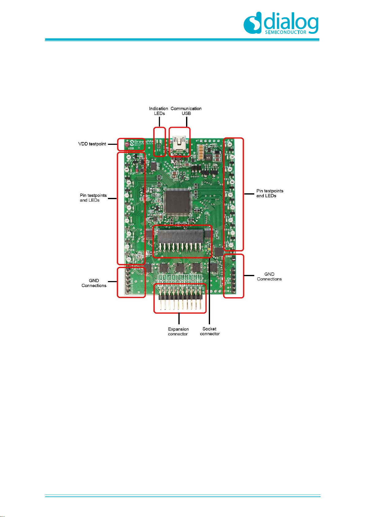
Figure 1: GreenPAK Advanced Development Board, Top View
Note: all test points were designed only for observation of signals on the pins. Please do not
try to connect external power/signal source to test points, this will affect GreenPAK Advanced
Development Board functionality and may even damage it.
4.2 Functional Description
4.2.1 Power Supply
The main power source of the GreenPAK Advanced Development Board is the USB power line. The
Development Board can deliver power from 0 to 5.5 V. To provide this power range, the
Development Board is equipped with a boost converter. A Signal generator with a buffered output
controls the GreenPAK chip power rail. For more information about GreenPAK electrical
specification, please refer to the datasheet.
UM-GP-002
GreenPAK Advanced Development Platform
User Manual
Revision 2.2
21-Feb-2020
CFR0012
8 of 40
© 2020 Dialog Semiconductor
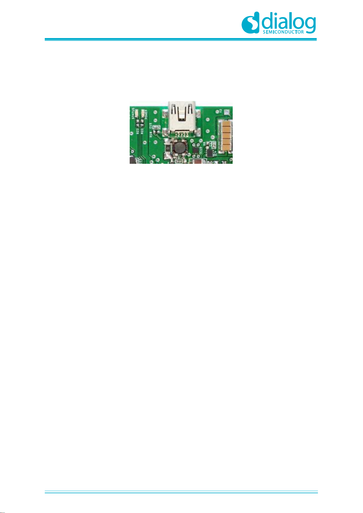
4.2.2 USB Communication
The board has the USB communications interface that uses the USB mini-B connector, as shown in
Figure 2. This interface provides communication with the software control tool and supplies power to
the platform, as discussed in 4.2.1.
Figure 2: USB Interface
4.2.3 GND Connections
There are 6 GND pins on the left side, 6 pins and 1 header on the right side. These can be used for
test equipment (oscilloscope, multimeter, and others) ground reference connection or to connect
external test circuitry ground.
4.2.4 Pin Test Points
Each GreenPAK chip pin including VDD has its own observation test point. These test points were
designed only for observation. To connect an external signal source use a software-controlled
expansion connector.
4.2.5 LEDs
All the pins except Pin 2 can be connected to buffered LEDs. This option allows visualization of
digital levels on chip pins. There are 2 selection modes:
▪Buffered LED (with high impedance input)
▪Inverted Buffered LED (with high impedance input)
This option can be enabled in GreenPAK Designer.
4.2.6 Socket Connector
The GreenPAK Advanced Development Board should be used with a detachable socket board. Its
main purpose is to connect the GreenPAK chip to the Development Board. It‘s easy to use the
programmed chip in external circuits, or to measure current consumption of the project.
4.2.7 Expansion Connector
This port was designed to connect the GreenPAK Advanced Development Board to external circuits
and apply external power, signal sources and loads. It can be used to apply the GreenPAK chip into
your custom design with minimal additional tools. For schematic diagram refer to Figure 3.

UM-GP-002
GreenPAK Advanced Development Platform
User Manual
Revision 2.2
21-Feb-2020
CFR0012
9 of 40
© 2020 Dialog Semiconductor
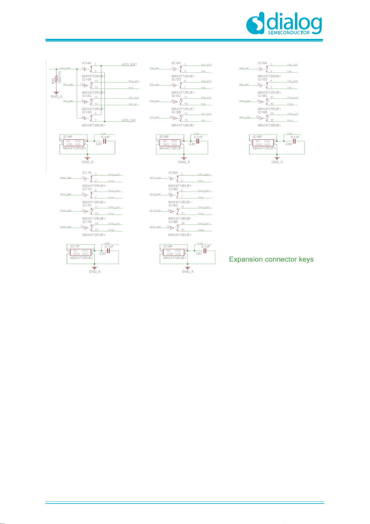
Figure 3: GreenPAK Expansion Connector Schematic
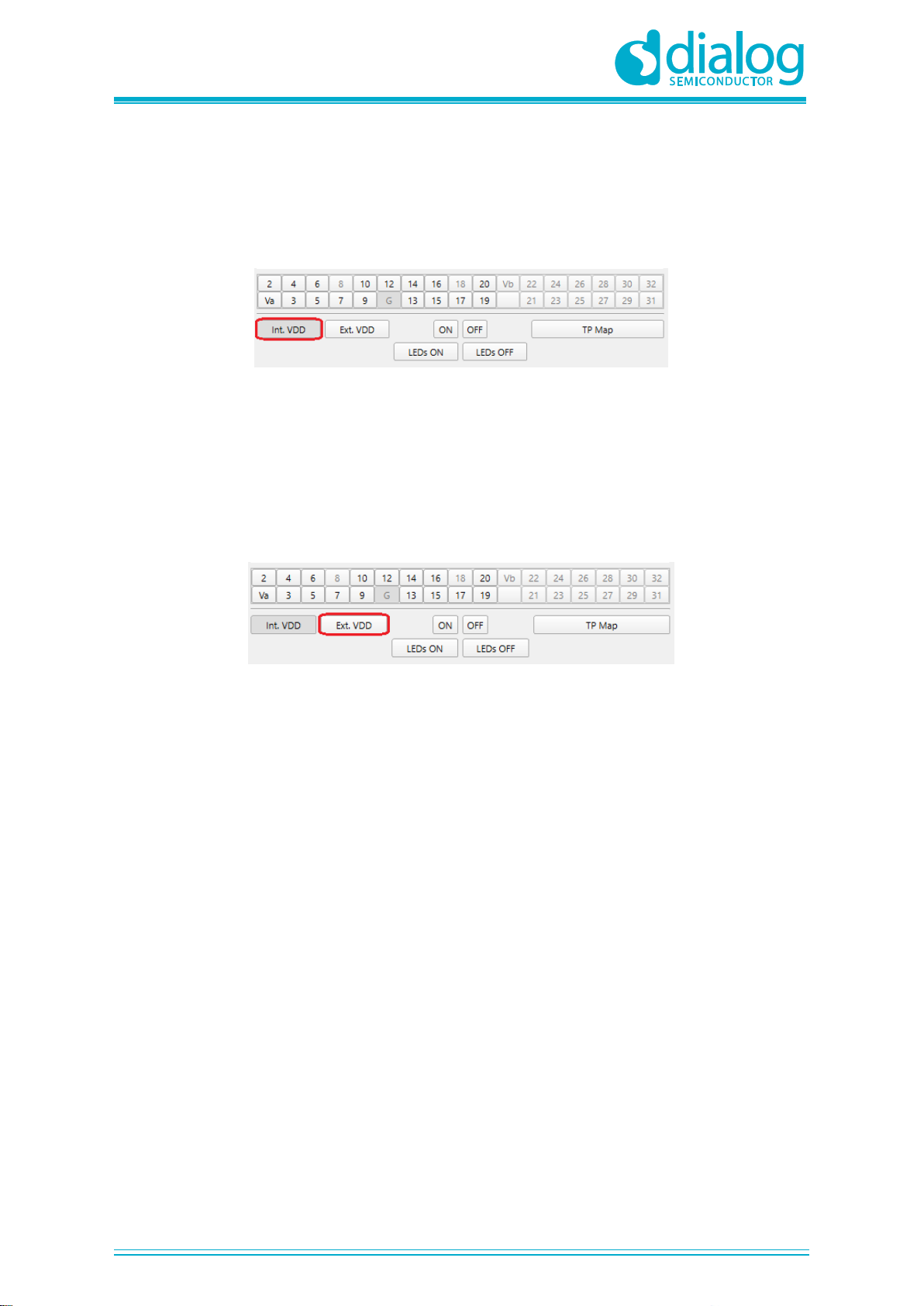
Each pin except Pin 11 (GND) is controlled through an individual analog switch. Expansion connector
is a standard 0.1” double row connector. GreenPAK Designer can enable or disable external pins, as
it is shown in the Figure 4. The main purpose of the Expansion connector is to connect an external
signal/power source safely to the GreenPAK Advanced Development Board.
Figure 4: Expansion Connector Control in GreenPAK Designer
Figure 5 demonstrates the schematic diagram of the expansion connector control.
UM-GP-002
GreenPAK Advanced Development Platform
User Manual
Revision 2.2
21-Feb-2020
CFR0012
10 of 40
© 2020 Dialog Semiconductor
Figure 5: Socket and Expansion Connector Schematic
Expansion connector is enabled only in Emulation mode or Test mode. To enter either of these two
modes the GreenPAK chip must be in the socket. When the Test mode button is pressed the
software will first read the chip to verify if it was inserted and then configure the GreenPAK Advanced
Development Board as set in Emulation Tool window. When the Test mode button is gray then the
Development Platform is in Default state and all expansion port switches are open (disconnected).
After Emulation button is pressed, the software will automatically perform the following steps:
▪check chip presence
▪open all expansion port switches (external signals/loads can be left connected to expansion port)
▪use internal power and load configuration to the chip
▪only for case #3: adjust internal power source to external power level → close external power
switch → open internal power switch
▪configure Development Board as set in Emulation Tool window
Parasitic effects should be also considered while using the GreenPAK Advanced Development Board
in-circuit with analog signals. The entire Development Board circuitry along with the wiring have a
significant amount of mutual capacitance and inductance. The detachable socket can also be used
for the in-circuit development with programmed chips (the Development Board and socket
connectors have the same pinout).
The GreenPAK Advanced Development Board provides three possible ways of using expansion
connector:
1) Internal power is used to run the chip, no external power output is needed, external signal
sources and loads can be connected between pins and GND.
UM-GP-002
GreenPAK Advanced Development Platform
User Manual
Revision 2.2
21-Feb-2020
CFR0012
11 of 40
© 2020 Dialog Semiconductor
The configuration steps:
▪close internal and open external power switch
▪close all used expansion port switches in the software
▪hit Emulation/Test mode button
This is the common way of using an Expansion connector.
Figure 6: Internal Power Source
2) Internal power is used to run the chip and external circuit (internal power source/sink current is
limited to 50 mA).
The configuration steps:
▪close internal power switch
▪close external power switch
▪close all used expansion port switches in the software
▪hit Emulation/Test mode button
Figure 7: Internal Power Source for GreenPAK Chip and External Development Platform
3) External power is used to run the chip and external circuit (internal source output is in Hi-Z state).
The configuration steps:
▪open internal power switch
▪close external power switch
▪close all used expansion port switches in the software
▪hit Emulation/Test mode button (External power should be applied before this step)
Note that the GreenPAK chip has internal OTP memory which is normally loaded into RAM registers
at initialization time.“Emulation mode” will bypass this load, and write the updated version of the
project directly into the RAM register inside the GreenPAK chip many times, but after power loss all
internal data will be lost. When the GreenPAK chip is already programmed the user can use
Emulation mode to load another project and test it on the emulation tool in Emulation mode, in that
case emulation data will be cleared. The “Emulation” mode is not necessary for checking
programmed parts: in this case the “Test mode” is used.
Expansion connector can be divided by types of connections:
1. VDD
2. GND
3. Data connections
The VDD connection enables the user to connect/disconnect external and internal power source. This
connection meets next requirements:
▪External power range: 1.8 - 5.5 V
▪High resistance voltage dividers are not recommended
UM-GP-002
GreenPAK Advanced Development Platform
User Manual
Revision 2.2
21-Feb-2020
CFR0012
12 of 40
© 2020 Dialog Semiconductor
The GND connection is connected directly to the Development Board, and cannot be controlled by
GreenPAK Designer.
Data connections are the easiest way to connect external lines to the GreenPAK chip. They are
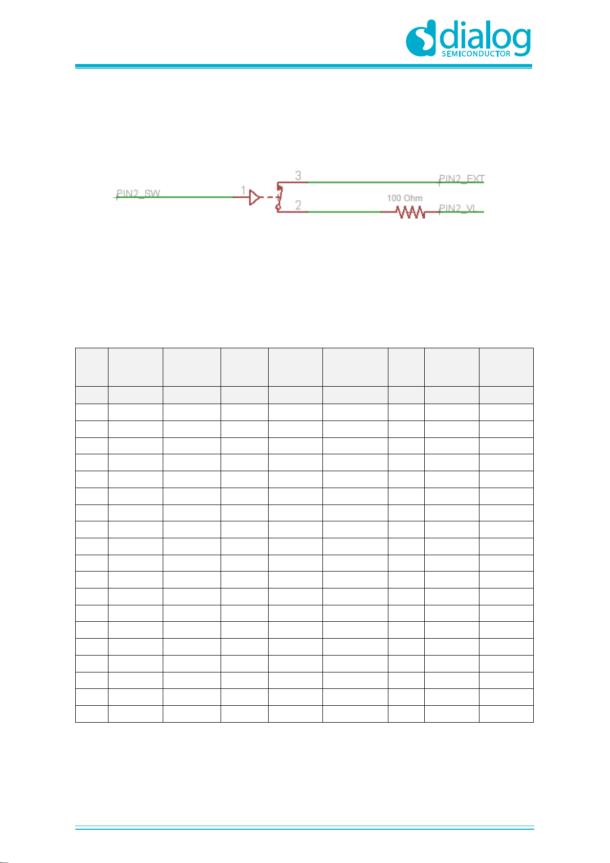
software controlled switches. Every line is connected with a 100 W resistor.
Figure 8: Expansion Connector. Pin with Protection Resistor
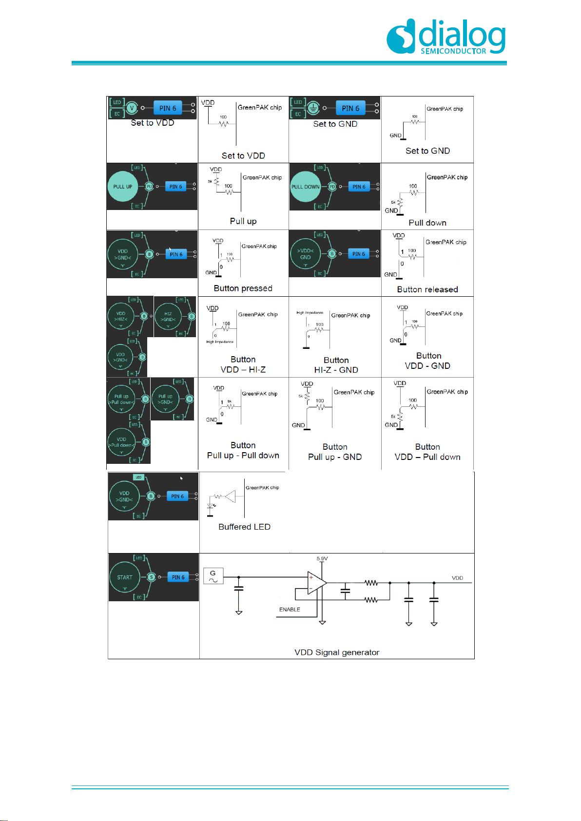
4.2.8 Pins Connectivity
The GreenPAK Advanced Development Board supports connecting eight types of loads and signal
sources. Each source has its own special purpose. The List of available connections for each test
point is presented in Table 1.
Table 1: Available Connections for Each Test Point
Pin
Set to VDD
Set to GND
Pull-up
Pull-down
Set
Configurable
Button
LED
Signal
Generator
Logic
Generator
#
1
2
3
4
5
6
7
8
VDD
-
-
-
-
-
-
+
-
TP2
+
+
+
+
+
-
-
+
TP3
+
+
+
+
+
+
-
+
TP4
+
+
+
+
+
+
-
+
TP5
+
+
+
+
+
+
-
+
TP6
+
+
+
+
+
+
+
+
TP7
+
+
+
+
+
+
+
+
TP8
+
+
+
+
+
+
+
+
TP9
+
+
+
+
+
+
-
+
TP10
+
+
+
+
+
+
+
+
TP12
+
+
+
+
+
+
+
+
TP13
+
+
+
+
+
+
+
+
TP14
+
+
+
+
+
+
+
+
TP15
+
+
+
+
+
+
-
+
TP16
+
+
+
+
+
+
-
+
TP17
+
+
+
+
+
+
-
+
TP18
+
+
+
+
+
+
-
+
TP19
+
+
+
+
+
+
-
+
TP20
+
+
+
+
+
+
-
+
UM-GP-002
GreenPAK Advanced Development Platform
User Manual
Revision 2.2
21-Feb-2020
CFR0012
13 of 40
© 2020 Dialog Semiconductor
Figure 9: Pin Signal Sources/Loading Schematics
Note: VDD Signal generator works similar to other Signal generators but has wider output
voltage range. It can provide maximum supply level of 5.5 V.
Set to Pull up
Button pressed
Button released
Button with
different
configurations
Set to Pull down
VDD Signal
generator
LED
UM-GP-002
GreenPAK Advanced Development Platform
User Manual
Revision 2.2
21-Feb-2020
CFR0012
14 of 40
© 2020 Dialog Semiconductor
5 Example Projects using SLG46721
5.1 Project: Counter with Clock Enable
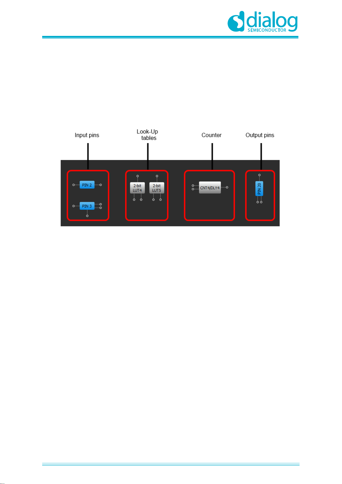
Blocks required:
▪2 digital inputs
▪1 digital output
▪1 Look Up Table with two inputs
▪1 Counter
Figure 10: GreenPAK Designer
UM-GP-002
GreenPAK Advanced Development Platform
User Manual
Revision 2.2
21-Feb-2020
CFR0012
15 of 40
© 2020 Dialog Semiconductor
Figure 11: GreenPAK Components List
UM-GP-002
GreenPAK Advanced Development Platform
User Manual
Revision 2.2
21-Feb-2020
CFR0012
16 of 40
© 2020 Dialog Semiconductor
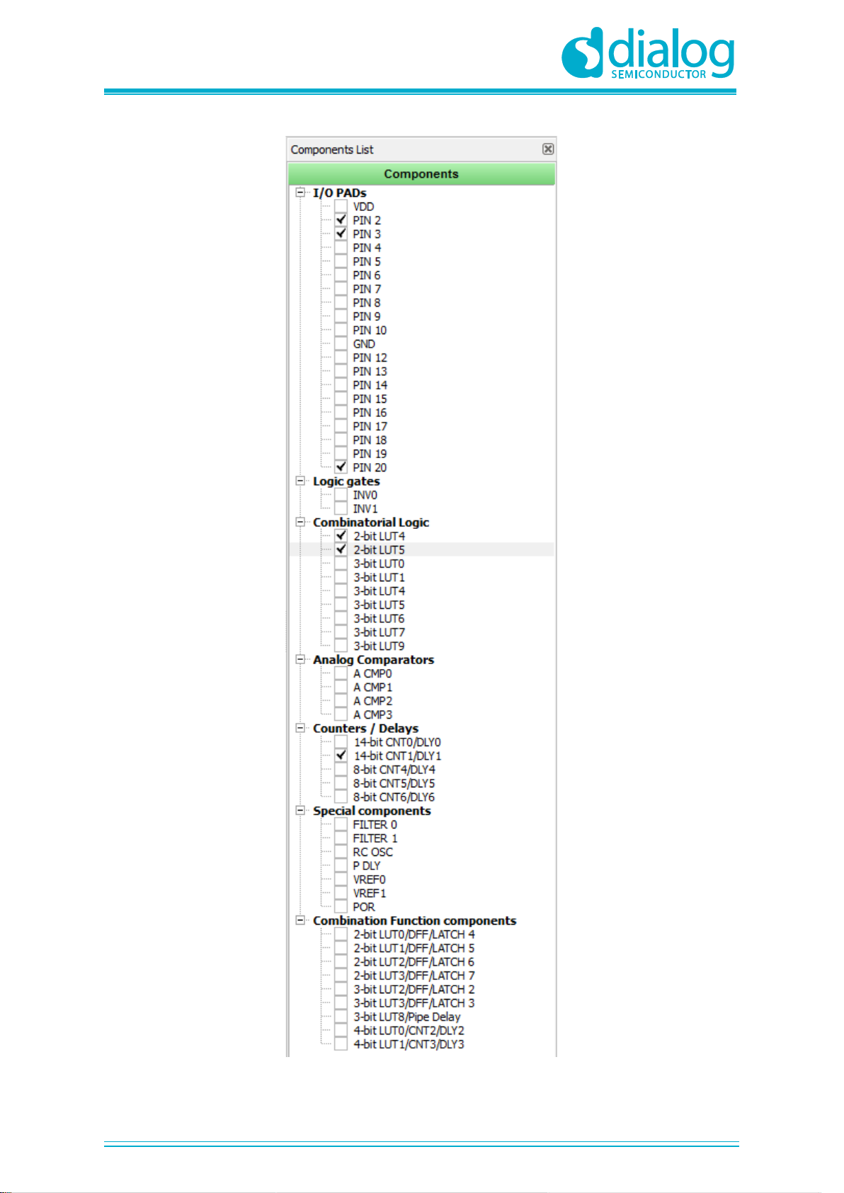
All these components can be found in components list. If there are no components on the work area -
make sure this component is enabled.
Table 2: Pin Configuration for Counter with Clock Enable
Pin #
Pin Name
Type
Pin Description
1
VDD
PWR
Supply Voltage
2
Clock
Digital input
Digital input
3
Enable
Digital Input
Digital Input
11
GND
GND
Ground
20
Counter Output
Push-Pull output
Digital input
All components used in the project are shown in Figure 10, next step is to configure selected blocks.
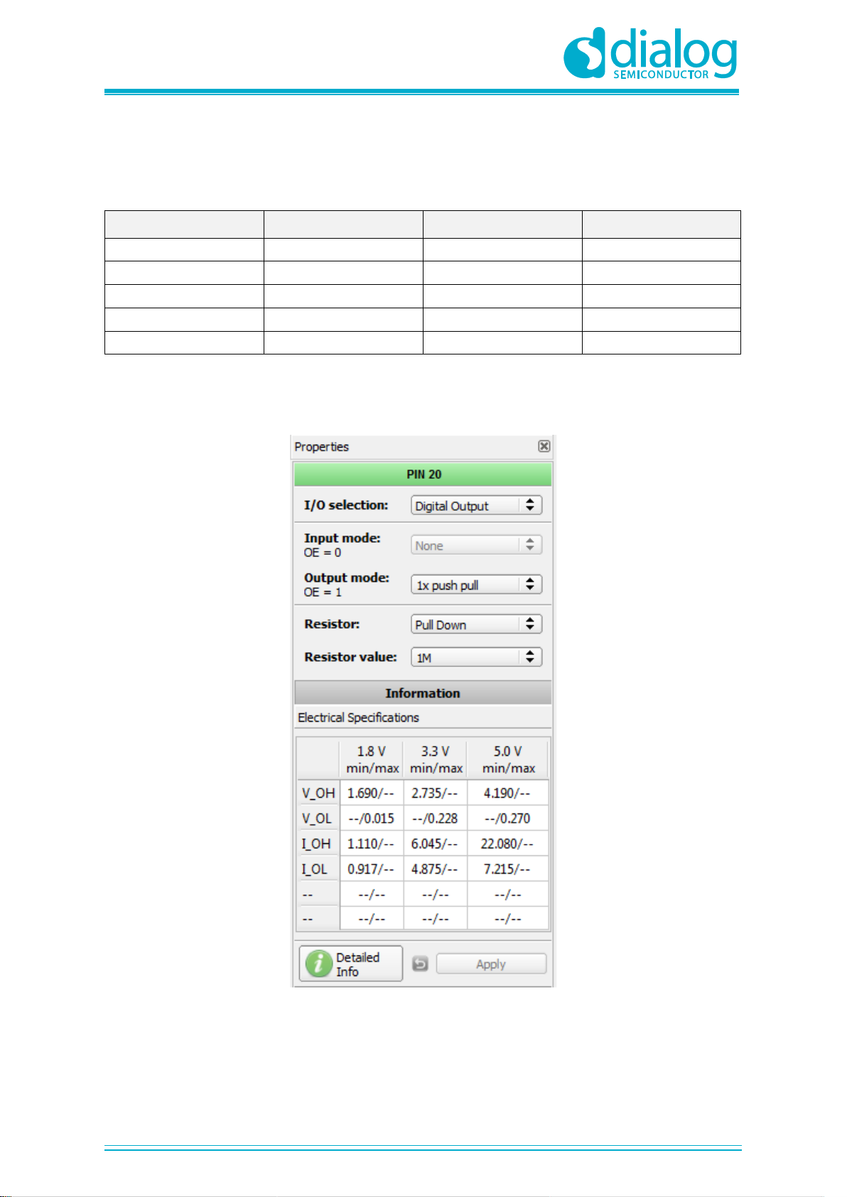
Double click on Pin 20 to open “Properties” panel. Select “1x push pull” from the drop-down menu in
Pin 20 properties and hit “Apply” button.
Figure 12: Pin 20 Mode
UM-GP-002
GreenPAK Advanced Development Platform
User Manual
Revision 2.2
21-Feb-2020
CFR0012
17 of 40
© 2020 Dialog Semiconductor
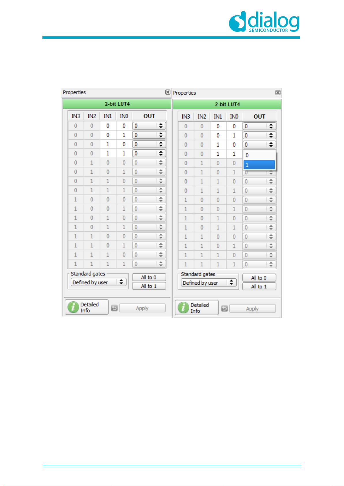
The next component in this design is the Look Up Table. First Look Up Table (LUT4) is used to
generate logic “1” only when there are high logic levels on both inputs (AND gate). Select AND gate
from “Standard gates” drop-down menu or set table manually. Second Look Up Table (LUT5) is
configured as NOR gate. It is used to generate reset signal for counter on Pin 3 falling edge.
Figure 13: Look Up Table Properties Configured as AND Gate

UM-GP-002
GreenPAK Advanced Development Platform
User Manual
Revision 2.2
21-Feb-2020
CFR0012
18 of 40
© 2020 Dialog Semiconductor
Figure 14: Look Up Table Properties Configured as NOR Gate
UM-GP-002
GreenPAK Advanced Development Platform
User Manual
Revision 2.2
21-Feb-2020
CFR0012
19 of 40
© 2020 Dialog Semiconductor
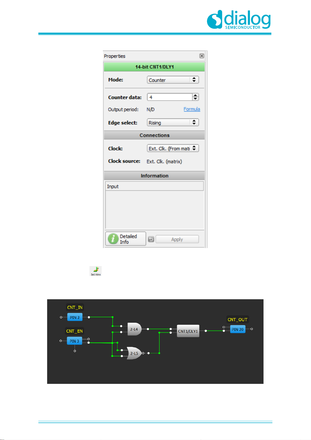
Figure 15: Counter Properties
The final step is to connect used components. Use Wire tool to perform this action. To connect two
pins select “Set Wire” and then click on the first and the second pin of the module or modules
that you want to connect. The trace will be automatically routed.
Figure 16: GreenPAK Designer
Figure 16 displays ready project with configured blocks and wire connections.
UM-GP-002
GreenPAK Advanced Development Platform
User Manual
Revision 2.2
21-Feb-2020
CFR0012
20 of 40
© 2020 Dialog Semiconductor
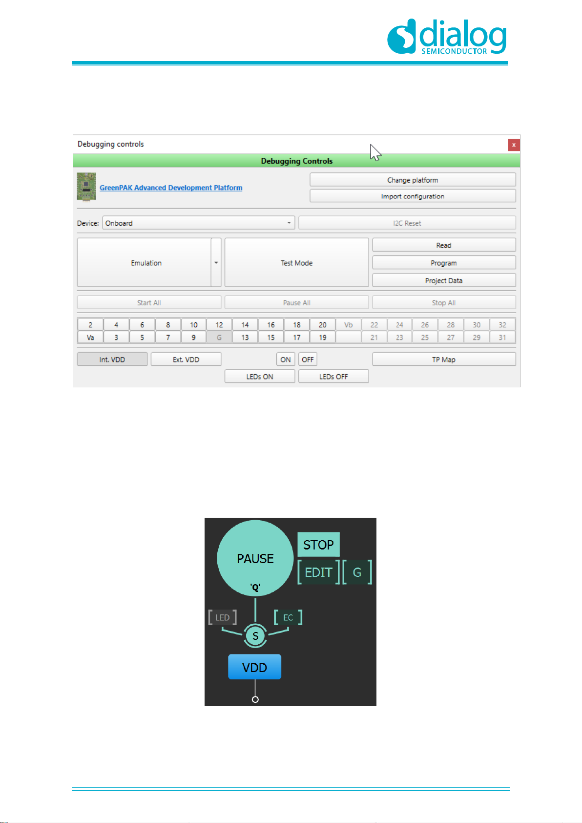
Use the GreenPAK Advanced Development Board to test this project. Connect the GreenPAK
Advanced Development Board to the PC and press “Emulation” button. This will load the code of
your project to the chip and will enable Test functionality of your Development Board.
Figure 17: GreenPAK Designer, Emulation Tool
To test this project we will use the following tools:
▪Signal generator. Signal generator is applied to VDD pin to power GreenPAK chip
▪Logic generator. Logic generator serves as clock source
▪Button is a software simulation of the real button. It switches Pin between VDD and GND signal
levels
▪Inverted buffered LED
▪Buffered LED
Figure 18: Signal Generator Connected to VDD Pin
Signal generator is presented as a power source for GreenPAK chip. It's configured to output source
constant 3.3 V.
Table of contents
Other Dialog Semiconductor Motherboard manuals

Dialog Semiconductor
Dialog Semiconductor DA1468 series User manual

Dialog Semiconductor
Dialog Semiconductor DA852 Series User manual

Dialog Semiconductor
Dialog Semiconductor DA7212 User manual

Dialog Semiconductor
Dialog Semiconductor DA16600 User manual

Dialog Semiconductor
Dialog Semiconductor SLG46824 Operating instructions

Dialog Semiconductor
Dialog Semiconductor DA9155M User manual

Dialog Semiconductor
Dialog Semiconductor DA1468 series Installation and operating instructions

Dialog Semiconductor
Dialog Semiconductor UM-GP-007 User manual


