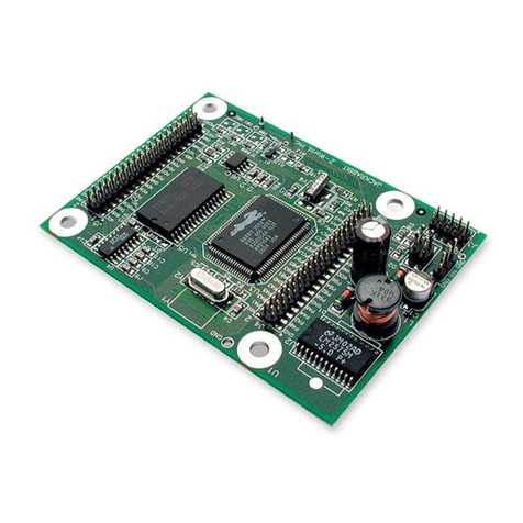
Digi NS9750 User manual

NS9750 Jumpers and Components
90000529_C


Part number/version: 90000529_C
Release date: March 2006
www.digi.com
NS9750 Jumpers and
Components

Digi International
11001 Bren Road East
Minnetonka, MN 55343 U.S.A.
United States: +1 877 912-3444
Other locations: +1 952 912-3444
www.digi.com/support/
www.digi.com
©2005-2006 Digi International Inc.
Printed in the United States of America. All rights reserved.
Digi, Digi International, the Digi logo, the Making Device Networking Easy logo, NetSilicon, a Digi
International Company, NET+, NET+OS and NET+Works are trademarks or registered trademarks of Digi
International, Inc. in the United States and other countries worldwide. All other trademarks are the
property of their respective owners.
Information in this document is subject to change without notice and does not represent a committment
on the part of Digi International.
Digi provides this document “as is,” without warranty of any kind, either expressed or implied, including,
but not limited to, the implied warranties of, fitness or merchantability for a particular purpose. Digi may
make improvements and/or changes in this manual or in the product(s) and/or the program(s) described
in this manual at any time.
This product could include technical inaccuracies or typographical errors. Changes are made periodically
to the information herein; these changes may be incorporated in new editions of the publication.
Contents
iii
Overview .................................................................................. 2
NS9750 development board features .......................................... 2
GPIO-related configurations ........................................................... 3
Default configurations ........................................................... 3
IEEE 1284 parallel port configuration alternatives .......................... 4
USB host ............................................................................ 4
USB device ......................................................................... 4
Serial port B in RS232, full modem control ................................... 4
Serial port D in RS232, full modem control................................... 5
Non GPIO-related configurations ...................................................... 5
Serial port A 422/485 mode ..................................................... 5
PCI CardBus ........................................................................ 5
Mini-PCI............................................................................. 5
RMII ................................................................................. 6
PCI or CardBus..................................................................... 6
Default configuration switch settings ................................................ 7
Configuration register switch settings................................................ 9


v
Using This Guide
Review this section for basic information about this guide, as well as for general
support contact information.
About this guide
This guide provides information about the jumpers, components, and configuration of
the NS9750 development board. The NS9750, part of the Digi NET+ARM line of SoC
(System-on-Chip) products, supports any type of high bandwidth application in
Intelligent Networked Devices.
The NET+ARM is part of the NET+Works integrated product family, which includes the
NET+OS network software suite.

vi
NS9750 Jumpers and Components, Rev. C 03/2006
Who should read this guide
This guide is for hardware developers, system software developers, and application
programmers who want to use the NS9750 for development.
To complete the tasks described in this guide, you must:
Understand the basics of hardware and software design, operating systems,
and microprocessor design.
Understand the NS9750 architecture.
What’s in this guide
The NS9750 Jumpers and Components describes the use and configuration of the
NS9750 development board.
Conventions used in this guide
This table describes the typographic conventions that may be used in this guide:
This convention Is used for
italic type Emphasis, new terms, variables, and document titles.
bold, sans serif type Menu commands, dialog box components, and other items
that appear on-screen.
Select Menu →option Menu commands. The first word is the menu name; the
words that follow are menu selections.
monospaced type Filenames, pathnames, and code examples.

www.digi.com
vii
Using This Guide
Related documentation
For information on the chip you are using, see the NS9750 Hardware
Reference.
For NS9750 schematics and BOM, review the documentation CD-ROM that
came with your development kit.
See the NET+OS software documentation for information appropriate to the
chip you are using.
Documentation updates
Digi occasionally provides documentation updates on the Web site.
Be aware that if you see differences between the documentation you received in your
NET+Works package and the documentation on the Web site, the Web site content is
the latest version.
Customer support
To get help with a question or technical problem with this product, or to make
comments and recommendations about our products or documentation, use the
contact information listed in this tables.
For Contact information
Technical support Telephone: 1 877 912-3444/ 1 952 912-3456
Fax: 1 952 912-4960
Documentation [email protected]
Digi home page www.digi.com
Online problem reporting www.digi.com/support/eservice/eservicelogin.jsp


1
NS9750 Jumpers and
Components
The NS9750 Jumpers and Components provides a description of the NS9750
development board. This document also explains the board’s default states and
provides information for configuring other states.

Overview
2
NS9750 Jumpers and Components, Rev. C 03/2006
Overview
The NS9750 contains 50 GPIO pins. Each of the 50 pins can be multiplexed to provide
up to four different functions. The NS9750 development board implements each of
the optional functions. See the NS9750 Hardware Reference for more information
about the options for each pin.
The development board uses 0 ohm resistors to enable the functions.
You can identify the board by the following information:
Market name. NS9750 development board
NS9750. A 32-bit, 200MHz NET+ARM processor
NS9750 development board features
The NS9750 development board provides these basic features:
200MHz NS9750
16 MB 100MHZ SDRAM, 8 MB flash, 1 MB serial EEPROM (serial EEPROM
connected to SPI port B)
10/100 Mbps MII PHY, magnetics and RJ45 connector
10/100 Mbps RMII PHY, magnetics and RJ45 connector
10/100 Mbps MII connector
CardBus socket and mini-PCI v1.0
32-bit PCI v2.2 supported (connector included)
USB OHCI host and device connectors, with PnP support for USBd
Up to quad RS232 or 485, SPI, and two HDLC serial I/O supported
–Default to 1xSPI, 1x8-pin RS232, and 1x4-pin RS232
I2C connector plus 4-pin header
Generic header for 8-bit LCD (up to 24-bit can be supported)
1284 peripheral supported (connector included)
SO-DIMM connector for external peripherals
Tw o t i m e r s

www.digi.com
3
NS9750 Jumpers and Components
Three diagnostic LEDs (five supported)
20-pin JTAG header
Reset pushbutton switch
Full schematics and BOM available (see your hardware CD and the Digi Web
site)
Supported interfaces, in some cases, must be customer-enabled (using
jumper, switch, or resistor changes)
GPIO-related configurations
Table 1 shows the default configuration for the NS9750 development board. The
remainder of this section provides options for configuring the development board in
other, common ways. See also the GPIO resistor matrix, available on your hardware
CD, to determine additional configurations.
Default configurations
Default function Description
SPI on port B Can boot from SEEPROM or connect to a 4-pin header.
Serial port on port A Full modem control, RS232 mode.
8-bit LCD LCD available using headers P34 and P36.
Serial port on port C TX, RX, RTS, and CTS available in RS232 mode.
LEDs 1-5 Available on GPIO16, GPIO17, GPIO45, GPIO46, and
GPIO47. The LEDs are not available when R140–R144 are
removed. The default configuration has CR5 and CR6
unavailable.
GPIO44 Available on P21 pin 5.
GPIO39 Available on P23 pin 8.
USB host USB host available on P31 USB “A-type” connector.
Table 1: NS9750 development board default configuration

GPIO-related configurations
4
NS9750 Jumpers and Components, Rev. C 03/2006
IEEE 1284 parallel port configuration alternatives
Populate these resistors with 0 ohm jumpers: RN34, RN35, R538, R544.
Unpopulate these resistors: RN42, R8, R9, R136, R140–R142, R144, R335–
R338, R355–R357, R406.
Be sure these resistors are unpopulated: RN44, RN45, RN36, RN37, RN38,
RN39, R150, R162, R163, R165, R169, R171, R172, R173, R178, R180, R187,
R195, R197, R373–R376, R386–R393, R407–R409, R422, R427–R429, R434,
R438, R441, R449, R464, R474–R476, R478, R482, R502, R510, R514, R518,
R519, R534, R535, R539, R540.
USB host
Populate these resistors with 0 ohm jumpers: R137 and R136 (default).
Unpopulate these resistors: R143 and R144 (default).
Be sure these resistors are unpopulated: R187, R394, R395, R519, R544
(default).
Set SW9 switches 1 and 3 to ON (default).
USB device
Populate this resistor with 0 ohm jumper: R139.
Unpopulate this resistor: R137.
Be sure these resistors are unpopulated: R395, R143.
Set SW9 switch 2 to ON for device.
Set SW9 switch 4 to ON for low-speed device.
Serial port B in RS232, full modem control
Populate these resistors with 0 ohm jumpers: R150, R151, R180, R191, R422,
R449, R450, R486.
Unpopulate this resistor: RN42.
Be sure these resistors are unpopulated: RN35, RN44, R185, R190, R370–
R377, R423–R429, R488, R496, R509.

www.digi.com
5
NS9750 Jumpers and Components
Serial port D in RS232, full modem control
Populate these resistors with 0 ohm jumpers: R154, R155, R164, R464, R474,
R483, R502, R518.
Unpopulate these resistors: RN33, R140–R142, R159, R160, R406.
Be sure these resistors are unpopulated: RN35, RN36, RN39, R186,
R407–R409, R430–R433, R490, R507.
Non GPIO-related configurations
The non GPIO-related configurations are based on this setup: looking directly into the
DB9 connectors and going clockwise, the upper right port is port B, the lower right
port is port A, the lower left port is port C, and the upper left port is port D.
Serial port A 422/485 mode
XTo change full modem RS232 serial port A into RS422/485 mode:
1Change SW18 switch 1 to OFF.
2Change SW18 switch 3 to ON; this changes RS422/485 to 2-wire mode.
3Change SW18 switch 4 to ON, to use on board termination.
PCI CardBus
To ensure that PCI CardBus is the default, be sure that SW10 switch 5 is turned ON.
Mini-PCI
To use mini-PCI, be sure that SW10 switch 5 is turned OFF.

Non GPIO-related configurations
6
NS9750 Jumpers and Components, Rev. C 03/2006
RMII
XTo use RMII on Ethernet jack labeled P14:
Populate these resistors with 0 ohm resistors: R75, R77, R84, R91, R97,
R118, R300, R302, R316, R317, R328, R331, R332, R603, and RN74.
Unpopulate these resistors: R106, R117, R127, R129, R342, R600, R604,
RN21, RN25.
RN74 pin 9 trace needs to be cut. An alternate method is to shift RN74 over
so the pin 8-to-pin 9 connection is not made.
PCI or CardBus
Be sure that your board corresponds to the interface type you purchased: PCI or
CardBus. Contact your Application Engineer for information.

www.digi.com
7
NS9750 Jumpers and Components
Default configuration switch settings
Table 2 shows the default configuration settings for the NS9750 development board
and explains each setting.
Switch Switch setting Description
SW1 Switch 1 = ON
Switch 2 = OFF
Switch 3 = OFF
Switch 4 = OFF
Selects static chip select 0 for ~CS1 on SRAM
SW2 Switch 1 = OFF
Switch 2 = OFF
Switch 3 = OFF
Switch 4 = ON
Selects static chip select 3 for ~CS4 on SRAM
SW3 Switch 1 = OFF
Switch 2 = OFF
Switch 3 = ON
Switch 4 = OFF
Selects static chip select 2 for ~CS2 on SRAM
SW4 Switch 1 = OFF
Switch 2 = OFF
Switch 3 = ON
Switch 4 = OFF
Switch 5 = OFF
Switch 6 = ON
Switch 7 = OFF
Switch 8 = OFF
Selects address(13) for bank address(0) on SDRAM
and address(14) for bank address(1) on SDRAM
SW8 Switch 1 = OFF
Switch 2 = OFF
Switch 3 = ON
Switch 4 = OFF
Selects NS9750 as a host for PCI
Table 2: Default configuration switch settings

Default configuration switch settings
8
NS9750 Jumpers and Components, Rev. C 03/2006
SW9 Switch 1 = ON
Switch 2 = OFF
Switch 3 = ON
Switch 4 = OFF
Selects NS9750 as USB host
Switch 1 = OFF
Switch 2 = ON
Switch 3 = OFF
Switch 4 = OFF
Selects NS9750 as USB device
Switch 1 = OFF
Switch 2 = OFF
Switch 3 = OFF
Switch 4 = ON
Implements slow speed USB device
Switch Switch setting Description
Table 2: Default configuration switch settings

www.digi.com
9
NS9750 Jumpers and Components
Configuration register switch settings
Table 3 provides switch settings and descriptions for several configuration registers.
See the NS9750 Hardware Reference for more information about the configuration
registers.
Note:
For SW17 – SW20, switches 3 and 4 are RS485/422 options for their
respective ports.
Switch Switch setting Description
SW10 Switch 1 = OFF
Switch 2 = OFF
Switch 3 = OFF
Switch 4 = ON
Switch 5 = ON
Switch 6 = ON
Switch 7 = OFF
Switch 8 = ON
rtck
boot_strap[4]
boot_strap[3]
boot_strap[2]
boot_strap[1]
boot_strap[0]
GPIO[49]
GPIO[44]
SW11 Switch 1 = OFF
Switch 2 = OFF
Switch 3 = OFF
Switch 4 = ON
Switch 5 = OFF
Switch 6 = OFF
Switch 7 = OFF
Switch 8 = OFF
reset_done
GPIO[24]
GPIO[20]
GPIO[19]
GPIO[17]
GPIO[12]
GPIO[10]
GPIO[8]
SW12 Switch 1 = OFF
Switch 2 = OFF
Switch 3 = OFF
Switch 4 = OFF
Switch 5 = OFF
Switch 6 = OFF
Switch 7 = OFF
Switch 8 = OFF
GPIO[4]
GPIO[2]
GPIO[0]
GPIO[41]
GPIO[40]
GPIO[39]
GPIO[38]
GPIO[37]
Table 3: Configuration register switch settings

Configuration register switch settings
10
NS9750 Jumpers and Components, Rev. C 03/2006
SW13 Switch 1 = OFF
Switch 2 = OFF
Switch 3 = OFF
Switch 4 = OFF
Switch 5 = OFF
Switch 6 = OFF
Switch 7 = OFF
Switch 8 = OFF
GPIO[36]
GPIO[35]
GPIO[34]
GPIO[33]
GPIO[32]
GPIO[31]
GPIO[30]
GPIO[29]
SW14 Switch 1 = OFF
Switch 2 = OFF
Switch 3 = OFF
Switch 4 = OFF
Switch 5 = OFF
Switch 6 = OFF
Switch 7 = OFF
Switch 8 = OFF
GPIO[28]
GPIO[27]
GPIO[26]
GPIO[25]
GPIO[23]
GPIO[22]
GPIO[21]
GPIO[18]
SW15 Switch 1 = OFF
Switch 2 = OFF
Switch 3 = OFF
Switch 4 = OFF
Switch 5 = OFF
Switch 6 = OFF
Switch 7 = OFF
Switch 8 = OFF
GPIO[16]
GPIO[15]
GPIO[14]
GPIO[13]
GPIO[11]
GPIO[9]
GPIO[7]
GPIO[6]
SW16 Switch 1 = OFF
Switch 2 = OFF
Switch 3 = OFF
Switch 4 = OFF
Switch 5 = OFF
Switch 6 = ON
Switch 7 = ON
Switch 8 = ON
GPIO[5]
GPIO[3]
GPIO[1]
pll_test_n = low
bist_en_n = low
scan_en_n = low
pll_test_n = high
bist_en_n = high
Switch Switch setting Description
Table 3: Configuration register switch settings
Other manuals for NS9750
1
Table of contents
Other Digi Motherboard manuals

Digi
Digi ConnectCore 8M Nano Quick user guide

Digi
Digi ConnectCore MP15 Quick user guide

Digi
Digi ConnectCore 6 SBC Quick user guide

Digi
Digi ConnectCore MP13 Quick user guide

Digi
Digi NET+50 User manual

Digi
Digi ConnectCore 6UL SBC Pro Quick user guide

Digi
Digi XBee Grove Development Board Series User manual

Digi
Digi BL4S100 User manual

Digi
Digi XBee Grove User manual

Digi
Digi JACKRABBIT BL1800 User manual