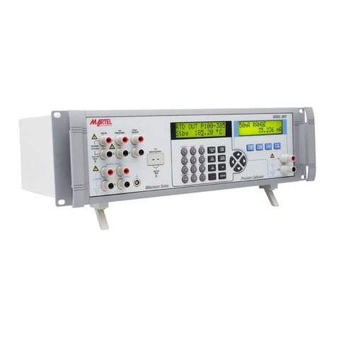
doble f2250 series User manual

F2250 Family of
Power System Simulators
User Guide
Doble Engineering Company
85 Walnut Street
Watertown, Massachusetts 02472-4037
(USA)
PN 500-0096 72A-1146 Rev. D 8/99

TRANS2™, ProTesT™, SSIMUL™, AutoSensE™ and Active Sources™ are registered trademarks of
Doble Engineering.
This Manual is the sole property of the Doble Engineering Company (Doble) and is provided for the
exclusive use of Doble Clients under contractual agreement for Doble Test equipment and
services.
In no event does the Doble Engineering Company assume the liability for any technical or editorial
errors of commission, or omission; nor is Doble liable for direct, indirect, incidental, or
consequential damages arising out of the use or inability to use this Manual.
Government Restricted Rights Legend: Use, Duplication, or disclosure by the U.S. Government is
subject to restrictions as set forth in subparagraphs (c)(1) and (c)(2) of the Commercial Computer
Software - Restricted Rights Clause at FAR 52.227-19.
This manual is protected by copyright, all rights reserved, and no part hereof may be photocopied
or reproduced in any form without prior written consent of the Doble Engineering Company.
Copyright
©
1999
By Doble Engineering Company
All Rights Reserved.

Warranty
Equipment Limited
Warranty
Doble Engineering Company (DOBLE) warrants the products that it
manufactures to be free from defects in material and workmanship for a
period of one year from the date shipped from the factory.
During the one-year warranty period, DOBLE will repair or replace, at its
option, any defective products or components thereof at no additional
charge, provided that the product or component is returned, shipping
prepaid, to DOBLE. The Purchaser is responsible for insuring any product
or component so returned and assumes the risk of loss during shipment.
All replaced products and components become the property of DOBLE.
THIS LIMITED WARRANTY DOES NOT EXTEND TO ANY PRODUCTS
WHICH HAVE BEEN DAMAGED AS A RESULT OF ACCIDENT, MISUSE,
ABUSE, OR AS A RESULT OF MODIFICATION BY ANYONE OTHER
THAN DOBLE OR AN AUTHORIZED DOBLE REPRESENTATIVE.
EXCEPT AS EXPRESSLY SET FORTH ABOVE, NO OTHER WARRANTIES,
EXPRESSED OR IMPLIED, ARE MADE WITH RESPECT TO THE
PRODUCT INCLUDING, BUT NOT LIMITED TO, ANY IMPLIED
WARRANTIES OF MERCHANTABILITY AND FITNESS FOR A
PARTICULAR PURPOSE. DOBLE EXPRESSLY DISCLAIMS ALL
WARRANTIES NOT STATED HEREIN. IN THE EVENT THE PRODUCT IS
NOT FREE FROM DEFECTS AS WARRANTED ABOVE, THE
PURCHASER’S SOLE REMEDY SHALL BE REPAIR OR REPLACEMENT AS
PROVIDED ABOVE. UNDER NO CIRCUMSTANCES WILL DOBLE BE
LIABLE TO THE PURCHASER OR ANY USER FOR ANY DAMAGES,
INCLUDING WITHOUT LIMITATION, PERSONAL INJURY OR
PROPERTY DAMAGE CAUSE BY THE PRODUCT, ANY INCIDENTAL
OR CONSEQUENTIAL DAMAGES, EXPENSES, LOST PROFITS, LOST
SAVINGS, OR OTHER DAMAGES ARISING OUT OF THE USE OF OR
INABILITY TO USE THIS PRODUCT.
Software Limited
Warranty
THIS SOFTWARE PRODUCT IS PROVIDED “AS IS”WITHOUT
WARRANTY OF ANY KIND, EITHER EXPRESSED OR IMPLIED,
INCLUDING, BUT NOT LIMITED TO, THE IMPLIED WARRANTIES OF
MERCHANTABILITY AND FITNESS FOR A PARTICULAR PURPOSE. THE
ENTIRE RISK AS TO THE QUALITY AND PERFORMANCE OF THIS
SOFTWARE PRODUCT IS WITH PURCHASER SHOULD THE
PRODUCT PROVE DEFECTIVE. PURCHASER (AND NOT DOBLE OR
AN AUTHORIZED DEALER) ASSUMES THE ENTIRE COST OF ALL
NECESSARY SERVICING, REPAIR, OR CORRECTION.
Some states do not allow the exclusion of implied warranties, so the
above exclusion may not apply. This warranty gives the purchaser
specific legal rights and you may also have other rights which vary from
state to state.
DOBLE warrants the disks on which the software product is furnished to
be free from defects in materials and workmanship under normal use for
a period of one hundred and twenty (120) days from the date of shipment
from DOBLE.
Limitations of
Remedies
DOBLE’s entire liability and Purchaser’s exclusive remedy shall be:
1. The replacement of any disks not meeting DOBLE’s "Limited
Warranty" which are returned to Doble.
2. If DOBLE is unable to deliver replacement disks which are free from
defects in materials and workmanship, Purchaser may terminate this
agreement. By returning the software product and all copies thereof
in any form and affirming compliance with this requirement in
writing, DOBLE will refund the purchase price.
IN NO EVENT WILL DOBLE BE LIABLE TO PURCHASER FOR ANY
DAMAGES, INCLUDING ANY LOST PROFITS, LOST SAVINGS OR
OTHER INCIDENTAL OR CONSEQUENTIAL DAMAGES ARISING OUT
OF THE USE OR INABILITY TO USE SUCH SOFTWARE PRODUCT,
EVEN IF DOBLE OR AN AUTHORIZED DEALER HAS BEEN ADVISED
OF THE POSSIBILITY OF SUCH DAMAGES, OR FOR ANY CLAIM BY
ANY OTHER PARTY.
SOME STATES DO NOT ALLOW THE LIMITATION OR EXCLUSION OF
LIABILITY FOR INCIDENTAL OR CONSEQUENTIAL DAMAGES, SO
THE ABOVE LIMITATION OR EXCLUSION MAY NOT APPLY.
For Equipment Maintenance, contact:
Customer Service Manager (Extension 321)
Doble Engineering Company
85 Walnut Street
Watertown, MA 02472 (USA)
Telephone: 617-926-4900
FAX: 617-926-0528
Email: [email protected]

72A-1146 Rev. D 8/99 i
Contents
Preface ......................................................................................................... xiii
Structure of This Manual .......................................................................................................xiv
Document Conventions..........................................................................................................xv
1. Overview of Features and Options ............................................................1-1
Plug-in Options.................................................................................................................... 1-4
Simulator Automation Options............................................................................................. 1-7
Features................................................................................................................................ 1-8
I/O Interface Panel .............................................................................................................1-13
Networked Systems ............................................................................................................1-14
System Communication................................................................................................1-15
Safety .................................................................................................................................1-16
High Voltage Alarm...................................................................................................... 1-16
Automation and Remote Control........................................................................................1-17
F2010 Minicontroller.................................................................................................... 1-17
Host Computer .............................................................................................................1-18
Automatic Protective Relay Testing - ProTesT ...............................................................1-19
Transient Testing - TRANS2 .......................................................................................... 1-20
DobleCoL..................................................................................................................... 1-21
Upgrades and Differences from the F2153 .........................................................................1-22
2. Operating Controls, Indicators, and Displays ............................................2-1
Powering Up........................................................................................................................ 2-1
System Controls and Indicators............................................................................................. 2-2
Source Controls, Indicators, and Displays............................................................................. 2-7
High Voltage Alarm ........................................................................................................ 2-7
Source 1 and Source 2.................................................................................................... 2-7
Phase Angle.................................................................................................................... 2-8
Amplitude ...................................................................................................................... 2-9
On/Enable ....................................................................................................................2-10
Hertz ............................................................................................................................2-10
Range ...........................................................................................................................2-13

ii 72A-1146 Rev. D 8/99
Timer Controls, Indicators and Displays............................................................................. 2-18
Time............................................................................................................................. 2-18
Reset ............................................................................................................................ 2-19
Start and Stop ............................................................................................................... 2-19
Timer Logic Inputs and Outputs ................................................................................... 2-20
Configuration Messages and Displays ................................................................................ 2-22
Minicontroller F2010 Controls and Indicators.................................................................... 2-23
Controls ....................................................................................................................... 2-23
Battery Simulator Controls and Indicators .......................................................................... 2-28
3. Setup and Operation ................................................................................. 3-1
Set Up.................................................................................................................................. 3-1
Multi-Unit Systems............................................................................................................... 3-2
Controller-in-Charge ...................................................................................................... 3-3
Connection and Power-Up............................................................................................. 3-4
Configuration....................................................................................................................... 3-8
Base Frequency .............................................................................................................. 3-8
Source Designations....................................................................................................... 3-9
Source Parameters........................................................................................................ 3-10
Ramping....................................................................................................................... 3-11
Timer Configuration ..................................................................................................... 3-12
Options.............................................................................................................................. 3-13
Fault Rotate - F2810 Option......................................................................................... 3-13
Battery Simulator - F2875 Option................................................................................. 3-16
Precision Autosynchronizer - F2920 Option................................................................. 3-16
Minicontroller - F2010 ................................................................................................. 3-22
4. Principles of Operation ............................................................................. 4-1
Theory of Operation ..................................................................................................... 4-1
Organization........................................................................................................................ 4-2
Operation ............................................................................................................................ 4-5
Turn-on.......................................................................................................................... 4-5
Event Processing............................................................................................................. 4-6

F2250 User Manual
72A-1146 Rev. D 8/99 iii
Test Signal Generation and Control...................................................................................... 4-6
Sine Wave Generation....................................................................................................4-7
Amplitude Control .......................................................................................................... 4-8
Turn-on/Turn-off Control ................................................................................................ 4-8
Phase Angle Control ....................................................................................................... 4-9
Frequency Control .......................................................................................................... 4-9
Active Sources Power Amplifiers ........................................................................................ 4-10
General Principles ........................................................................................................4-10
Start and Stop Logic Input Operation..................................................................................4-12
ProTesT/State Simulator/TRANS2..................................................................................4-13
Manual Mode...............................................................................................................4-13
Logic Output Operation .....................................................................................................4-16
Logic Output Control Mode ...............................................................................................4-17
Mode Tests ..................................................................................................................4-18
Sense Mode........................................................................................................................4-18
Characteristics .............................................................................................................. 4-18
Using Conditioning Amplifiers with External Signal Sources.............................................. 4-31
Input Connector Signal Levels.......................................................................................4-32
Application...................................................................................................................4-33
Minicontroller Operation ............................................................................................4-35
Getting Started ................................................................................................................... 4-37
Minicontroller Functions ....................................................................................................4-38
Basic Functions ............................................................................................................4-40
Mode Tests......................................................................................................................... 4-42
PRESET/ACTION Test Modes........................................................................................4-43
∆VALUE/∆TIME F2820 .................................................................................................4-45
Source Resolution.........................................................................................................4-46
Value Test Limits .......................................................................................................... 4-47
AutoSensE Tests............................................................................................................4-52
Frequency Timing Test..................................................................................................4-53
Advanced Operation ....................................................................................................4-54
Multiple Sources - F2825..............................................................................................4-58
Three-Phase Fault Simulation/AutoSensE Reach Test..................................................... 4-59
Power Swing Test ......................................................................................................... 4-61

iv 72A-1146 Rev. D 8/99
5. Error Messages .......................................................................................... 5-1
Network Error Messages....................................................................................................... 5-2
Internal Error Messages ........................................................................................................ 5-3
Source Error Messages ......................................................................................................... 5-4
Miscellaneous Error Message List ......................................................................................... 5-6
6. Troubleshooting ........................................................................................ 6-1
Test Equipment............................................................................................................... 6-1
F2250 Configuration Graphics ....................................................................................... 6-2
F2250 Test Point Graphics ............................................................................................. 6-4
F2250 Unit Validation Test ................................................................................................ 6-20
Low Voltage Power Supply........................................................................................... 6-21
Diagnostic Flow Charts .............................................................................................. 6-22
Power-Up and Front Panel Diagnostics ...................................................................... 6-27
Error Detection and Handling ............................................................................................ 6-27
Network Errors ............................................................................................................. 6-28
Internal Errors............................................................................................................... 6-28
Source Errors ................................................................................................................ 6-29
Initialization Diagnostics.................................................................................................... 6-30
Configuration Displays and Messages........................................................................... 6-30
CPU Backplane Boards Power Up LED Sequence ........................................................ 6-32
Run-Time Diagnostics........................................................................................................ 6-33
Source Diagnostics ............................................................................................................ 6-35
ER (Output Error) .......................................................................................................... 6-36
TM (Thermal Management) .......................................................................................... 6-38
PS (Power Supply) ........................................................................................................ 6-39
OT (Over-Temperature)................................................................................................ 6-39
TR (Trip).......................................................................................................................6-39
Internal Amplifier 5 V Error .......................................................................................... 6-40
No Output.................................................................................................................... 6-41
Battery Simulator Diagnostics....................................................................................... 6-42
F2250 System Checks ........................................................................................................ 6-43
Circuit Breaker and Fan................................................................................................ 6-43
Low Voltage Power Supply........................................................................................... 6-44
High Voltage Power Supply.......................................................................................... 6-46
Amplifier Module and Amplifier Control Board Tests ................................................... 6-47

F2250 User Manual
72A-1146 Rev. D 8/99 v
Appendix A. Field Replaceable Units ............................................................ A-1
F2250 Configuration Graphics .............................................................................................A-1
Voltage Amplifier Module ....................................................................................................A-3
Current Amplifier Module ....................................................................................................A-4
Digital Contact Timer Board.................................................................................................A-5
Amplifier Control Board .......................................................................................................A-6
CPUIII Board........................................................................................................................A-7
Waveform Generator Board (WG2) or TWG ........................................................................A-8
Timing State Generator Board (TSG).....................................................................................A-9
Low Voltage Power Supply.................................................................................................A-11
AC Front End (High Voltage Power Supply)........................................................................A-13
Fan.....................................................................................................................................A-16
Front Panel.........................................................................................................................A-17
Timer Front End..................................................................................................................A-21
Appendix B. Field Upgrades ..........................................................................B-1
F2250 Configuration Graphics .............................................................................................B-1
Timing State Generator Board (TSG) Upgrade ......................................................................B-3
TSG Board PAL Chip Upgrade ........................................................................................B-3
Quick Test for the F2885 Satellite Option.......................................................................B-5
Testing the TSG Board BNC Inputs .................................................................................B-5
Testing the TSG Satellite Input ........................................................................................B-7
Battery Simulator................................................................................................................B-10
Tools Required for Installation ......................................................................................B-10
Field Installation Kit......................................................................................................B-11
Preparation Work .........................................................................................................B-12
Pre-Installation Cabling.................................................................................................B-16
Installing the Battery Simulator Plate.............................................................................B-18
120 V to 240 V Conversion and Base Frequency from 60 Hz to 50 Hz ..............................B-25
F2250 Family Firmware Updates........................................................................................B-25
Hardware Considerations and Firmware Revision Levels ..............................................B-26
Loading New Firmware ................................................................................................B-27
Documentation on Distribution Disk ............................................................................B-32

vi 72A-1146 Rev. D 8/99
Appendix C. F2250 Specifications .................................................................C-1
Frequency............................................................................................................................C-1
Voltage And Current Outputs............................................................................................... C-2
Logic Outputs and Inputs ..................................................................................................... C-5
Multi-Mode Digital Timer ....................................................................................................C-7
Battery Simulator ................................................................................................................. C-7
General Specifications .........................................................................................................C-9
F2010 Minicontroller Automation Resolution .................................................................... C-10
External Interface Connections........................................................................................... C-11
Physical Specifications.......................................................................................................C-11
Appendix D. Part Numbers Reference ......................................................... D-1
Appendix E. Drawing Reference .................................................................... E-1
Index ............................................................................................................. I-1

72A-1146 Rev. D 8/99 vii
Figures
Figure 1.1 F2250 Battery Simulator Interface Panel ....................................................... 1-13
Figure 1.2 Typical Interconnection ................................................................................ 1-14
Figure 2.1 F2250 System Controls and Indicators ............................................................ 2-2
Figure 2.2 ZERO X Control Operations ........................................................................... 2-5
Figure 2.3 Timer and Logic Input Controls and Indicators ............................................. 2-18
Figure 2.4 Minicontroller Controller Locations .............................................................. 2-23
Figure 2.5 VALUE A/VALUE B ....................................................................................... 2-25
Figure 2.6 ∆VALUE/∆TIME ............................................................................................ 2-26
Figure 3.1 F2250 System Interconnections ...................................................................... 3-3
Figure 3.2 Paddle Switch Ramp Rates - Per Second ....................................................... 3-11
Figure 3.3 Phase-to-Neutral Faults ................................................................................. 3-13
Figure 3.4 Phase-to-Phase Faults ................................................................................... 3-14
Figure 3.5 Phase-to-Phase Fault Rotation ....................................................................... 3-15
Figure 3.6 Typical Autosynchronizer Test Setup ............................................................ 3-17
Figure 4.1 F2250 Functional Block Diagram ................................................................... 4-3
Figure 4.2 Output of the DAC for Every 0.1°at 50/60 Hz ................................................ 4-7
Figure 4.3 Active SourcesTM Power Amplifier Configurations ........................................ 4-11
Figure 4.4 Manual Mode Logic Output States ................................................................ 4-17
Figure 4.5 Contact Open to Close/Voltage OFF to ON .................................................. 4-19
Figure 4.6 Contact Close to Open/Voltage ON to OFF .................................................. 4-20
Figure 4.7 External Two Input Timer Mode ................................................................... 4-21
Figure 4.8 Contact Open to Close/Voltage OFF to ON indicator ................................... 4-22
Figure 4.9 Pulse Mode .................................................................................................. 4-23
Figure 4.10 Open to Close/Voltage OFF to ON indicator ................................................ 4-24
Figure 4.11 Trip Timer Operation with System Output Interaction .................................. 4-25
Figure 4.12 Contact OPEN to CLOSE/Voltage OFF to ON indicator ................................ 4-26
Figure 4.13 Contact Open to Close/Voltage OFF to ON Indicator ................................... 4-28
Figure 4.14 Circuit Breaker Simulation Mode .................................................................. 4-29
Figure 4.15 Typical Setup for Use of External Signal Sources ........................................... 4-34
Figure 4.16 Schematic for Use of External Signal Sources ................................................ 4-34
Figure 4.17 D-232 Interface ............................................................................................ 4-37
Figure 4.18 Minicontroller Basic Functions ..................................................................... 4-41
Figure 4.19 ∆VALUE ....................................................................................................... 4-43
Figure 4.20 ∆VALUE/∆TIME ............................................................................................ 4-45

viii 72A-1146 Rev. D 8/99
Figure 4.21 AutoSensE (PU/DO) ......................................................................................4-52
Figure 4.22 ∆Frequency Timing Test ................................................................................4-53
Figure 4.23 M.T.A. AutoSensE Test ..................................................................................4-57
Figure 4.24 Three-Phase Fault Simulation - Reach Test ....................................................4-59
Figure 4.25 Power Swing - AutoSensE Test ......................................................................4-61
Figure 6.1 F2250 Faceplate Configuration .......................................................................6-3
Figure 6.2 F2250 Configuration .......................................................................................6-3
Figure 6.3 WG2 Board .....................................................................................................6-5
Figure 6.4 TWG Board .....................................................................................................6-6
Figure 6.5 DCT Board ......................................................................................................6-7
Figure 6.6 TSG Board ......................................................................................................6-8
Figure 6.7 TSG Board with Satellite .................................................................................6-9
Figure 6.8 CPUIII Board .................................................................................................6-10
Figure 6.9 Amplifier Control Board ................................................................................6-11
Figure 6.10 Battery Simulator Board ................................................................................6-12
Figure 6.11 Timer Front End Board ..................................................................................6-13
Figure 6.12 CPU Backplane .............................................................................................6-14
Figure 6.13 Amplifier Backplane ......................................................................................6-15
Figure 6.14 Current Power Amplifier ...............................................................................6-16
Figure 6.15 Voltage Power Amplifier ...............................................................................6-17
Figure 6.16 Basic Troubleshooting ...................................................................................6-23
Figure 6.17 Flowchart A - Jumper Test .............................................................................6-24
Figure 6.18 Flow Chart B - Error Codes and LED Display .................................................6-25
Figure 6.19 Flow Chart C - DCT Board and Battery Simulator ..........................................6-26
Figure 6.20 Typical Internal System Error Message Display ..............................................6-29
Figure A.1 F2250 Faceplate Configuration ...................................................................... A-2
Figure A.2 F2250 Configuration ...................................................................................... A-2
Figure A.3 TSG Board - PAL Chip Location ................................................................... A-10
Figure A.4 Mounting Rail Screws .................................................................................. A-11
Figure A.5 Mounting Rail Screws .................................................................................. A-13
Figure A.6 Mounting Rail Screws .................................................................................. A-16
Figure A.7 Front Cover .................................................................................................. A-17
Figure A.8 Timer Front End Board - Back View ............................................................. A-18
Figure A.9 Front Cover .................................................................................................. A-21
Figure A.10 Timer Front End Board - Back View ............................................................. A-22
Figure B.1 F2250 Faceplate Configuration .......................................................................B-1
Figure B.2 F2250 Configuration .......................................................................................B-2
Figure B.3 TSG Board - PAL Chip Location ......................................................................B-4
Figure B.4 Interface Panel with Satellite Option ...............................................................B-6

F2250 User Manual
72A-1146 Rev. D 8/99 ix
Figure B.5 User Information Sheet ................................................................................... B-9
Figure B.6 Parts Included in the Battery Simulator Field Install Kit ................................. B-11
Figure B.7 F2250 Unit-Current Module Nos. 2 & 3 Labeled for Removal ...................... B-13
Figure B.8 Pre-Installation Cabling ................................................................................ B-17
Figure B.9 Battery Simulator Plate ................................................................................. B-20
Figure B.10 Battery Simulator Cabling ............................................................................. B-21
Figure E.1 F2151 Series Cabling Diagram (Sheet 1) ..........................................................E-2
Figure E.2 F2151 Series Cabling Diagram (Sheet 2) ..........................................................E-3
Figure E.3 F2250 Power Amplifier Block Diagram ...........................................................E-4
Figure E.4 F2250 Low Voltage Power Supply Assembly (Sheet 1) .....................................E-5
Figure E.5 F2250 Low Voltage Power Supply Assembly (Sheet 2) .....................................E-6
Figure E.6 F2250 AC Front End Assembly (High Voltage Power Supply) ...........................E-7
Figure E.7 F2250 Cable, Adapters and Accessories (Part I) ...............................................E-8
Figure E.8 F2250 Cable, Adapters and Accessories (Part II) ..............................................E-9
Figure E.9 F2250 Cable, Adapters and Accessories (Part III) ...........................................E-10

72A-1146 Rev. D 8/99 x

72A-1146 Rev. D 8/99 xi
Tables
Table 1.1 IEEE Relay Types Tested ................................................................................... 1-2
Table 1.2 Host Computer Baud Rate .............................................................................1-18
Table 1.3 Baud Rate Dip Switch Settings .......................................................................1-18
Table 1.4 F2250 Board Upgrades ..................................................................................1-22
Table 2.1 Controls and Indicators .................................................................................... 2-3
Table 2.2 Wye Configuration Fault Rotate Operations ..................................................... 2-6
Table 2.3 Open Delta Configuration Fault Rotate Operations ..........................................2-6
Table 2.4 Source Modes ..................................................................................................2-7
Table 2.5 Designation Modes .......................................................................................... 2-7
Table 2.6 Ramp Settings .................................................................................................. 2-8
Table 2.7 Source Amplitude ............................................................................................2-9
Table 2.8 Ramp Rates ..................................................................................................... 2-9
Table 2.9 ON/ENABLE Switch ....................................................................................... 2-10
Table 2.10 Base Frequencies and Harmonic Intervals .....................................................2-11
Table 2.11 Frequency Ranges .........................................................................................2-12
Table 2.12 MODE 1: Source 1 Voltage and Source 2 Current ......................................... 2-13
Table 2.13 MODE 2: Source 1 Current and Source 2 Current .......................................... 2-14
Table 2.14 MODE 1: Source 1 Voltage and Source 2 Current ......................................... 2-15
Table 2.15 MODE 2: Source 1 Current and Source 2 Current .......................................... 2-16
Table 2.16 Source 1 Voltage and Source 2 Current ......................................................... 2-17
Table 2.17 TIME Display .................................................................................................2-19
Table 2.18 Configuration Messages ................................................................................. 2-22
Table 3.1 Power-On Control Settings .............................................................................. 3-5
Table 3.2 Power-Up Display Indications ......................................................................... 3-5
Table 3.3 Source Setting and Mode ................................................................................. 3-9
Table 3.4 Source Parameters .........................................................................................3-10
Table 3.5 Fault Reduction .............................................................................................3-14
Table 3.6 Phase Relationship of I1 = Ifault to the Faulted Phase ...................................... 3-15
Table 4.1 Start - Logic 1 and Stop - Logic 2 Manual Modes ...........................................4-13
Table 4.2 Manual Control Mode ................................................................................... 4-17
Table 4.3 Input Connector Pin Connections .................................................................. 4-32
Table 4.4 ∆FREQUENCY/∆TIME Ramps ........................................................................ 4-48
Table 4.5 Rates per Step Size ........................................................................................4-48
Table 4.6 Parameter Rate-of-Change per second at 60 Hz .............................................4-49

xii 72A-1146 Rev. D 8/99
Table 4.7 Parameter Rate-of-Change per second at 50 Hz ............................................ 4-50
Table 4.8 Phase Angle Ramp Range .............................................................................. 4-56
Table 5.1 General Error Categories ................................................................................. 5-1
Table 5.2 Network Error Messages .................................................................................. 5-2
Table 5.3 Internal Error Messages ................................................................................... 5-3
Table 5.4 SOURCE Error Messages ................................................................................. 5-4
Table 5.5 ProTesT Interaction Error Messages ................................................................. 5-5
Table 5.6 Miscellaneous Error Message List .................................................................... 5-6
Table 6.1 Basic System Checks ..................................................................................... 6-18
Table 6.2 Initial Configuration Messages ....................................................................... 6-31
Table 6.3 LED Power Up Sequencing ........................................................................... 6-32
Table 6.4 Run-Time Error Codes ................................................................................... 6-33
Table 6.5 ER Indications ............................................................................................... 6-37
Table 6.6 Normal TM Indications ................................................................................. 6-38
Table 6.7 Circuit Breaker and Fan Voltage Test ............................................................. 6-43
Table 6.8 Low-Voltage Power Supply Test .................................................................... 6-44
Table 6.9 Low Voltage Power Supply Test .................................................................... 6-45
Table 6.10 High Voltage Power Supply Test ................................................................... 6-46
Table 6.11 High Voltage Power Supply AC Input Test .................................................... 6-46
Table 6.12 Amplifier Module and Control Board Test - Part 1 ......................................... 6-47
Table 6.13 Amplifier Module and Control PCB Test - Part 2 ........................................... 6-48
Table A.1 AC Front End Wire Connections ....................................................................A-14
Table B.1 Tools Required for Installation ....................................................................... B-10
Table C.1 Frequency ....................................................................................................... C-1
Table C.2 Voltage and Current Output ............................................................................ C-2
Table C.3 LOGIC OUTPUT ............................................................................................. C-5
Table C.4 Logic Input ......................................................................................................C-6
Table C.5 Multi-Mode Digital Timer ............................................................................... C-7
Table C.6 Battery Simulator ............................................................................................. C-7
Table C.7 General Specifications .................................................................................... C-9
Table C.8 Minicontroller Resolution ..............................................................................C-10
Table C.9 External Interface Connections ......................................................................C-11
Table C.10 F2250 Physical Specifications .......................................................................C-11
Table D.1 Boards/Modules ..............................................................................................D-1
Table D.2 Assemblies ......................................................................................................D-2
Table D.3 Cables and Connectors ...................................................................................D-3
Table E.1 Drawing Reference ..........................................................................................E-1

72A-1146 Rev. D 8/99 xiii
Preface
The F2250 family of power system simulators consists of an integrated
group of precision test instruments, related options, and associated
remote control hardware and software. The F2250 Family of Power
System Simulators User’s Guide contains detailed information regarding
the setup, operation and troubleshooting of the F2250. The F2250 family
includes the F2251, F2252 and F2253. The only difference between
them is the output power of current SOURCE 2.

xiv 72A-1146 Rev. D 8/99
Structure of This Manual
This manual consists of seven chapters and five appendices.
Chapter 1. "Overview of Features and Options"
Introduces the features and available options of the
F2250 family of power system simulators.
Chapter 2. "Operating Controls, Indicators, and Displays"
Describes the controls and indicators of the power
system simulators and the F2010 Minicontroller. It
also describes the configuration messages through
which an instrument indicates its state and all its
installed options.
Chapter 3. "Setup and Operation"
Details the physical installation and configuration
of the F2250 family of power system simulators
and F2010 Minicontroller.
Chapter 4. "Principles of Operation"
Discusses the theory of operation for the F2250
family, details the operation of its constituent parts,
and gives a series of instructions on how to operate
the instrument in its various modes.
Chapter 5. "Error Messages"
Lists the error messages the instrument produces
and explains error resolution.
Chapter 6. "Troubleshooting"
Contains procedures for troubleshooting F2250
problems.

F2250 User Manual
72A-1146 Rev. D 8/99 xv
Appendix A. "Field Replaceable Units"
Gives procedures for performing field replacement
of F2250 boards, modules and parts.
Appendix B. "Field Upgrades"
Gives procedures for adding options to and F2250
family unit.
Appendix C. "F2250 Specifications"
Details unit specifications.
Appendix D. "Part Numbers Reference"
Serves as a reference for commonly used parts.
Appendix E. "Drawing Reference"
Contains a set of drawings useful in servicing the
instrument.
Document Conventions
Abbreviations Frequently referred to items are abbreviated after
the first usage in a chapter. For example, the
Timing State Generator board is abbreviated TSG.
NOTE Throughout this manual GND is used as an abbreviation for the ground
connection.
Displays Items displayed by instrument LEDs are shown in
this text.
Buttons, Switches, etc.
Items that are operated by the user –switches, but-
tons, etc. –are shown in this text.
Modes Modes of operation are shown in this text.

72A-1146 Rev. D 8/99 xvi
Table of contents
Other doble Test Equipment manuals
Popular Test Equipment manuals by other brands

IMI SENSORS
IMI SENSORS 699A07 Installation and operating manual

Smart Tweezers
Smart Tweezers Iskra ST5L manual

EUTECH INSTRUMENTS
EUTECH INSTRUMENTS Testr 35 Series instruction manual

PennBarry
PennBarry C25 installation instructions

Haefely Technology
Haefely Technology AXOS5 user manual

Southwire
Southwire B600 operating instructions