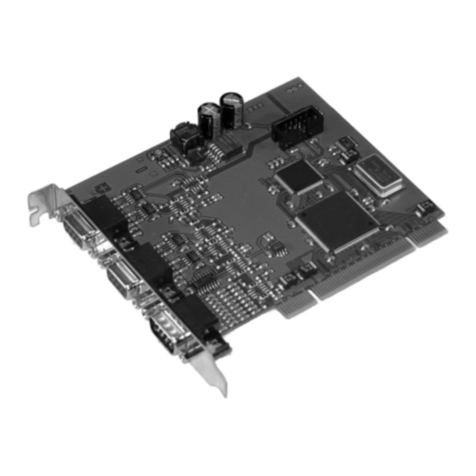
Dynamic Engineering PCIeBiSerialDb37-LM9 User manual

Embedded Solutions Page 1
DYNAMIC ENGINEERING
150 DuBois St. Suite C, Santa Cruz, CA 95060
831-457-8891 Fax 831-457-4793
http://www.dyneng.com
Est. 1988
User Manual
PCIeBiSerialDb37-LM9
ARC210 IF / Parallel Port
PCIe 4 lane Module
Transmit and Receive Interface Protocols
RS485/422
Revision A1
Corresponding Hardware: Revision 1
10-2009-0401
FLASH 0101

Embedded Solutions Page 2
PCIeBiSerialDb37LM9
ARC-210 and Digital Parallel Interface
PCIe Module
Dynamic Engineering
150 DuBois St. Suite C, Santa Cruz CA 95060
831-457-8891 831-457-4793 FAX
This document contains information of proprietary interest to Dynamic Engineering. It
has been supplied in confidence and the recipient, by accepting this material, agrees
that the subject matter will not be copied or reproduced, in whole or in part, nor its
contents revealed in any manner or to any person except to meet the purpose for which
it was delivered.
Dynamic Engineering has made every effort to ensure that this manual is accurate and
complete. Still, the company reserves the right to make improvements or changes in the
product described in this document at any time and without notice. Furthermore,
Dynamic Engineering assumes no liability arising out of the application or use of the
device described herein.
The electronic equipment described herein generates, uses, and can radiate radio
frequency energy. Operation of this equipment in a residential area is likely to cause
radio interference, in which case the user, at his own expense, will be required to take
whatever measures may be required to correct the interference.
Dynamic Engineering’s products are not authorized for use as critical components in life
support devices or systems without the express written approval of the president of
Dynamic Engineering.
This product has been designed to operate with PCIe motherboards and compatible
user-provided equipment. Connection of incompatible hardware is likely to cause
serious damage.
©2009 by Dynamic Engineering.
Other trademarks and registered trademarks are owned by their respective manufacturers.
Manual Revision A. Revised 10/9/09

Embedded Solutions Page 3
Table of Contents
PRODUCT DESCRIPTION 6
ADDRESS MAP 12
PROGRAMMING 14
Base Register Definitions 16
LM9_BASE_BASE 16
LM9_BASE_ID 17
LM9_BASE_STATUS 18
LM9_CHAN_CNTRL 19
LM9_CHAN_STATUS 21
LM9_CHAN_TX_FIFO_COUNT 26
LM9_CHAN_RD_DMA_PNTR 26
LM9_CHAN_RX_FIFO_COUNT 27
LM9_CHAN_FIFO 27
LM9_CHAN_TX_AMT_LVL 28
LM9_CHAN_RX_AFL_LVL 28
LM9_CHAN_TX 29
LM9_CHAN_TX_PACKET_LEN_FIFO 31
LM9_CHAN_TX_PACKET_LEN_REG 32
LM9_CHAN_RX 33
LM9_CHAN_RX_PACKET_LEN_FIFO 35
LM9_CHAN_RX_TIMEOUT_LEN 35
LM9_CHAN_RX_BYTECOUNT_LEN 36
LOOP-BACK 37
PCIE MODULE FRONT PANEL IO INTERFACE PIN ASSIGNMENT 38
APPLICATIONS GUIDE 39
Interfacing 39
Construction and Reliability 40
Thermal Considerations 40
Warranty and Repair 41
Service Policy 41

Embedded Solutions Page 4
Out of Warranty Repairs 41
SPECIFICATIONS 42
ORDER INFORMATION 43

Embedded Solutions Page 5
List of Figures
FIGURE 1 PCIEBISERIALDB37LM9 BLOCK DIAGRAM 7
FIGURE 2 PCIEBISERIALDB37LM9 TIMING DIAGRAM 11
FIGURE 3 PCIEBISERIALDB37LM9 INTERNAL ADDRESS MAP BASE FUNCTIONS 12
FIGURE 4 PCIEBISERIALDB37LM9 CHANNEL ADDRESS MAP 13
FIGURE 5 PCIEBISERIALDB37LM9 CONTROL BASE REGISTER BIT MAP 16
FIGURE 6 PCIEBISERIALDB37LM9 ID AND SWITCH BIT MAP 17
FIGURE 7 PCIEBISERIALDB37LM9 STATUS PORT BIT MAP 18
FIGURE 8 PCIEBISERIALDB37LM9 CHANNEL CONTROL REGISTER 19
FIGURE 9 PCIEBISERIALDB37LM9 CHANNEL STATUS PORT 21
FIGURE 10 PCIEBISERIALDB37LM9 WRITE DMA POINTER REGISTER 25
FIGURE 11 PCIEBISERIALDB37LM9 TX FIFO DATA COUNT PORT 26
FIGURE 12 PCIEBISERIALDB37LM9 READ DMA POINTER REGISTER 26
FIGURE 13 PCIEBISERIALDB37LM9 RX FIFO DATA COUNT PORT 27
FIGURE 14 PCIEBISERIALDB37LM9 RX/TX FIFO PORT 27
FIGURE 15 PCIEBISERIALDB37LM9 TX ALMOST EMPTY LEVEL REGISTER 28
FIGURE 16 PCIEBISERIALDB37LM9 RX ALMOST FULL LEVEL REGISTER 28
FIGURE 17 PCIEBISERIALDB37LM9 CHANNEL TRANSMIT CONTROL REGISTER 29
FIGURE 18 PCIEBISERIALDB37LM9 TX PACKET SIZE FIFO 31
FIGURE 19 PCIEBISERIALDB37LM9 TX PACKET SIZE REGISTER 32
FIGURE 20 PCIEBISERIALDB37LM9 CHANNEL RX CONTROL REGISTER 33
FIGURE 21 PCIEBISERIALDB37LM9 RX PACKET SIZE 35
FIGURE 22 PCIEBISERIALDB37LM9 RX TIMEOUT LENGTH 35
FIGURE 23 PCIEBISERIALDB37LM9 RX BYTECOUNT LENGTH 36
FIGURE 24 PCIEBISERIALDB37LM9 FRONT PANEL INTERFACE 38

Embedded Solutions Page 6
Product Description
In embedded systems many of the interconnections are made with differential [RS-
422/485 or LVDS] signals. Depending on the system architecture an IP, PMC or native
bus card will be the right choice to make the connection. You have choices with carriers
for cPCI, PCI, PCIe, VME, PC/104p and other buses for both PMC and IP mezzanine
modules.
The BiSerial family includes IP, PMC and PCIe versions, each with multiple “clientized”
design implementations.
Usually the choice of format is based on other system constraints. Dynamic
Engineering is happy to assist in your decision regarding architecture and other trade-
offs with the form factor decision. Dynamic Engineering has carriers for IP and PMC
modules for most systems, and is adding more as new solutions are requested by our
clients.
The PCIe compatible PCIeBiSerialDb37 has 18 independent differential IO available. A
DB-37 connector is mounted through the bezel to carry the signals. Each of the IO
have independent direction and termination controls. Each of the IO are matched
length and routed with 100 Ωdifferential impedance.
The IO are buffered from the FPGA with differential transceivers. The transceivers can
be populated with LVDS or RS-485 compatible devices. The power plane for the
transceivers is isolated to allow selectable 3.3 or 5V references for the IO. The LVDS
IO requires 3.3, and 40 MHz capable RS-485 requires 5V. When mixed LVDS and
RS485 are used the reference is set to 3.3 and lower speed RS-485 parts are used that
are compatible with the 3.3V.
Each IO has pull-up and pull-down options to allow half duplex lines to be set to a
“marking” state when no device is on the line. The P is is ganged and the M side is too.
Each side can be set to gnd or vcc to allow a ‘1’ or a ‘0’ to be set on the lines. The
resistors are in resistor packs and can be implemented with many values.
The terminations utilize analog switches to selectively parallel terminate the differential
pair with approximately 100 ohms. It is recommended that the receiver side provide the
termination.
The analog switches are protected with a DIODE on the input side of the power supply.
The switches can back-feed voltage into the rest of the circuit when powered down and
the system connected to it is not. The DIODE’s allow for more flexible operation and
power sequencing.
PcieBiSerialDb37Lm9 is a “clientized” version of the standard PCIeBiSerialDb37 board.

Embedded Solutions Page 7
“LM9” is set to use the RS485/RS422 standard, and supports one Transmit and one
Receive channel plus a parallel port. The transmitter and receiver are designed to
interface with the ARC-210 radio.
Figure 1 PCIEBISERIALDB37LM9 Block Diagram
The ARC-210 will supply the “SendTiming” and “ReceiveTiming” clock reference
signals. The PLL can be used to create a Tx clock reference to allow for loop-back
testing. The control is via SW. The PLL is referenced to 50 MHz. and can be
programmed with new .JED files using the driver.
The ARC-210 interface is serial with an interface similar to a UART. The Start and
Marking bits have opposite polarity with the Start bit being active high ‘1’ and the
marking state being a “0” on the lines. The hardware is programmable to allow the Start
bit to be active low and the marking state to be active high. Data is transferred as byte
wide with a reference clock. The reference clock is received from the radio. The default
is to use the rising edge of the reference clock with data stable on the falling edge. The
clock polarity is programmable to allow the active and stable edges to be reversed.
Parity is added with a programmable Odd or Even definition. The transmitter will assert
RTS and wait for CTS before transmitting data.

Embedded Solutions Page 8
The number of bytes to send is programmable. The number can be stored into a
secondary FIFO to allow multiple packets to be transmitted from a single larger DMA
transfer. The number of bytes can also be stored into a register to cover cases where
the size of each packet is consistent.
The hardware waits until there is a definition of the byte count, and data in the transmit
FIFO before starting. Once started if the data FIFO is empty when the transmitter is
ready to read the next data set an error for underflow is flagged. The error can cause
an interrupt if desired.
The receiver is designed to be always ready when the radio transmits data to the LM9
interface. The receiver channel when enabled can accept data from the radio
independent of the transmitter. This allows for loop-back or other applications. The
ARC-210 can only transmit or receive and not both at the same time. The receiver will
only receive data when the transmitter is not operating – in a system situation.
The receiver uses a 33 MHz clock to sample the received data and clock and to control
the data flow internally. The expected ReceiveTiming rate is around 1 MHz. leaving
plenty of headroom for the sampling and data control.
The received timing input is converted to a series of 33 MHz. pulses which are used to
enable the receive shift register to capture the synchronized Receive Data. As the data
is captured the marking state is checked to allow for initial start-up [10 bits+ of marking
bits in a row]. The state-machines check if in the marking state and then if a start bit
has been received. Data bits are counted and when a complete Start Byte Parity
sequence is received the data is parallel loaded to a holding register. Parity is
calculated and tested against what was received. The data is moved to a secondary
holding register to build up to a 32 bit word. When 4 bytes are received or at the end of
a programmed length the data is moved to the output FIFO.
Both the transmitter and receiver allow for bit and byte reversal. The data is stored as
32 bit words into the transmit FIFO from the system or the receive FIFO from the
interface. The data is used with little Endian conventions as the default – 0,1,2,3 for the
byte order where 0 = D7-0 [data on AD7-0] first and D31-24 last. The bits are sent LSB
first so D0 is first on the line and D31 is last if all 4 bytes are to be sent. Similarly the
receiver loads 0,1,2,3 so the first bit in goes into D0 and the last into D31 for each long
word. When the bytes are reversed the order becomes 3,2,1,0 which which would
make the IO 24 first, 7 last since it is still lsb first. The bit reversal swaps D7 with D0 etc
on each byte read so the order becomes D31 first and D0 last if both reversal options
are selected. For systems using Windows Little Endian is consistent with the driver and
memory mapping. With Linux and some RISC based systems the reversal may be
necessary.

Embedded Solutions Page 9
The transmitter and receiver have 4K x 32 FIFO’s with direct access, DMA support, and
loop-back capabilities. The driver/reference software includes examples of all three
modes.
DMA when used will keep the transmitter FIFO full and the receiver FIFO empty
automatically and without overflow etc. The hardware has the necessary flow control
designed in.
In addition the transmitter side has a 2K x 32 Packet FIFO where each entry stored
represents the number of bytes to send in a given transmission. RTS is held on during
a packet transmission. RTS is released between transmissions and then reasserted
and checked. CTS is not checked during the transmission since the radio is
unidirectional and has no way to receive a “pause” from the “other end”. Smaller
packets can be used for more frequent checking.
For situations where more consistent and likely shorter transmissions are to happen the
registered byte count can be used. The hardware will repeat the same size packet with
new data from the data FIFO as long as there is data in the FIFO.
Please note that the Data in the FIFO’s are packed on a Packet basis. The last LW is
padded as necessary to reach 32 bits. On the receive side the storage register is
cleared between each long word to pad with 0’s in each location not used.
Similarly the RX Packet FIFO is used to store the number if bytes in each packet
received. The RX Packet FIFO is also 2K x 32.
The receive Packet size can be determined by programming the local Packet Length
and selection of the Packet length mode or by using the timeout function and having a
variable length packet automatically received.
Custom cables can be manufactured to your requirements. The loop-back IO
definitions are toward the end of this manual. Please contact Dynamic Engineering with
your specifications.
In the “LM9” design the Termination and Direction controls are set in the VHDL for the
ARC-210 IO and programmable with software for the GPIO. The received signals are
terminated and the transmitted signals are not.
All of the IO are routed through the FPGA to allow for custom applications. Larger
external and internal FIFO’s and Dual Ported memories can be implemented with
different FPGA selections and adding the 128K x 32 FIFO’s to the board.

Embedded Solutions Page 10
The registers are mapped as 32 bit words and support 32 bit access. Most registers are
read-writeable. The Windows® and Linux compatible drivers are available to provide
the system level interface for this version of the Biserial. Use standard C/C++ to control
your hardware or use the Hardware manual to make your own software interface. The
software manuals are also available on-line.
PcieBiserialDb37 can be used for multiple purposes with applications in
telecommunications, control, sensors, IO, test; anywhere multiple independent or
coordinated IO are useful.
PcieBiserialDb37 features a Xilinx FPGA, and high speed differential devices. The
FPGA contains the PCI interface and control required for the parallel interface.
The Xilinx design incorporates the “PCI Core” and additional modules for DMA in
parallel with a direct register decoded programming model. The design model has a
“base” level with the basic board level functions and “channels” which contain IO
oriented functions. In the LM9 design the ARC-210 functions are designed into the
channel and the PLL programming, switch, GPIO and other common or basic functions
are in the base design.
From a software perspective the design can be treated as “Flat” or as a hierarchy. The
Dynamic Engineering Windows® driver uses the hierarchical approach to allow for more
consistent software with common bit maps and offsets. This implentation has only one
channel. The channel function was kept to allow for future expansion with more than 1
ARC-210 interface or a secondary function in added channels. The user software can
control the Channels with the same calls and use the channel number to distinguish.
This makes for consistent and easier to implement user level software.
The hardware is designed with each of the channels on a common address map – each
channel has the same memory allocated to it and as much as possible the offsets within
each space are defined in the same way or similar way. Again this make understanding
each port easier to accomplish and less likely to have errors.
The transceivers are initialized to the receive state. Once a channel is defined via
software to be a transmitter the IO are enabled and driven to the appropriate levels.
Terminations are activated for ports defined to be receivers.
PcieBiserialDb37 is part of the PCIe Module family of modular I/O components. The
PcieBiserialDb37 conforms to the PCIe standard. This guarantees compatibility with
your PCIe system. The base is 4 lane operation. The design can handle 1-4 lanes
being available. LED’s are provided to show the active PCIe lanes.
Designs implemented on PC104p, PMC, IP and PCIe versions of the BiSerial family can

Embedded Solutions Page 11
in large part be ported between platforms. If you see what you need in one version and
prefer it on another please contact Dynamic Engineering about porting the design. In
most cases it will require a recompile of the VHDL and not much more. We do a lot of
“just like but different “ adaptations for our clients. Please contact us to help you with a
successful special adaptation of off- the-shelf hardware.
The DMA programmable length is 32 bits => longer than most computer OS will allow in
one segment of memory. The DMA is scatter gather capable for longer lengths than the
OS max and for OS situations where the memory is not contiguous. With Windows®
lengths of 4K are common while Linux can provide much larger spaces. Larger spaces
are more efficient as there are fewer initialization reads and reduced overhead on the
bus. A single interrupt can control the entire transfer. Head to tail operation can also be
programmed with two memory spaces with two interrupts per loop.
The hardware is organized with the IO function in channel 0 and the card level functions
in the “base”. The driver provides the ability to find the hardware and to allocate
resources to use the base and channel functions.
The basic use of the interface is to facilitate data transfer via ARC-210 radio between
the host and the remote target.
Transmitter
RTS
CTS
SendTiming
Data Out 0 7 P
•••
Start Stop Stop Marking
Figure 2 PCIEBISERIALDB37LM9 Timing Diagram
Transmitter side timing is shown. The SendTiming signal is the reference clock and is
supplied by the Radio [ARC-210] and is free running. RTS is asserted when the host
has data to transmit via radio. The radio responds with CTS [or could already be
asserted]. Data is sent with a start bit, byte of data, parity and then 2 stop bits. If more
bytes are available to send, the next byte would start after the two stop bits. If no more
data then the stop bits are continued [and called marking].

Embedded Solutions Page 12
Address Map
Function Offset
// PCIeBiSerialDb37LM9 BASE definitions
#define LM9_BASE_BASE 0x0000 // 0 LM9Base Base control register
#define LM9_BASE_PLL_WRITE 0x0000 // 0 LM9Base Base control register
#define LM9_BASE_PLL_READ 0x0000 // 0 LM9Base base control register
#define LM9_BASE_USER_SWITCH 0x0004 // 1 LM9Base User DIP switch read
#define LM9_BASE_XILINX_REV 0x0004 // 1 LM9Base Xilinx revision read port
#define LM9_BASE_XILINX_DES 0x0004 // 1 LM9Base Xilinx design read port
#define LM9_BASE_STATUS 0x0008 // 2 LM9Base status Register offset
// 17-6 IO numbering, 11-0 register numbering for a 12 bit GPIO interface with an IO offset
#define LM9_BASE_GPIO_TERM 0x0040 // 16 LM9Base GPIO Termination Register offset
#define LM9_BASE_GPIO_DIR 0x0044 // 17 LM9Base GPIO Direction Register offset
#define LM9_BASE_GPIO_DATA 0x0048 // 18 LM9Base GPIO Data Register offset --
register data R/W
#define LM9_BASE_GPIO_IO 0x004C // 19 LM9Base GPIO Data IO offset (read only)
Figure 3 PCIeBiSerialDb37LM9 Internal Address Map Base Functions
The address map provided is for the local decoding performed within
PcieBiserialDb37Lm9. The addresses are all offsets from a base address. Dynamic
Engineering prefers a long-word oriented approach because it is more consistent across
platforms.
The map is presented with the #define style to allow cutting and pasting into many
compilers “include” files.
The host system will search the PCI bus to find the assets installed during power-on
initialization. The VendorId = 0x10EE and the CardId = 0x003E for the
PcieBiSerialDb37Lm9.
The LM9 design has 1 channel implemented at this time. The BASE contains the
common elements of the design, while the Channels have the IO specific interfaces.
The BASE starts at the card offset. Channel 0 starts at register 20
Section Register Address Range COM name
(starting Hex address)
Base 0-19 (0x0000) PLL, Switch, Status
Channel 0 20-39 (0x0050) ARC-210 Transmitter & Receiver

Embedded Solutions Page 13
Function Offset from Channel Base Address
// PCIeBiSerialDb37LM9 Channel definitions
#define LM9_CHAN_CNTRL 0x00000000 //0 LM9Chan General control register
#define LM9_CHAN_STATUS 0x00000004 //1 LM9Chan Interrupt status port
#define LM9_CHAN_INT_CLEAR 0x00000004 //1 LM9Chan Interrupt clear port
#define LM9_CHAN_WR_DMA_PNTR 0x00000008 //2 LM9Chan Write DMA dpr physical PCI
address register
#define LM9_CHAN_TX_FIFO_COUNT 0x00000008 //2 LM9Chan TX FIFO count read port
#define LM9_CHAN_RD_DMA_PNTR 0x0000000C //3 LM9Chan Read DMA physical PCI
address register
#define LM9_CHAN_RX_FIFO_COUNT 0x0000000C //3 LM9Chan RX FIFO count read port
including pipeline
#define LM9_CHAN_FIFO 0x00000010 //4 LM9Chan FIFO for single word RW
#define LM9_CHAN_TX_AMT_LVL 0x00000014 //5 LM9Chan TX almost empty level RW
#define LM9_CHAN_RX_AFL_LVL 0x00000018 //6 LM9Chan RX almost full level register
RW, used for HW control
#define LM9_CHAN_TX 0x0000001C //7 LM9Chan TX control register
#define LM9_CHAN_TX_PACKET_LEN_FIFO 0x00000020 //8 LM9Chan Packet Length Tx FIFO
#define LM9_CHAN_TX_PACKET_LEN_REG 0x00000024 //9 LM9Chan Packet Length Tx Register
#define LM9_CHAN_RX 0x00000034 //13 LM9Chan RX control register
#define LM9_CHAN_RX_PACKET_LEN_FIFO 0x00000038 //14 LM9Chan Packet Length Rx FIFO
#define LM9_CHAN_RX_TIMEOUT_LEN 0x0000003C //15 LM9Chan Time out between packets
#define LM9_CHAN_RX_BYTECOUNT_LEN 0x00000040 //16 LM9Chan Byte Count length expected
Figure 4 PcieBiSerialDb37Lm9 Channel Address Map

Embedded Solutions Page 14
Programming
Programming the PcieBiSerialDb37Lm9 requires only the ability to read and write data
in the host's PCIe space.
Once the initialization process has occurred, and the system has assigned addresses to
the PcieBiSerialDb37Lm9 card the software will need to determine what the address
space is for the PCI interface [BAR0]. The offsets in the address tables are relative to
the system assigned BAR0 base address.
The next step is to initialize the PcieBiSerialDb37Lm9. The PLL will need to be
programmed to use the loop-back function. The Cypress CyberClocks software can be
used to create new .JED files if desired. PLLA should be set to the transmit reference
frequency output by the transmitter.
The driver comes with a .JED file prepared. The driver has a utility to load the PLL and
read back. The reference application software has an example of the use of PLL
programming. The reference application software also includes XLATE.c which
converts the .JED file from the CyberClocks tool to an array that can be programmed
into the PLL.
The IO for the ARC-210 direction and termination are hardwired in this design. The
ports are unidirectional and initialization is simplified with this approach. The GPIO
ports can be programmed if used. The termination should be set for any input bits
[unless the termination is located in your cable] and any transmitters will need to be
enabled.
The control bits for the ARC-210 will select how the data is transmitted – Byte ordering,
size of transfer etc.
For Windows™ and Linux systems the Dynamic Drivers can be used. The driver will
take care of finding the hardware and provide an easy to use mechanism to program
the hardware. The Driver comes with reference software showing how to use the card
and reference frequency files to allow the user to duplicate the test set-up used in
manufacturing at Dynamic Engineering. Using simple, known to work routines is a good
way to get acquainted with new hardware.
To use the LM9 specific functions the Channel Control, and PLL interface plus DMA will
need to be programmed. To use DMA, memory space from the system should be
allocated and the link list stored into memory. The location of the link list is written to
the LM9 to start the DMA. Please refer to the Burst IN and Burst Out register
discussions.

Embedded Solutions Page 15
DMA should be set-up before starting the channel port function. For transmission this
will result in the FIFO being full or close to it when the transfer is started or at least the
Packet loaded if shorter than the FIFO size. For reception it means that the FIFO is
under HW control and the delay from starting reception to starting DMA won’t cause an
overflow condition.
DMA can be programmed with a specific length. The length can be as long as you want
within standard memory limitations. At the end of the DMA transfer the Host will receive
an interrupt. The receiver can be stopped and the FIFO reset to clear out any extra
data captured. For on-the-fly processing multiple shorter DMA segments can be
programmed; at the interrupt restart DMA to point at the alternate segment to allow
processing on the previous one. This technique is sometimes referred to as “ping-
pong”.
The Receive Byte Count register can be used to control the input Packet size to work
with your DMA scheme. Alternately the Byte Count register can be programmed to the
size of the Packet if known. For situations where the size is unknown the timeout and
Almost Full interrupt options can be used.
Please see the channel control register bit maps for more information.

Embedded Solutions Page 16
Base Register Definitions
LM9_BASE_BASE
[$00 Base Control Register Port read/write]
DATA BIT DESCRIPTION
31-21 spare
20 bit 19 read-back of pll_dat register bit
19 pll_dat [write to PLL, read-back from PLL]
18 pll_s2
17 pll_sclk
16 pll_en
15-0 spare
Figure 5 PcieBiSerialDb37Lm9 Control Base Register Bit Map
This is the base control register for the LM9. The features common to all channels are
controlled from this port. Unused bits are reserved for additional new features. Unused
bits should be programmed ‘0’ to allow for future commonality.
pll_en: When this bit is set to a one, the signals used to program and read the PLL are
enabled.
pll_sclk/pll_dat : These signals are used to program the PLL over the I2C serial
interface. Sclk is always an output whereas Sdata is bi-directional. This register is
where the Sdata output value is specified or read-back.
pll_s2: This is an additional control line to the PLL that can be used to select additional
pre-programmed frequencies. Set to ‘0’ for most applications.
The PLL is programmed with the output file generated by the Cypress PLL
programming tool. [CY3672 R3.01 Programming Kit or CyberClocks R3.20.00 Cypress
may update the revision from time to time.] The .JED file is used by the Dynamic Driver
to program the PLL. Programming the PLL is fairly involved and beyond the scope of
this manual. For clients writing their own drivers it is suggested to get the Engineering
Kit for this board including software, and to use the translation and programming files
ported to your environment. This procedure will save you a lot of time. For those who
want to do it themselves the Cypress PLL in use is the 22393. The output file from the
Cypress tool can be passed directly to the Dynamic Driver [Linux or Windows] and used
to program the PLL without user intervention.

Embedded Solutions Page 17
The reference frequency for the PLL is 50 MHz.
LM9_BASE_ID
[$04 Switch and Design number port read only]
DATA BIT DESCRIPTION
31-24 spare
23-8 Design ID and Revision
7-0 DIP switch
Figure 6 PcieBiSerialDb37Lm9 ID and Switch Bit Map
The DIP Switch is labeled for bit number and ‘1’ ‘0’ in the silk screen. The DIP Switch
can be read from this port and used to determine which PcieBiserialDb37Lm9 physical
card matches each PCI address assigned in a system with multiple cards installed.
The DIPswitch can also be used for other purposes – software revision etc. The switch
shown would read back 0x12.
The Design ID and Revision are defined by a 16 bit field allowing for 256 designs and
256 revisions of each. The LM9 design is 0x01 the current revision is 0x01.
The PCI revision is updated in HW to match the design revision. The board ID will be
updated for major changes to allow drivers to differentiate between revisions and
applications.
1
7 0
0

Embedded Solutions Page 18
LM9_BASE_STATUS
[$08 Board level Status Port read only]
DATA BIT DESCRIPTION
31-10 set to ‘0
9 undefined
8 undefined
7-1 set to ‘0’, reserved for additional channels
0 Unmasked Ch0 Interrupt
Figure 7 PcieBiSerialDb37Lm9 Status Port Bit Map
Channel Interrupt – The local interrupt status from the channel. Each channel can
have different interrupt sources. DMA Write or DMA Read or IntForce or TX/RX request
are typical sources. Polling can be accomplished using the channel status register and
leaving the channel interrupt disabled.

Embedded Solutions Page 19
Channel Bit Maps
The LM9 design has 1 channel. The basic control signals are the same for the channel
base, channel status, FIFO and DMA interfaces across multiple designs.
Notes:
The offsets shown are relative to the channel base address not the card base address.
LM9_CHAN_CNTRL
[0x0] Channel Control Register (read/write)
Channel Control Register
Data Bit Description
31-7 spare
12 reserved this design FIFO External Reset
11-9 Spare
8 OutUrgent
7 InUrgent
6 Read DMA Interrupt Enable
5 Write DMA Interrupt Enable
4 Force Interrupt
3 Channel Interrupt Enable
2 Bypass
1 Receive FIFO Reset
0 Transmit FIFO Reset
Figure 8 PcieBiSerialDb37Lm9 channel Control Register
FIFO Transmitter/Receiver Reset: When set to a one, the transmit and/or receive FIFOs
will be reset. When these bits are zero, normal FIFO operation is enabled. In addition
the Transmit and Receive State Machines are also reset.
Write/Read DMA Interrupt Enable: These two bits, when set to one, enable the
interrupts for DMA writes and reads respectively.
Channel Interrupt Enable: When this bit is set to a one, all enabled interrupts (except
the DMA interrupts) will be gated through to the PCI interface level of the design; when
this bit is a zero, the interrupts can be used for status without interrupting the host. The
channel interrupt enable is for the channel level interrupt sources only.

Embedded Solutions Page 20
Force Interrupt: When this bit is set to a one, a system interrupt will occur provided the
Channel Interrupt enable is set. This is useful for interrupt testing.
InUrgent / OutUrgent when set causes the DMA request to have higher priority under
certain circumstances. Basically when the TX FIFO is almost empty and InUrgent is set
the TX DMA will have higher priority than it would otherwise get. Similarly if the RX
FIFO is almost full and OutUrgent is set the read DMA will have higher priority. The
purpose is to allow software some control over how DMA requests are processed and to
allow for a higher rate channel to have a higher priority over other lower rate channels.
ByPass when set allows the FIFO to be used in a loop-back mode internal to the device.
A separate state-machine is enabled when ByPass is set and the TX and RX are not
enabled. The state-machine checks the TX and RX FIFO’s and when not empty on the
TX side and not Full on the RX side moves data between them. Writing to the TX FIFO
allows reading back from the RX side. An example of this is included in the Driver
reference software.
FIFO External Reset: When cleared to a zero, the External FIFOs will be reset. When
set the External FIFO is enabled. Please note that the state of the Load pin in the
transmit control register affects how the part comes out of reset – what the default
Almost Full and Almost Empty offsets are.
This function is reserved since the LM9 design does not use external FIFO’s.
Table of contents
Other Dynamic Engineering PCI Card manuals

Dynamic Engineering
Dynamic Engineering SpaceWire BK User manual

Dynamic Engineering
Dynamic Engineering PCIe8LSwVPX3U User manual

Dynamic Engineering
Dynamic Engineering LVDS 8R User manual

Dynamic Engineering
Dynamic Engineering PCIe 8L XMC X1 User manual

Dynamic Engineering
Dynamic Engineering PCIe8LXMCX2CB User manual

Dynamic Engineering
Dynamic Engineering cPCIBPMC6U User manual

Dynamic Engineering
Dynamic Engineering PCI2PMC User manual

Dynamic Engineering
Dynamic Engineering PC104p-SpaceWire-Monitor User manual