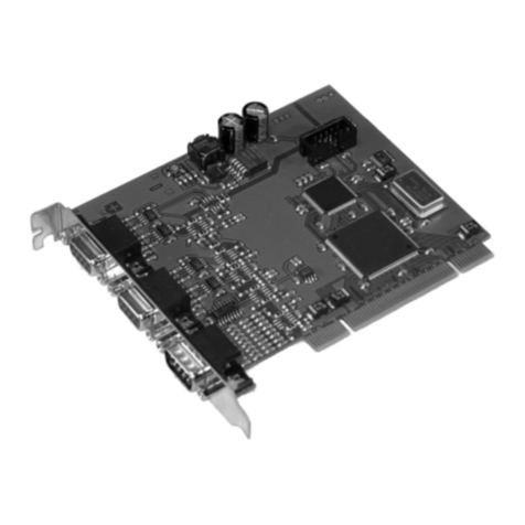
Dynamic Engineering cPCIBPMC6U User manual

DYNAMIC ENGINEERING
150 DuBois St. Suite B/C Santa Cruz CA 95060
831-457-8891
https://www.dyneng.com
Est. 1988
User Manual
cPCIBPMC6U
cPCI 6U 4HP 2 Position PMC Compatible Carrier
Previous model with shown
Manual Revision 10p1 6/9/22
Corresponding Hardware: Revision 10
Fab number: 10-2006-0710

Embedded Solutions Page
2
cPCIBPMC6U
cPCI and PMC Compatible Carrier
Dynamic Engineering
150 DuBois St Suite B/C
Santa Cruz, CA 95060
831-457-8891
This document contains information of
proprietary interest to Dynamic Engineering. It
has been supplied in confidence and the
recipient, by accepting this material, agrees that
the subject matter will not be copied or
reproduced, in whole or in part, nor its contents
revealed in any manner or to any person except
to meet the purpose for which it was delivered.
Dynamic Engineering has made every effort to
ensure that this manual is accurate and
complete. Still, the company reserves the right to
make improvements or changes in the product
described in this document at any time and
without notice. Furthermore, Dynamic
Engineering assumes no liability arising out of
the application or use of the device described
herein.
The electronic equipment described herein
generates, uses, and can radiate radio
frequency energy. Operation of this equipment
in a residential area is likely to cause radio
interference, in which case the user, at his own
expense, will be required to take whatever
measures may be required to correct the
interference.
Dynamic Engineering’s products are not
authorized for use as critical components in life
support devices or systems without the express
written approval of the president of Dynamic
Engineering.
Connection of incompatible hardware is likely to
cause serious damage.
© by Dynamic Engineering.
Other trademarks and registered trademarks are owned by their
respective manufactures.

Embedded Solutions Page
3
PRODUCT DESCRIPTION 5
DIP SWITCH Settings 6
SW1 DIP SWITCH Settings 6
Interrupts 7
Options 7
Other Signals 7
Other Options 8
PMC Position 0 Rear Panel IO Interface Pin Assignment 9
PMC Position 1 Rear Panel IO Interface Pin Assignment 10
APPLICATIONS GUIDE 11
Interfacing 11
Construction and Reliability 12
Thermal Considerations 12
WARRANTY AND REPAIR 13
Service Policy 13
Out of Warranty Repairs 13
For Service Contact: 13
SPECIFICATIONS 14
ORDER INFORMATION 15

Embedded Solutions Page
4
FIGURE 1 CPCIBPMC6U POSITION O PN4 INTERFACE STANDARD 9
FIGURE 2 CPCIBPMC6U POSITION 1 PN4 INTERFACE STANDARD 10

Embedded Solutions Page
5
Product Description
cPCIBPMC6U is part of the Dynamic Engineering cPCI and PMC Compatible
family of modular I/O components. cPCIBPMC6U adapts two PMC modules into
one cPCI slot.
cPCIBPMC6U has a “sister” product for 3U applications – cPCIBPMC3U32. The
3U version has a 32 bit PCI interface definition and can work in a 64 bit
environment.
Voltages are monitored and the associated LEDs illuminated when the
corresponding voltages are within tolerance.
5V and 3.3V power planes are filtered through an LC network. 1A per pin on the
3.3 and 5V planes [more than 10A each], plus 1A+ on the +/- 12V connections.
Special features:
• Universal cPCI 6U 4HP.
• Extended temperature range [-40 +85C] components
LED names within quotes: (visible on bezel)
• LED on PMC Busmode “LPMC0” & “LPMC1”
• LED on plus 12V “L12V”
• LED on minus 12V “LM12V”
• LED on plus 5V “L5V”
• LED on plus 3.3V “L3p3V”
• User selectable secondary VIO.
• 32 bit operation on PCI bus
• 66 or 33 MHz operation. With 66 MHz. primary bus speed the secondary bus
can be 66 or 33 MHz.
• Front panel connector access through cPCI bracket
• JTAG programming support option for position 0
• GPIO header option
• Rear Panel IO option
cPCIBPMC6U is ready to use with the default settings. Just install the PMC(s)
onto cPCIBPMC6U and into the system. There are a few settings to optimize
performance.

Embedded Solutions Page
6
DIP SWITCH Settings
Please note that the switch numbering and ’CLOSED’ and ‘0PEN’ definitions are
per the silk-screen. Closed corresponds to ‘0’ and open to ‘1’.
SW1 DIP SWITCH Settings
DIPSWITCH #1 [SW1 table on silk-screen]
Switch #1 selects the secondary side VIO [SVIO]. When the switch = ‘open’
3.3V is selected for the secondary side. When ‘closed’ is selected 5V is the VIO
definition. The VIO plane is a reference for the IO level. The specification does
not prohibit larger current consumption from these pins. The cPCIBPMC6U
design utilizes a MOSFET to control the 5V or 3.3V rails onto the VIO plane.
Max consumption on the VIO rail is 3A. The factory setting is ‘Open’.
Switch #2 SM66EN signal is also routed to the PMC connector pin M66EN. If
the PMC uses the M66EN as an input the dipswitch can be used to control the
frequency. If the PMC uses the M66EN pin as a control, the Switch may have no
effect. For example, if the switch is in the ‘open’ position and the PMC is
selecting M66EN = ‘0’ the PMC will “win” and the signal will be at the 33 MHz
setting. Both the dipswitch and the PMC M66EN have to be enabled for 66 MHz.
.
Switch #3 Config66 is controlled with this switch. Closed selects 33 MHz and
open selects 66 MHz capable.
Switch #4 Spare
Switch #5 Spare
Switch #6 Spare
Switch #7 selects PMC Monarch Mode. For prPMCs using the Monarch Mode
pin, closing the switch will cause the Monarch Pin [64] at the PMC to be tied
through a 1KΩ resistor to ground. With the switch open the Monarch pin is tied
to 3.3V through 4.7KΩ. The factory setting is ‘Closed’.
Switch #8 is spare

Embedded Solutions Page
7
Interrupts
Interrupts from the PMCs are connected from the PMC to the primary PCI bus.
INTA - INTD are mapped directly to the primary bus segment for position 0 and
“rotated” B, C, D, A for position 1.
cPCI Position 0 Position 1
INTA INTA INTB
INTB INTB INTC
INTC INTC INTD
INTD INTD INTA
Options
Dynamic Engineering offers options to the cPCIBPMC6U design.
When -RIO is added to the part number the rear IO option is installed [J04, J14,
J3, J5]. Routing between J3 ó J04 & J5 ó J14 provides the connection. The
routing is controlled impedance, and matched length. Routed as differential parts
with 100 ohm impedance for each pair.
Fans can be added where high power PMCs are used or inadequate in chassis
circulation is present.
JTAG support is available. The JTAG header position is clearly marked in the
silk screen. The header is frequently not used and is not installed unless
requested.
The Bridge supports a GPIO function. A header position is available with the
positions clearly marked in the silk-screen. The header is installed by request.
Please contact Dynamic Engineering for this option. The 4 bits are terminated
with 4.7KΩ to 3.3V.
Other Signals
PME is pulled up with a 10K ohm resistor to 3.3V.
Reset Out on PMC position is open.

Embedded Solutions Page
8
Other Options
Dynamic Engineering offers multiple versions of the cPCIxPMC design.
cPCI2PMC is a passive implementation. The cPCI connections on the
cPCI2PMC are longer, and can limit the number of cards or adapters on a
particular bus segment. The passive design has “0” delay between the primary
PCI bus and the PMC. The VIO and bus speed definitions are common to the
primary PCI bus and PMC. This design is versatile with PCI 32, PCI 64, rear IO
versions and a slot zero configuration.
cPCIBPMC3U32 is bridged, isolating the PMC from the cPCI bus. cPCI
connections are specification compliant on cPCIBPMC3U32. cPCIBPMC3U32
can be used in multiple positions on the same PCI bus segment. The bridged
design has pipeline delays between the primary and PMC buses. The bridged
design has independent VIO definitions between the PMC and the primary bus.
This design (cPCIBPMC6U) is the 6U 2 PMC position variant.
All optional signals can be isolated or added with resistors located to create short
stubs when the signals are not in use.

Embedded Solutions Page
9
PMC Position 0 Rear Panel IO Interface Pin Assignment
Slot 0 PMC J3 PIM connection if Dual Carrier utilized
PMC_0_IO1 J3.E13 J14.1
PMC_0_IO2 J3.D13 J14.2
PMC_0_IO3 J3.C13 J14.3
PMC_0_IO4 J3.B13 J14.4
PMC_0_IO5 J3.A13 J14.5
PMC_0_IO6 J3.E12 J14.6
PMC_0_IO7 J3.D12 J14.7
PMC_0_IO8 J3.C12 J14.8
PMC_0_IO9 J3.B12 J14.9
PMC_0_IO10 J3.A12 J14.10
PMC_0_IO11 J3.E11 J14.11
PMC_0_IO12 J3.D11 J14.12
PMC_0_IO13 J3.C11 J14.13
PMC_0_IO14 J3.B11 J14.14
PMC_0_IO15 J3.A11 J14.15
PMC_0_IO16 J3.E10 J14.16
PMC_0_IO17 J3.D10 J14.17
PMC_0_IO18 J3.C10 J14.18
PMC_0_IO19 J3.B10 J14.19
PMC_0_IO20 J3.A10 J14.20
PMC_0_IO21 J3.E9 J14.21
PMC_0_IO22 J3.D9 J14.22
PMC_0_IO23 J3.C9 J14.23
PMC_0_IO24 J3.B9 J14.24
PMC_0_IO25 J3.A9 J14.25
PMC_0_IO26 J3.E8 J14.26
PMC_0_IO27 J3.D8 J14.27
PMC_0_IO28 J3.C8 J14.28
PMC_0_IO29 J3.B8 J14.29
PMC_0_IO30 J3.A8 J14.30
PMC_0_IO31 J3.E7 J14.31
PMC_0_IO32 J3.D7 J14.32
PMC_0_IO33 J3.C7 J14.33
PMC_0_IO34 J3.B7 J14.34
PMC_0_IO35 J3.A7 J14.35
PMC_0_IO36 J3.E6 J14.36
PMC_0_IO37 J3.D6 J14.37
PMC_0_IO38 J3.C6 J14.38
PMC_0_IO39 J3.B6 J14.39
PMC_0_IO40 J3.A6 J14.40
PMC_0_IO41 J3.E5 J14.41
PMC_0_IO42 J3.D5 J14.42
PMC_0_IO43 J3.C5 J14.43
PMC_0_IO44 J3.B5 J14.44
PMC_0_IO45 J3.A5 J14.45
PMC_0_IO46 J3.E4 J14.46
PMC_0_IO47 J3.D4 J14.47
PMC_0_IO48 J3.C4 J14.48
PMC_0_IO49 J3.B4 J14.49
PMC_0_IO50 J3.A4 J14.50
PMC_0_IO51 J3.E3 J14.51
PMC_0_IO52 J3.D3 J14.52
PMC_0_IO53 J3.C3 J14.53
PMC_0_IO54 J3.B3 J14.54
PMC_0_IO55 J3.A3 J14.55
PMC_0_IO56 J3.E2 J14.56
PMC_0_IO57 J3.D2 J14.57
PMC_0_IO58 J3.C2 J14.58
PMC_0_IO59 J3.B2 J14.59
PMC_0_IO60 J3.A2 J14.60
PMC_0_IO61 J3.E1 J14.61
PMC_0_IO62 J3.D1 J14.62
PMC_0_IO63 J3.C1 J14.63
PMC_0_IO64 J3.B1 J14.64
FIGURE 1 CPCIBPMC6U POSITION O PN4 INTERFACE STANDARD

Embedded Solutions Page
10
PMC Position 1 Rear Panel IO Interface Pin Assignment
Slot 1 PMC J5 PIM connection if Dual Carrier utilized
PMC_1_IO1 J5.E13 J24.1
PMC_1_IO2 J5.D13 J24.2
PMC_1_IO3 J5.C13 J24.3
PMC_1_IO4 J5.B13 J24.4
PMC_1_IO5 J5.A13 J24.5
PMC_1_IO6 J5.E12 J24.6
PMC_1_IO7 J5.D12 J24.7
PMC_1_IO8 J5.C12 J24.8
PMC_1_IO9 J5.B12 J24.9
PMC_1_IO10 J5.A12 J24.10
PMC_1_IO11 J5.E11 J24.11
PMC_1_IO12 J5.D11 J24.12
PMC_1_IO13 J5.C11 J24.13
PMC_1_IO14 J5.B11 J24.14
PMC_1_IO15 J5.A11 J24.15
PMC_1_IO16 J5.E10 J24.16
PMC_1_IO17 J5.D10 J24.17
PMC_1_IO18 J5.C10 J24.18
PMC_1_IO19 J5.B10 J24.19
PMC_1_IO20 J5.A10 J24.20
PMC_1_IO21 J5.E9 J24.21
PMC_1_IO22 J5.D9 J24.22
PMC_1_IO23 J5.C9 J24.23
PMC_1_IO24 J5.B9 J24.24
PMC_1_IO25 J5.A9 J24.25
PMC_1_IO26 J5.E8 J24.26
PMC_1_IO27 J5.D8 J24.27
PMC_1_IO28 J5.C8 J24.28
PMC_1_IO29 J5.B8 J24.29
PMC_1_IO30 J5.A8 J24.30
PMC_1_IO31 J5.E7 J24.31
PMC_1_IO32 J5.D7 J24.32
PMC_1_IO33 J5.C7 J24.33
PMC_1_IO34 J5.B7 J24.34
PMC_1_IO35 J5.A7 J24.35
PMC_1_IO36 J5.E6 J24.36
PMC_1_IO37 J5.D6 J24.37
PMC_1_IO38 J5.C6 J24.38
PMC_1_IO39 J5.B6 J24.39
PMC_1_IO40 J5.A6 J24.40
PMC_1_IO41 J5.E5 J24.41
PMC_1_IO42 J5.D5 J24.42
PMC_1_IO43 J5.C5 J24.43
PMC_1_IO44 J5.B5 J24.44
PMC_1_IO45 J5.A5 J24.45
PMC_1_IO46 J5.E4 J24.46
PMC_1_IO47 J5.D4 J24.47
PMC_1_IO48 J5.C4 J24.48
PMC_1_IO49 J5.B4 J24.49
PMC_1_IO50 J5.A4 J24.50
PMC_1_IO51 J5.E3 J24.51
PMC_1_IO52 J5.D3 J24.52
PMC_1_IO53 J5.C3 J24.53
PMC_1_IO54 J5.B3 J24.54
PMC_1_IO55 J5.A3 J24.55
PMC_1_IO56 J5.E2 J24.56
PMC_1_IO57 J5.D2 J24.57
PMC_1_IO58 J5.C2 J24.58
PMC_1_IO59 J5.B2 J24.59
PMC_1_IO60 J5.A2 J24.60
PMC_1_IO61 J5.E1 J24.61
PMC_1_IO62 J5.D1 J24.62
PMC_1_IO63 J5.C1 J24.63
PMC_1_IO64 J5.B1 J24.64
FIGURE 2 CPCIBPMC6U POSITION 1 PN4 INTERFACE STANDARD
In the tables above Slot 0 PMC / J3 & Slot 1 PMC / J5 are part of the
cPCIBPMC6U design.
Table of contents
Other Dynamic Engineering PCI Card manuals
Dynamic Engineering
Dynamic Engineering SpaceWire BK User manual
Dynamic Engineering
Dynamic Engineering PCIe8LSwVPX3U User manual

Dynamic Engineering
Dynamic Engineering LVDS 8R User manual
Dynamic Engineering
Dynamic Engineering PCI2PMC User manual
Dynamic Engineering
Dynamic Engineering PCIe8LXMCX2CB User manual

Dynamic Engineering
Dynamic Engineering PC104p-SpaceWire-Monitor User manual
Dynamic Engineering
Dynamic Engineering PCIeBiSerialDb37-LM9 User manual
Dynamic Engineering
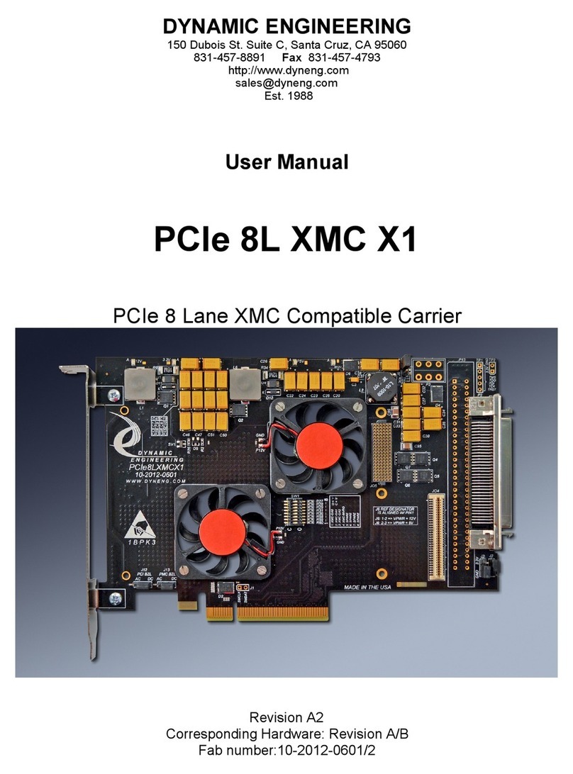
Dynamic Engineering PCIe 8L XMC X1 User manual
