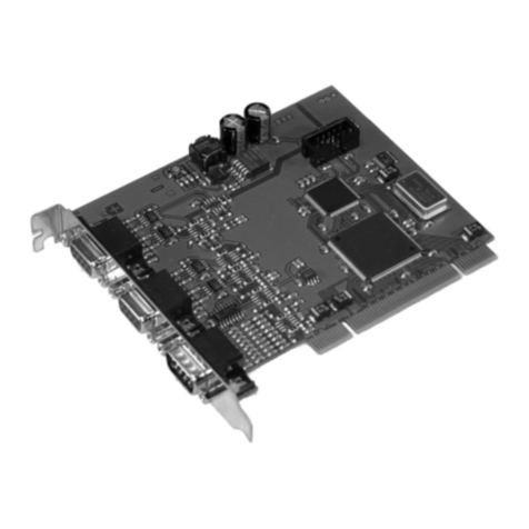
Dynamic Engineering LVDS 8R User manual

Hardware and Software Design • Manufacturing Services
page 1
PCI LVDS 8R
8 Channel LVDS Serial Interface
Dynamic Engineering
435 Park Drive, Ben Lomond, CA 95005
831-336-8891
www.dyneng.com
10-2001-0202
This document contains information of proprietary interest to Dynamic Engineering. It has been supplied in
confidence and the recipient, by accepting this material, agrees that the subject matter will not be copied or
reproduced, in whole or in part, nor its contents revealed in any manner or to any person except to meet the
purpose for which it was delivered.
Dynamic Engineering has made every effort to ensure that this manual is accurate and complete. Still, the
company reserves the right to make improvements or changes in the product described in this document at any
time and without notice. Furthermore, Dynamic Engineering assumes no liability arising out of the application or
use of the device described herein.
The electronic equipment described herein generates, uses, and can radiate radio frequency energy. Operation of
this equipment in a residential area is likely to cause radio interference, in which case the user, at his own
expense, will be required to take whatever measures may be required to correct the interference.
Dynamic Engineering’s products are not authorized for use as critical components in life support devices or
systems without the express written approval of the president of Dynamic Engineering.
This product has been designed to operate with PCI and compatible user-provided equipment. Connection of
incompatible hardware is likely to cause serious damage.
©2000,2001,2002 by Dynamic Engineering.
Manual Revision E. Revised 4/4/02

Hardware and Software Design • Manufacturing Services
page 2
Table of Contents
Introduction 4
Memory Map 7
DMA Definitions 13
DMA Base Control 13
DMA Status 16
DMA FIFO Holding Register Target Read 17
DMA FIFO Holding Register DMA Read 18
DMA Xilinx Status 19
Address Generator Definitions 20
Address Generator SDRAM Start Address Registers 20
Address Generator SDRAM Length Registers 21
Address Generator SDRAM Control Registers 22
Address Generator SDRAM Base Control Registers 25
Address Generator SDRAM Status Registers 27
FE Definitions 29
FE Tag Bit Definition Registers 29
FE X Stop Registers 32
FE Y Stop Registers 32
FE Z Stop Registers 33
FE X Total Counter Read-back 33
FE Data Holding Register 34
FE Data Write Register 34
FE Channel Done 35
FE Pre-load Counter 36

Hardware and Software Design • Manufacturing Services
page 3
Operational Brief: 37
LVDS Connector Definition 40
Construction and Reliability 43
Thermal Considerations 43
Warranty and Repair 43
Service Policy 44
Out of Warranty Repairs 44
For Service Contact: 44
Specifications 45
Order Information 46

Hardware and Software Design • Manufacturing Services
page 4
Introduction
The PCI_LVDS_8R features 8 channels of LVDS input. Each input channel is composed of 3 serial data pairs plus a
reference clock. The reference clock can operate at speeds up to 175 MHz. The National DS90CR218 [TIA/EIA-
644] or equivalent receiver chip is used. The receiver converts the three parallel streams into 21 bit parallel
data. The PCI_LVDS_8R implements the lower two serial streams for a 14 bit parallel interface. The upper serial
stream and corresponding upper 7 bits are defined and routed to allow for future expansion and alternate
protocols to be implemented.
The LVDS channels are grouped two per Front End [FE] Xilinx. The FE Xilinx receives the data and performs data
filtering to allow programmed patterns to start capture and other patterns to be stored. The Data width is built
up from 14 to 16 bits with the addition of parity. The data samples are combined to form 32 bit words before
being written to the Input FIFO. There is one Input FIFO per LVDS channel. 1K x 32.
One Latch Xilinx handles 4 LVDS channels – the output from two FE Xilinx. The data is read from the Input FIFO by
the Latch Xilinx and either written to the SDRAM or to the Output FIFO. The data is read into the Latch Xilinx at 66
MHz and written to the SDRAM at 33 MHz. The data width is doubled from 32 bits to 64 bits in this path. The
Data can also be read from the SDRAM and written to the Output FIFO. When data is written to the Output FIFO
the width is 32 bits and the rate is 66 MHz. The Address Generator controls the Latch Xilinx and the SDRAM.
The data from the output FIFO can be read directly or as a DMA stream.
The Address Generator is used to control the Latch Xilinx [data path], and provide the address control for the
SDRAM. After Power-Up the Address Generator provides the control words to the SDRAM to initialize operation
and then the proper control sequences for refresh and burst access. In Capture mode the Address Generator
polls the Input FIFOs for data to be transferred into the SDRAM. When a FIFO’s Half-Full flag is set, data is
transferred from the FIFO through the Latch Xilinx into the SDRAM. In Retrieve mode the data is read from the
SDRAM and loaded into the Output FIFO. The Output FIFO is polled to see if there is room for the next burst of
data. In Direct mode the data is moved from the Input FIFO through the Latch Xilinx to the Output FIFO without
using the SDRAM.


Hardware and Software Design • Manufacturing Services
page 5
The Data in the Output FIFO passes through the DMA Xilinx before the PLX [PCI interface] has access. The data is
written into the Output FIFO at 66 MHz and read out at 33 Mhz. The interface supports DMA and target reads.
The 2:1 load to read bandwidth insures rapid and efficient data transfer in Retrieve mode.
The FE design includes a software write path and load register to allow the software to load data words into the
Input FIFO directly. The FE design also has a 12 bit counter that can be used to load data automatically into the
FIFO for performance testing. The Counter inserts data at 33MHz. into the data path to provide a continuous data
stream. The counter can be used to cause Direct or Capture mode operations. Retrieve can be used after
capture to read the data back for test and development purposes.
The hardware as of this revision has all Channels and all data paths tested. An 8 channel LVDS data simulator was
used with multiple patterns, speeds, and programming scenarios to check on all modes of operation.

Hardware and Software Design • Manufacturing Services
page 6
LVDS IF
LVDS IF
LVDS IF
LVDS IF
FIFO
FIFO
FIFO
FIFO
SDRAM
64
32
256 MB
1K x 32
DMA Xilinx
Add Gen
Xilinx
LVDS IF
LVDS IF
LVDS IF
LVDS IF
SDRAM
32
1K x 32
LAT Xilinx
256 MB
LVDS IF
LVDS IF
LVDS IF
LVDS IF
FIFO
FIFO
FIFO
FIFO
SDRAM
64
FIFO
32
256 MB
Add Gen
Xilinx
LVDS IF
LVDS IF
SDRAM
64
32
256 MB
1K x 32
PLX 9054
PCI 33/32
FIFO
FE Xilinx
FE Xilinx
FE Xilinx
FE Xilinx
LAT Xilinx
Control Bus

Hardware and Software Design • Manufacturing Services
page 7
Memory Map
(Addresses shown as byte)
Addresses are offsets from the PCI Base Address defined by the system and the PLX 9054. The PLX 9054
requests several BARs. The BAR associated with Space 0 is the base address for the internal PCI_LVDS_8R
hardware. The CardId = 9054. The VendorId = 10B5. The Local Space must be enabled by writing a 0x0001 to
Space_0_Base [PLX 9054 internal register]. The Interrupt must be enabled within the PLX for the interrupts
described within this document to reach the host. Please download the PLX 9054 manual for complete details.
Front End Filter Channels 0,1
Decode number Address offset Chip Definition
0 0000 FE01 TAG_DEF_0
0004 FE01 X0_STOP
0008 FE01 X1_STOP
000C FE01 Y0_STOP
0010 FE01 Y1_STOP
0014 FE01 Z0_STOP
0018 FE01 Z1_STOP
001C FE01 X_TOTAL_0_RDBK
0020 FE01 X_TOTAL_1_RDBK
0024 FE01 0,1_DTA_PAT
0028 FE01 FIFO_0 WRT
002C FE01 FIFO_1 WRT
0030 FE01 TAG_DEF_1
0034 FE01 FE_DONE_0
0038 FE01 FE_DONE_1
003C FE01 Preload data counter 0-1

Hardware and Software Design • Manufacturing Services
page 8
Front End Filter Channels 2,3
Decode number Address offset Chip Definition
1 0040 FE23 TAG_DEF_2
0044 FE23 X2_STOP
0048 FE23 X3_STOP
004C FE23 Y2_STOP
0050 FE23 Y3_STOP
0054 FE23 Z2_STOP
0058 FE23 Z3_STOP
005C FE23 X_TOTAL_2_RDBK
0060 FE23 X_TOTAL_3_RDBK
0064 FE23 2,3_DTA_PAT
0068 FE23 FIFO_2 WRT
006C FE23 FIFO_3 WRT
0070 FE23 TAG_DEF_3
0074 FE23 FE_DONE_2
0078 FE23 FE_DONE_3
007C FE23 Preload data counter 2-3

Hardware and Software Design • Manufacturing Services
page 9
Address Generator Channels 0-3
Decode number Address offset Chip Definition
2 0080 ADD0_3 Start ADD CH 0
0084 ADD0_3 Start ADD CH 1
0088 ADD0_3 Start ADD CH 2
008C ADD0_3 Start ADD CH 3
0090 ADD0_3 Length CH 0
0094 ADD0_3 Length CH 1
0098 ADD0_3 Length CH 2
009C ADD0_3 Length CH 3
00A0 ADD0_3 CNTL CH 0
00A4 ADD0_3 CNTL CH 1
00A8 ADD0_3 CNTL CH 2
00AC ADD0_3 CNTL CH 3
00B0 ADD0_3 SDRAM Base 0-3
00B4-00B8 ADD0_3 Spare
00BC ADD0_3 Status 0-3
3 spare

Hardware and Software Design • Manufacturing Services
page 10
Front End Filter Channels 4,5
Decode number Address offset Chip Definition
4 0100 FE45 TAG_DEF_4
0104 FE45 X4_STOP
0108 FE45 X5_STOP
010C FE45 Y4_STOP
0110 FE45 Y5_STOP
0114 FE45 Z4_STOP
0118 FE45 Z5_STOP
011C FE45 X_TOTAL_4_RDBK
0120 FE45 X_TOTAL_5_RDBK
0124 FE45 4,5_DTA_PAT
0128 FE45 FIFO_4 WRT
012C FE45 FIFO_5 WRT
0130 FE45 TAG_DEF_5
0134 FE45 FE_DONE_4
0138 FE45 FE_DONE_5
013C FE45 Preload data counter 4-5
Front End Filter Channels 6,7
Decode number Address offset Chip Definition
5 0140 FE67 TAG_DEF_6
0144 FE67 X6_STOP
0148 FE67 X7_STOP
014C FE67 Y6_STOP
0150 FE67 Y7_STOP
0154 FE67 Z6_STOP
0158 FE67 Z7_STOP
015C FE67 X_TOTAL_6_RDBK
0160 FE67 X_TOTAL_7_RDBK

Hardware and Software Design • Manufacturing Services
page 11
0164 FE67 6,7_DTA_PAT
0168 FE67 FIFO_6 WRT
016C FE67 FIFO_7 WRT
0170 FE67 TAG_DEF_7
0174 FE67 FE_DONE_6
0178 FE67 FE_DONE_7
017C FE67 Preload data counter 6-7
Address Generator Channels 4-7
Decode number Address offset Chip Definition
6 0180 ADD4_7 Start ADD CH 4
0184 ADD4_7 Start ADD CH 5
0188 ADD4_7 Start ADD CH 6
018C ADD4_7 Start ADD CH 7
0190 ADD4_7 Length CH 4
0194 ADD4_7 Length CH 5
0198 ADD4_7 Length CH 6
019C ADD4_7 Length CH 7
01A0 ADD4_7 CNTL CH 4
01A4 ADD4_7 CNTL CH 5
01A8 ADD4_7 CNTL CH 6
01AC ADD4_7 CNTL CH 7
01B0 ADD4_7 SDRAM Base 4-7
01B4-01B8 ADD4_7 Spare
01BC ADD4_7 Status 4-7
7..F spare

Hardware and Software Design • Manufacturing Services
page 12
PLX Interface, Decode and Control
Decode number Address offset Chip Definition
10 0400 DMA Base Control r-w
0404
0408
040C
0410
0414
0418
041C
0420
0424
0428
042C
0430
0434 DMA Xilinx Status Read
0438 DMA FIFO data slave read
043C DMA Status read / DMA Status Clear write
2XXX DMA Data Read
11..7F spare

Hardware and Software Design • Manufacturing Services
page 13
DMA Definitions
DMA Base Control
$0400
Read – Write
Bit# Definition
0 Reset_0
1 Reset_1
2 Reset_2
3 Reset_3
4 Reset_4
5 spare
6 spare
7 LED Control
8 READ_EN_STD
9 READ_EN_DMA
10 Channel
15-11 spare
16 Int En 0
17 Int En 1
18 Int En 2
19 Int En 3
20 Int En 4
21 Int En 5
22 Int En 6
23 Int En 7
24 Master Interrupt Enable
25 Force Interrupt

Hardware and Software Design • Manufacturing Services
page 14
Reset_0 when 0 resets the FE Xilinx devices (4). When ‘1’ enables the FE Xilinx devices.
Reset_1 when 0 resets the input FIFOs (16). When ‘1’ enables the Input FIFOs. The FIFOs must be enabled then
reset then re-enabled as part of initialization. The clock selection should be to PCI clock for this operation. Please
refer to the FE Xilinx description for more details. The Input FIFOs must be reset after the FE devices are enabled
to prevent spurious writes to the FIFO when the FE device starts up.
Reset_2 when 0 resets the Latch Xilinx devices (2). When ‘1’ enables the Latch Xilinx devices.
Reset_3 when 0 resets the Address Generator Xilinx devices (2). When ‘1’ enables the Address Generator Xilinx
devices.
Reset_4 when 0 resets the Output FIFO devices (4). When ‘1’ enables the Output FIFO devices. The FIFOs must be
enabled then reset then re-enabled as part of initialization. The Output FIFOs must be reset after the Latch devices
are enabled to prevent spurious writes to the FIFO when the Latch Xilinx starts up.
Int En X. When set (‘1’) and the corresponding Done bit is received, the interrupt to the host is asserted via the
PLX device. The PLX will also have to be enabled to cause an interrupt. The master interrupt within the DMA
Xilinx will need to be enabled. Clear the interrupt by clearing the done bit or masking off with the enable. Until the
done bit is cleared do not re-enable the interrupt source.
Interrupt master en when 1 enables the DMA Xilinx to assert an interrupt request to the PLX chip and in turn to
the PCI bus. The PLX chip has a bi-directional interrupt request line which must be programmed to be an input
before setting the Interrupt master en. A logic conflict will exist if the PLX device is not properly programmed.
Default is ‘0’.
Force Int when ‘1’ will cause an interrupt to be set. Also requires Interrupt Master enable and PLX interrupt
enable. Useful for software debugging and test purposes. Clear by setting low.
READ_EN_STD when ‘1’ enables the read state-machine in standard mode. The State Machine will poll the empty

Hardware and Software Design • Manufacturing Services
page 15
flag; when the output FIFO is not Empty data is moved into the holding register. The Valid bit is set when data is
ready to be read and cleared when the data is “stale” or not updated.
READ_EN_DMA when ‘1’ enables the read state-machine in the DMA mode. When the PLX device accesses from
the DMA read address; the state-machine starts up, and when the Output FIFO of Channel has at least 1/2 FIFO of
data will respond to the access by asserting READYn. Data is continuously supplied to the PLX device until
BLASTn is asserted. [1 data word per PCI clock to support a burst transfer]. When the burst is completed and
BLASTn is asserted the pipeline stops and holds the current data. When additional reads from the DMA read
address take place the process restarts with the data in the pipeline. Due to PCI requirements, the burst length is
limited to approximately 250 clocks per burst. The FIFO debth is 1K. Starting with 1/2 FIFO guarantees that the
FIFO will not run dry during a burst transfer. Channel 0 and 4 are used to Retrieve data. When channel 0 or 4
reaches the “Done” condition so that all requested data is stored into the FIFO the 1/2 full requirement is “waived”
to allow the DMA counter in the PLX device to complete the transfer and not get stuck needing less than 1/2 FIFO
of data to complete. The length counter in the Address Generator must be coordinated with the PLX DMA count
requested. See the Address Generator and Operational section for more information.
Only one of the two reads should be selected at a time. To change modes, select neither then select the channel
then select the mode.
Channel when ‘0’ select Output FIFO 0 which corresponds to channels 0-3. When ‘1’ selects Output FIFO 1
corresponding to channels 4-7. Channel should be selected before selecting Read Std or Read DMA. Unexpected
results will occur otherwise. Turn off read standard and read DMA. Select channel. Reset FIFO if needed. Enable
read mode.
LED Control when ‘1’ will turn on the LED and when ‘0’ will turn off the LED. Rev 02 boards and later.

Hardware and Software Design • Manufacturing Services
page 16
DMA Status
$043C
Bit# Definition
0 Done channel 0
1 Done channel 1
2 Done channel 2
3 Done channel 3
4 Done channel 4
5 Done channel 5
6 Done channel 6
7 Done channel 7
8 FIFO_0_Err
9 FIFO_1_Err
10 gnd
11 gnd
12 gnd
13 gnd
14 gnd
15 Interrupt RQST
23-16 SW7-0
24 undefined
25 valid
26 mt_out0n
27 hf_out0n
28 ff_out0n
29 mt_out1n
30 hf_out1n
31 ff_out1n

Hardware and Software Design • Manufacturing Services
page 17
mt_xn is active low. ‘0’ – FIFO is empty
hf_xn is active low ‘0’ – FIFO is half full or more
ff_xn is active low ‘0’ – FIFO is full.
0 corresponds to channels 0-3, and 1 to channels 4-7.
Done channel X when 1 is done meaning that the requested samples have been transferred. The Data has been
captured and stored into SDRAM, or read from SDRAM to the output FIFO as programmed. The done bits are
cleared by writing a ‘1’ to the corresponding position. The done bits are used to create an interrupt to the host if
the corresponding interrupt enable bit is set. The bits should be cleared after the Xilinx’s are enabled from reset
to clear any transition induced status changes.
FIFO_X_Err when ‘1’ indicates that the Output FIFO for that channel has become full at some point. In Retrieve
mode this is not a problem. In Direct mode this is an overflow error. Clear by writing with the corresponding bit
set to ‘1’.
SW7-0 reflect the settings of the user defined dip-switch on the board. It is envisioned that the switch is used as a
board level “address” to identify a specific slot and cable with a particular device number.
DMA FIFO Holding Register Target Read
$0438
Bit# Definition
31-0 Output FIFO data
Read the data stored within the Output FIFO. Select the Output FIFO to read with the Channel definition. Enable the
process with READ_EN_STD. When the valid bit is set, data is stored into the FIFO Holding Register. The data is
automatically updated when a read is detected. The hardware overlaps the read of the FIFO and update of the
register to reduce the access time from the PCI bus. If the FIFO has data to read, the next data will be available
immediately. The valid bit should be used to verify that the first data is available.

Hardware and Software Design • Manufacturing Services
page 18
DMA FIFO Holding Register DMA Read
$2XXX
Bit# Definition
31-0 Output FIFO data
Read the data stored within the Output FIFO. Select the Output FIFO to read with the Channel definition. Enable the
process with READ_EN_DMA. When enabled and a read to this address occurs the DMA engine within the Xilinx is
started. The data is read from the FIFO, stored within the Input FF register and then moved to the Holding register
– a three deep pipeline. The initial READY signal is held off until data is ready to be read from the holding register.
The data within the register is updated on each clock until the BLASTn signal is asserted by the PLX device.
BLASTn will be asserted when the Burst transfer to the PCI bus is halted due to length of transfer or software
intervention.
The PLX device requires about 6 clocks to arbitrate for the bus and start the transfer. The max time permitted
for a transfer is 256 clocks leaving about 250 data transfers per burst. The transfer is interrupted with the
BLASTn signal and the pipeline retains the current contents. The next transfer will begin with the data within the
pipeline [shorter start-up sequence within the DMA Xilinx as no prefetch and pipeline fill are required on a restart.
In Direct mode, the PLX device will likely have to wait for the DMA process to start-up as the Output FIFO reads
happen at a faster rate than the input data from the LVDS front end. During the Process the software should not
attempt to access the PCI_LVDS_8R. During Retrieve mode, the Address Generator will stay ahead of the DMA
operation; the Output FIFO will always be ready to start a new transfer.
The DMA transfer is controlled by the scatter gather list, PLX device, Address Generator and DMA Xilinx. All
must be properly coordinated for effective operation. The Scatter Gather list instructs the PLX where to place
data and how much, when to interrupt and when it is completed. The DMA Xilinx selects the group of channels to
read from and DMA mode. The Address Generator has a programmed length and address offset to use to define
the data to read. The length programmed is in 64 bit words and must be set to provide all of the data requested
by the scatter gather list. The scatter gather list will reduce the size of each DMA action and the PCI bus
requirements will further subdivide the transfers to be the actual PCI transfers.

Hardware and Software Design • Manufacturing Services
page 19
DMA Xilinx Status
$0434
Bit# Definition
0 DN01
1 DN23
2 DN45
3 DN67
4 DNL0
5 DNL1
6 DNA0
7 DNA1
DNx are the done bits from the Xilinx devices. After initialization the Done signal should be ‘1’ if a proper load has
taken place.

Hardware and Software Design • Manufacturing Services
page 20
Address Generator Definitions
Address Generator SDRAM Start Address Registers
0080 ADD0_3 Start ADD CH 0
0084 ADD0_3 Start ADD CH 1
0088 ADD0_3 Start ADD CH 2
008C ADD0_3 Start ADD CH 3
0180 ADD4_7 Start ADD CH 4
0184 ADD4_7 Start ADD CH 5
0188 ADD4_7 Start ADD CH 6
018C ADD4_7 Start ADD CH 7
Read – Write
Bit# Definition
24-0 Initial address to access SDRAM for Channel x
31-25 unused / undefined
Eight registers at different offsets with the same bit definitions provided for the 0..7 channels.
The Start register is the address to start with for accessing SDRAM. The SDRAM is organized as 64 bit words.
The addresses increment with groups of 8 bytes. To select offset 8M bytes the address would be 1M long words.
With a range of 24-0 the entire 256 Mb address space is selectable by any channel.
All transfers will start and stop on 64 bit boundaries [by hardware definition]. Smaller transfer requests will be
padded to fill a complete word. For example; if an odd number of samples is requested at the front end filter then
the data will be padded there to be on a 32 bit boundary. If the number of 32 bit words is odd then the data will be
padded onto a 64 bit boundary. There can be up to 3 samples padded in the last line of a capture.
One of the modes re-starts from the end of the last capture [address wise]. The padding occurs with each
transfer group so the next starting address will be 64 bit aligned.
Table of contents
Other Dynamic Engineering PCI Card manuals

Dynamic Engineering
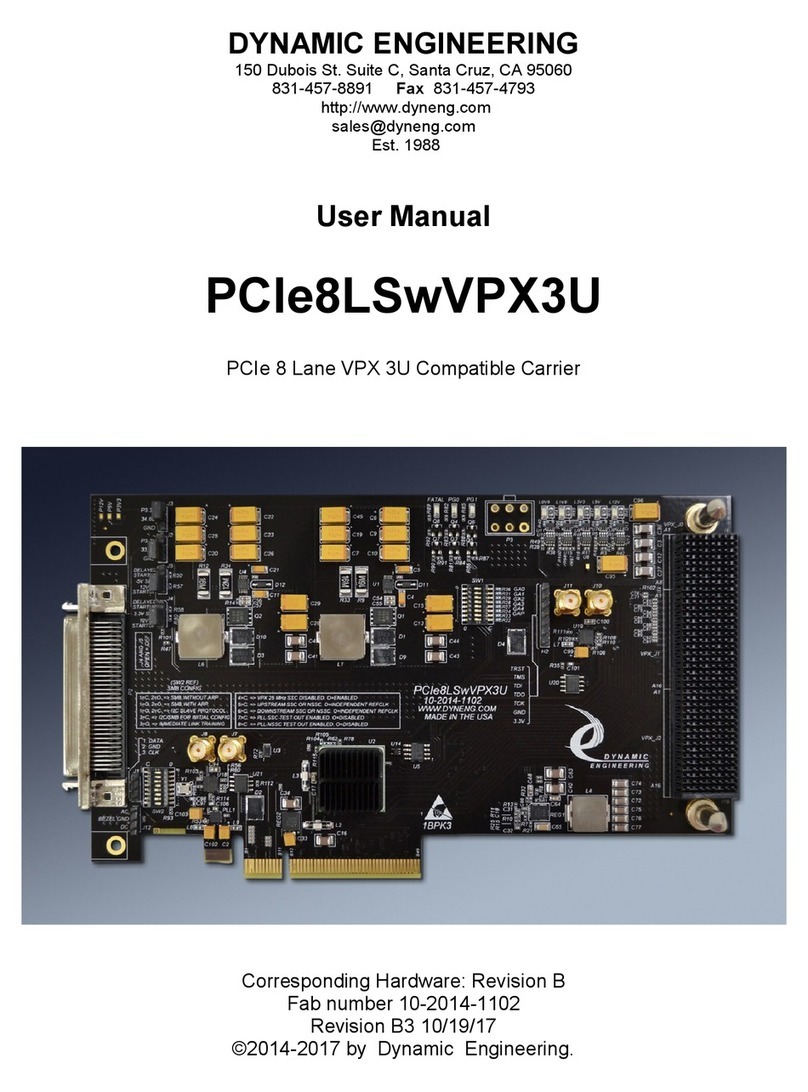
Dynamic Engineering PCIe8LSwVPX3U User manual

Dynamic Engineering
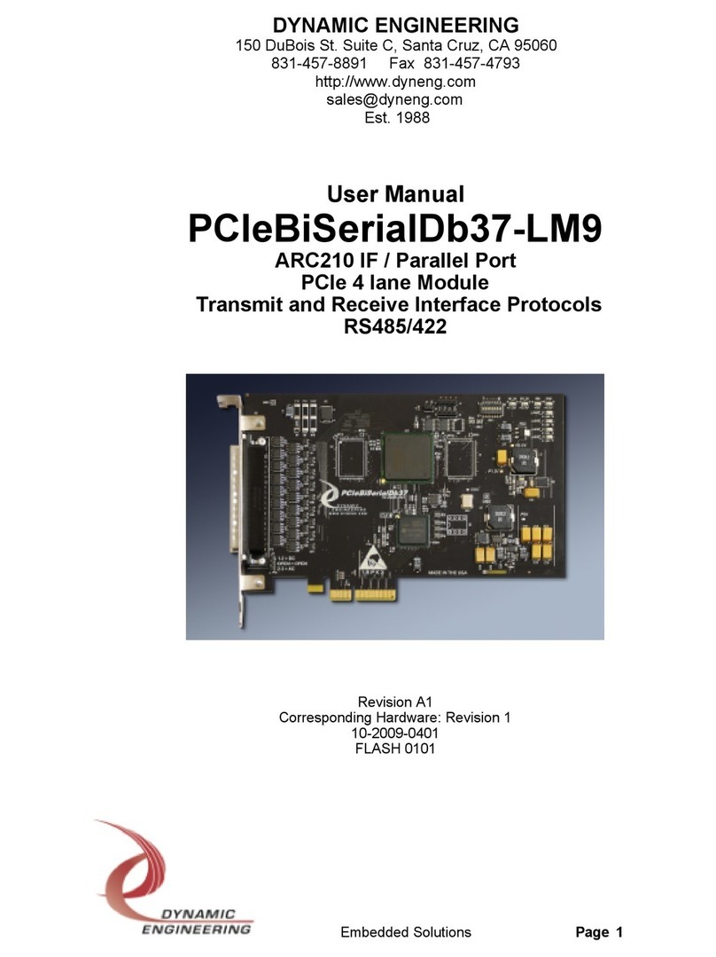
Dynamic Engineering PCIeBiSerialDb37-LM9 User manual

Dynamic Engineering
Dynamic Engineering PCIe8LXMCX2CB User manual

Dynamic Engineering
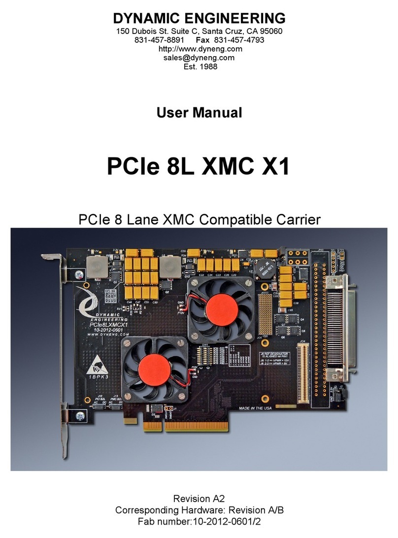
Dynamic Engineering PCIe 8L XMC X1 User manual

Dynamic Engineering
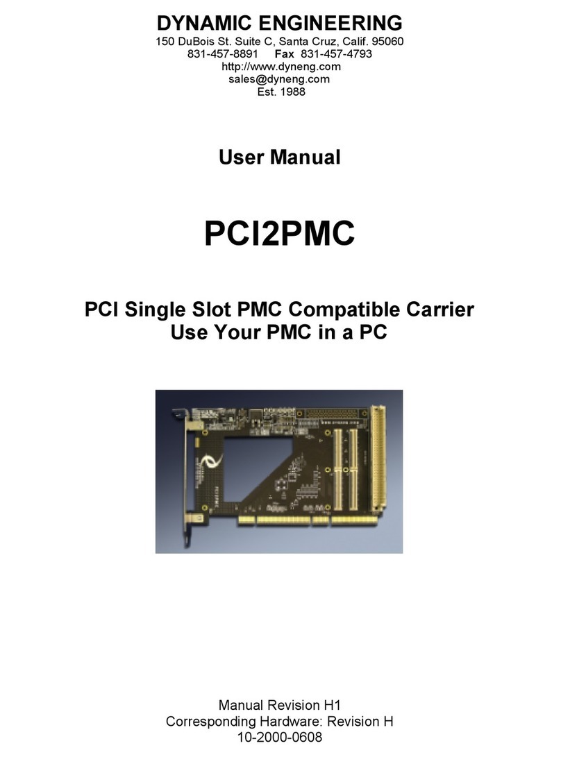
Dynamic Engineering PCI2PMC User manual

Dynamic Engineering
Dynamic Engineering cPCIBPMC6U User manual

Dynamic Engineering
Dynamic Engineering SpaceWire BK User manual

Dynamic Engineering
Dynamic Engineering PC104p-SpaceWire-Monitor User manual