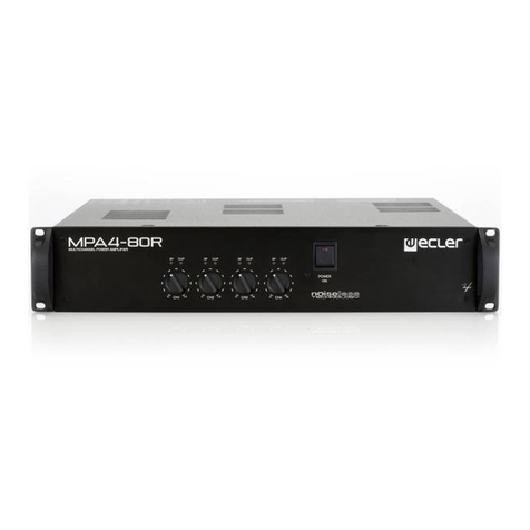
Ecler MPA4-150 User manual

MPA4-150
SERVICE MANUAL
CLIP
4
0
1
2
3
SP CLIP
6
4
CLIPSP
6
0
10
9
8
7
1
2
3
9
7
10
1
82
3
CHANNEL 1
5
CHANNEL 2
5SP
6
4
SP CLIP
6
4
2
010
9
8
7
0
1
3
10
9
8
7
CHANNEL 3
5
CHANNEL 4
5
POWER
4-150AMP
POWER AMPLIFIER
MULTICHANNEL
ON
OFF
CE ELR
VOL VOL VOL VOL TH

SERVICE MANUAL MPA4-150
INDEX
-BLOCK DIAGRAM
-SCHEMATICS
-COMPONENTS LOCATION SCHEMA AND PART LIST
-TESTING AND QUALITY CONTROL
-TECHNICAL CHARACTERISTICS
-WIRING DIAGRAM
-MECHANICAL DIAGRAM
-PACKING DIAGRAM


52-0006-0101 EP05-99 anglès.doc 1 of 2
The amplifying stage basic structure is actually the one commonly used until now, this is, a
push-pull mounted A-B class amplifier, using P-type (IRFP9240) and N-type (IRFP240) mosfets.
The system's controlling core is a NE5534 OpAmp, which is internally compensated in order to
obtain an amplifying gain ratio equal or greater than 3. The amplifier's feedback runs through a
resistor and a capacitor associated to the OpAmp's non-inverting input.
Transistors BF471 and BF472 are common-base configured, becoming actually a current
source structure. They accomplish a dual function: on one hand, they polarise the mosfet's
gate-source junction, keeping them on their conduction knee. On the other hand, they carry out
the OpAmp's output voltage variations, referred to signal ground.
The polarisation current adjustment is fixed by a 2k5 trimming potentiometer connected to the
BF transistors base. This current is added to the current source's output, which passes through
the BF-transistors load resistors. The bias current stability against temperature is fixed through
the BD437 transistors. Their temperature- dependent base-emitter voltage curve is used to alter
adequately the current source's reference voltage. As a consequence, if the temperature rises,
the reference voltage decreases, thus the gate-source voltage also does, and finally the bias
current also decreases.
The Zobel network, formed by a resistor-inductor-capacitor group, and which is located at the
amplifier's output, intends to keep the amplifier's load impedance as constant as possible, no
matter which load is connected to the stage's output, or which signal frequency is to be
amplified, in order to prevent an inverted-phase feedback signal.
In order to avoid a DC offset on the output signal, a diac-triac tandem system is used, which
shorts the output to signal ground when the DC level is enough to get the diac triggered. To
prevent this from happening while carrying audio signal (sine-wave, music), the diac's reference
voltage is taken from a filter formed by resistor 33k2 and capacitor 1µ.
The protection circuitry supervises at any time the power consumed by the MOSFETS. The
circuitry basically consists on two sections: MOSFET's drain current (Id) monitoring and drain-
source voltage (Vds) monitoring.
When Id exceeds a fixed values a control transistor in every branch starts to conduct like a
switch, apliying a parallel resistor to BF's load resisitor, reduring the gate-source voltage, and
also reducing Id.
If the MOSFET's drain-source voltage (Vds) drops too low, a second circuitry actuates to alter
the control-transistor's triggering level, obtaining a SOA-like curve section and a current stage,
which can be adjusted adequately in order to maintain the MOSFET's power consumption as
close as possible to its SOA.
author: J. Colomines date: 050401 project:
EP05-99
product:
MPA4-150
E
C
LER approved:
num: 52.0006 version: 01.01
title:
FUNCTIONING DESCRIPTION

52-0006-0101 EP05-99 anglès.doc 2 of 2
Moreover, the amplifier also includes an ANTICLIP system.
When the amplifier reaches its clipping level, the OpAmp becomes unable to keep the system
under control, and as a consequence ±V peaks appear at its output (15V power supply). This
peaks are used to be rectified and sent to an optocupler (led-resistor) which modifies its
impedance as a function of those peaks' amplitude. The resulting impedance is part of a voltage
divider, together with the amplifier's input impedance. So, as the optocoupler increases its
impedance, the amplifier's input signal level decreases until the system becomes stable.
Also a dual-function temperature control circuitry is provided:
- Temperature-depending control of the cooling fan speed, whose voltage supply is variable
between 7 and 14 Vac.
- Amplifier shutdown when temperature exceeds approximately 90ºC.
The circuitry is formed by LM35D-type IC, which acts like a thermal probe, an amplifier, thermal
probe level comparator and a 7805-type voltage regulator.
The amplifier is responsible for the cooling fan speed control. The comparator triggers a relay,
which cuts off the MOSFETs' bias current by shunting a 22Ωresistance to the BF-type
transistors' load resistors. This way, the output signal of the amplifier is effectively cutted off.
The STAND-BY circuit.
This circuit keeps the safety relay closed for about 10 seconds, thus the MOSFET's bias current
is cutted off during this period, until the whole system reaches again a voltage-stable situation.
Due to this, hearing annoying transients and noises during start up through the loudspeakers is
avoided. This delay is obtained by a RC-cell, where R=287K, and C=47µF/50V. During start up,
this RC-cell's voltage smoothly rises until the 40106-type Trigger-Schmitt trigging level is
reached, and the amplifier starts functioning. C=47µF resets or discharges when the unit is
turned off. During a short period of time, a BC817-type transistor acts like a switch, connecting
two 75Ωparallel resistors to C=47µ/50V.

author: Queralt date: 000719
approved:
num: 52.0006 version: 01.00
FUNCTIONING DESCRIPTION
title:
EP05-99
The amplifying stage basic structure is actually the one commonly used until now, this
is, a push-pull mounted A-B class amplifier, using P-type (IRFP9240) and N-type
(IRFP240) mosfets.
The system's controlling core is a NE5534 OpAmp, which is internally compensated in
order to obtain an amplifying gain ratio equal or greater than 3. The amplifier's
feedback runs through a resistor and a capacitor associated to the OpAmp's non-
inverting input.
Transistors BF871 and BF872 are common-base configured, becoming actually a
current source structure. They accomplish a dual function: on one hand, they polarise
the mosfet's gate-source junction, keeping them on their conduction knee. On the other
hand, they carry out the OpAmp's output voltage variations, referred to signal ground.
The polarisation current adjustment is fixed by a 2k5 trimming potentiometer connected
to the BF transistors base. This current is added to the current source's output, which
passes through the BF-transistors load resistors. The bias current stability against
temperature is fixed through the BD437 transistors. Their temperature- dependent base
emitter voltage curve is used to alter adequately the current source's reference voltage.
As a consequence, if the temperature rises, the reference voltage decreases, thus the
gate-source voltage also does, and finally the bias current also decreases.
The Zobel network, formed by a resistor-inductor-capacitor group, and which is located
at the amplifier's output, intends to keep the amplifier's load impedance as constant as
possible, no matter which load is connected to the stage's output, or which signal
frequency is to be amplified, in order to prevent an inverted-phase feedback signal.
In order to avoid a DC offset on the output signal, a diac-triac tandem system is used,
which shorts the output to signal ground when the DC level is enough to get the diac
triggered. To prevent this from happening while carrying audio signal (sine-wave,
music), the diac's reference voltage is taken from a filter formed by resistor 33k2 and
capacitor 1µ.
The protection circuitry supervises at any time the power consumed by the MOSFETS.
The circuitry basically consists on two sections: MOSFET's drain current (Id) monitoring
and drain-source voltage (Vds) monitoring.
When Id exceeds a fixed values a control transistor in every branch starts to conduct
like a switch, apliying a parallel resistor to BF's load resisitor, reduring the gate-source
voltage, and also reducing Id.
If the MOSFET's drain-source voltage (Vds) drops too low, a second circuitry actuates
to alter the control-transistor's triggering level, obtaining a SOA-like curve section and
a current stage, which can be adjusted adequately in order to maintain the MOSFET's
power consumption as close as possible to its SOA.
ECLER
Sheet 1 of 2
author: Queralt date: 000719
approved:
num: 52.0006 version: 01.00
FUNCTIONING DESCRIPTION
title:
EP05-99
ECLER
Moreover, the amplifier also includes an ANTICLIP system.
When the amplifier reaches its clipping level, the OpAmp becomes unable to keep the
system under control, and as a consequence ±V peaks appear at its output (15V
power supply). This peaks are used to be rectified and sent to an optocupler (led-
resistor) which modifies its impedance as a function of those peaks' amplitude. The
resulting impedance is part of a voltage divider, together with the amplifier's input
impedance. So, as the optocoupler increases its impedance, the amplifier's input signal
level decreases until the system becomes stable.
Also a dual-function temperature control circuitry is provided:
- Temperature-depending control of the cooling fan speed, whose voltage supply is
variable between 7 and 14 Vac.
- Amplifier shutdown when temperature exceeds approximately 90ºC.
The circuitry is formed by LM35D-type IC, which acts like a thermal probe, an
amplifier, thermal probe level comparator and a 7805-type voltage regulator.
The amplifier is responsible for the cooling fan speed control. The comparator triggers a
relay, which cuts off the MOSFETs' bias current by shunting a 22Ωresistance to the
BF-type transistors' load resistors. This way, the output signal of the amplifier is
effectively cutted off.
The STAND-BY circuit.
This circuit keeps the safety relay closed for about 10 seconds, thus the MOSFET's
bias current is cutted off during this period, until the whole system reaches again a
voltage-stable situation. Due to this, hearing annoying transients and noises during start
up through the loudspeakers is avoided. This delay is obtained by a RC-cell, where
R=287K, and C=47µF/50V. During start up, this RC-cell's voltage smoothly rises until
the 40106-type Trigger-Schmitt trigging level is reached, and the amplifier starts
functioning. C=47µF resets or discharges when the unit is turned off. During a short
period of time, a BC817-type transistor acts like a switch, connecting two 75Ωparallel
resistors to C=47µ/50V.
Sheet 2 of 2


Table of contents
Other Ecler Amplifier manuals

Ecler
Ecler DPA600 User manual

Ecler
Ecler VEO-SPH48 User manual

Ecler
Ecler Dante VIDA-24Q User manual

Ecler
Ecler DPA2500T User manual

Ecler
Ecler MPA6-150 User manual

Ecler
Ecler LPA6000 User manual

Ecler
Ecler UMAi SERIES User manual

Ecler
Ecler DPA2500T User manual

Ecler
Ecler eGPA SERIES User manual

Ecler
Ecler eWAMPBT+ User manual

Ecler
Ecler Dante VIDA-24Q User manual

Ecler
Ecler MPA4-150R User manual

Ecler
Ecler MPA4-400 User manual

Ecler
Ecler AMPACK Series User manual

Ecler
Ecler DLA600B User manual

Ecler
Ecler AMBIT SB110 User manual

Ecler
Ecler MPA6-80R User manual

Ecler
Ecler SAM412T User manual

Ecler
Ecler DPA2000 User manual

Ecler
Ecler LP10000 User manual