Icom IC-3200A User manual

144/430MHZ DUAL BAND
FM TRANSCEIVER
c-3aooA/E
SERVICE MANUAL
Downloaded by
RadioAmateur.EU
CD ICOM
ICOM INCORPORATED
1'6-19, Kamikuratsukuri. Hirano-ku. Osaka 547, Japan
Phone: (06) 793-5301
Telex: ICOM TR J63649
ICOM AMERICA, INC.
2380 116th Avenue N.E.
Bellevue, Washington 98004
Phone: (206)454-8155
Telex: 230-152210 ICOM AMER BVUE
FAX :(206)454-1509
3331 Towerwood Drive
Suite 307
Dallas, Texas 75234
Phone:(214)620-2781
Telex: 230-730901 ICOM AMER DAL
1777 Phoenix Parkway
Suite 201
Atlanta, Georgia 30349
Phone: (404)991-6166
ICOM EUROPE G.M.B.H
Himmelgeister Strasse 100
4000 Dusseldorf 1
West Germany
Phone:0211-346047
Telex: 41-8588082 ICOM D
Fax :211-333639
ICOM CANADA LTD.
3071 -#5 Road, Unit 9
Richmond, B.C,
Canada V6X 2T4
Phone: (604)273-7400
Fax :(604)325-0828
ICOM AUSTRALIA, PTY., LTD.
7 Duke Street, Windsor 3181
Victoria, Australia
Phone: (03)529-7582
Telex: 71-35521 ICOMAS

FOREWORD
Thank you for selecting ICOM’s versatile IC-3200A/E, one of the finest FM mobile
transceivers on the market today.
Sophisticated in design, yet light, compact and easy to operate, the 1C-3200A/E
benefits from the latest in ICOM engineering techniques and from ICOM's established
leadership in the communications field.
The pfctufe shows the IC-S300E version.
ASSISTANCE
Three separate versions of the IC-32D0A/E have been designed for use in the
Europe, and Australia. This service manual covers every version. When using the
manual each model can be referred to by the following assigned version numbers:
#03 U,S.A. version
#04 EUROPE version
#05 (VK) AUSTRALIA version
If you require assistance or information regarding the operation and capabilities of the
1C-3200A/E, please contact your nearest authorized ICOM Dealer or ICOM Service
Center,

TABLE OF CONTENTS
SECTION 1SPECIFICATIONS 1—1
1
-1GENERAL 1—1
1-2TRANSMITTER 1—1
1-
3RECEIVER 1—1
SECTION 2OPERATING CONTROLS AND INDICATORS 2—1- 2
2-1FRONT PANEL 2—1
2-
2DISPLAY 2—2
2-3REAR PANEL 2—2
SECTION 3CIRCUIT DESCRIPTION 3—1- 6
3-
1RECEIVER CIRCUITS 3—1
3-2TRANSMITTER CIRCUITS 3—1
3-3 PLL (PHASE-LOCKED LOOP) CIRCUITS 3—3
3-
4LOGIC CIRCUITS 3—4
SECTION 4VOLTAGE/CIRCUIT DIAGRAMS 4-1-9
4-
1WIRING DIAGRAM 4—1
4-2 EF (VOL AND SQL) UNITS 4—2
4-3 MAIN (UHF) UNIT 4—3
4-4 MAIN (VHF) UNIT 4—4
4-5PLL-YGR (UHF) UNIT 4—5
4-6PLL-YGR (VHF) UNIT 4—6
4-7 LOGIC AUNIT 4—7
4-8 LOGICS UNIT 4—8
4-
9PA (UHF, VHF) UNITS 4—9
SECTION 5MAINTENANCE AND ADJUSTMENT 5—1- 7
5-
1PREPARATION BEFORE SERVICING 5—1
5-2 PLL ADJUSTMENT 5—2
5-3 RECEIVER ADJUSTMENT 5—3
5-4TRANSMITTER (UHF BAND) ADJUSTMENT 5—4
5-5TRANSMITTER (VHF BAND) ADJUSTMENT 5—6
SECTION 6TROUBLESHOOTING 6—1- 2
SECTION 7INSIDE VIEWS 7—1- 4
7-1 MAIN UNIT 7—1
7-2PLL-YGR UNIT (IC-3200A/VK VERSIONS) 7—2
7-3PLL-YGR UNIT (IC-3200E VERSION) 7—3
7-
4LOGIC UNITS 7—4
SECTION 8DISASSEMBLY AND ASSEMBLY DIAGRAMS 8—1- 4
8-1FRAME DISASSEMBLY 8—1
8-2FRONT PANEL DISASSEMBLY 8—2
8-
3MAIN UNIT CONNECTOR ASSEMBLY 8—3
8-4 PLL-YGR CONNECTOR ASSEMBLY 8—4

SECTION 9BOARD LAYOUTS 9—1- 6
9-1 MAIN UNIT 9—1
9-2PLL-YGR UNIT 9—2
9-3 LOGIC AUNIT 9—3
9-4 LOGICS UNIT 9—3
9-5 PA (VHP) UNIT 9—4
9-6 PA(UHF)UNIT 9—4
9-7 TX VCO UNIT 9—5
9-8 RX VCO UNIT 9—5
9-9 EF (VOL) UNIT 9—6
9-10 EF (SQL) UNIT 9—6
SECTION 10 BLOCK DIAGRAM 10 —1
SECTION 11 1C RATINGS 11—1-11
SECTION 12 OPTIONAL UNITS 12 —1-2
SECTION 13 PARTS LIST 13 —1-10
EF (VOL AND SQL) UNITS 13—1
MAIN UNIT 13—1
RX VCO UNIT 13 —3
TX VCO UNIT 13 —4
PLL-YGR UNIT 13 —4
LOGIC AUNIT 13 —7
LOGICS UNIT 13 —8
PA (UHF AND VHF) UNITS 13 —9
SECTION 14 SCHEMATIC DIAGRAM SEPARATE

SECTION 1SPECIFICATIONS
1-1 GENERAL
Number oi semiconductors
Frequency coverage and
Channel resolution
Usable temperature range
Frequency control
Frequency stability
Power supply requirement
Current drain (T3.8V DC}
Memory channels
Antenna impedance
Weight
Dimensions
Transistors 49
FETs 10
Diodes 85
VERSION BAND FREQUENCY
COVERAGE
(MHz)
CHANNEL
RESOLUTION
(kHz)
IC-3200A VHF 140.0- 150,0 15 or 5
U.S.A. UHF 440.0-450,0 25 or 5
IC-3200E
EUROPE VHF
UHF 144.0- U6-0
430-0 —440.0 25 or 12.5
IC-3200A
VK VHF
UHF 144.0- 148.0
430.0 -440.0 25 or 5
•10"C +60'^C
(+14-"F~140^ F)
Micro computer-based 5kHz steps (or 12.5kHz steps) Digital PLL
synthesizer with independent dual VFO capability
Within ±0.001%
13,8V DC ±15% (negative ground)
7.5A maximunn
Transmitting
HIGH (25W) :Approx. 7.5A
LOW (5W) :Approx. 3.5A
Receiving
At max. audio output :Approx. 0.65A
Squelched Approx. 0.5A
10 channels with any in-band frequency programmable
SOD unbalanced
1.9kg
140(140)mm(W) x50[50)mm(H) x207(2l3)mm(D)
Bracketed values include projections
1-2TRANSMITTER
Output power
Emission mode
Modulation system
Max. frequency deviation
Spurious emissions
Microphone
Operating modes
HIGH:25W, LOW: 5W
16F3 (F3E 16KO)
Variable reactance frequency modulation
±5kHz
More than 60dB below carrier
600 Delectret condenser microphone with Push-To-Talk and
frequency UP/DOWN SWITCHES
IC-3200A (U.S.A. version only): 16 Key DTMF pad
IC-3200E: 1750Hz Tone Burst unit
Simplex, Semi-duplex, Programmable
1-3RECEIVER
Receiving system
Modulation acceptance
Intermediate frequencies
Selectivity
Sensitivity
Audio output power
Audio output impedance
Double-conversion superheterodyne
16F3 (F3E 16KO)
1st: 30.875MHz
2nd: 455kHz
More than 15kHz at -6dB point
Less than 30kHz at—60dB point
Less than 0.2juV tor l2dB SINAD
Less than 0.4;uV for 20dB noise quieting
More than 1.7W at 10% distortion with 8Q load
4-8D
NOTE: Specifications are approximate and are subject to change without notice or obligation.
Downloaded by
RadioAmateur.EU
1—1

SECTION 2OPERATING CONTROLS AND INDICATORS
2-1 FRONT PANEL
(D © ® ® ®®
IA.fB
I
i
I
1
P^1
IK
||nggH
Fefer to SECTION 2-2. S ®
MR
1«^1
CHECK
MW
>1
m-skip
TS PRIO TONE TCALL 1CALL 2
VFO A
VFO B1888.88s -8 mCALL 2
TONE
®VOLUME AND POWER CONTROL
®SQUELCH AND RF POWER CONTROL
®TUNING CONTROL
©MHz DOWN SWITCH
®MHz UP SWITCH
®A/B AND TUNING SPEED SWITCH
®MEMORY READ AND OFFSET CHECK SWITCH
®MEMORY WRITE AND MEMORY SKIP SWITCH
®SCAN AND SELECTIVE MEMORY SCAN SWITCH
®PRIORITY AND LOCK SWITCH
®CALL 1AND CALL 2SWITCH
®TONE SWITCH AND OFFSET WRITE SWITCH
®OFFSET AND OFFSET WRITE SWITCH
®TRANSMIT AND RECEIVE INDICATORS
®MIC CONNECTOR
®FUNCTION SWITCH
®FUNCTION LED INDICATOR
2—1

2-2DISPLAY
® © ® ®d®
/s f.
PRIO
JVFO Ai
flVFO BI
DUP+DUP-
CALL 1CALL 2
S/RF 1
@
®FREQUENCY DfSPLAY
(?) FUNCTION INDICATOR
©VFO INDICATORS
©MEMORY CHANNEL INDICATOR
®PRIO INDICATOR
©TS INDICATOR
@TONE INDICATOR
®CALL 1INDICATOR
®CALL 2INDICATOR
®DUPLEX INDICATORS (+/-)
®S/RF LEVEL METER
2-3REAR PANEL
®EXTERNAL SPEAKER JACK
(i) POWER' CONNECTOR
®ANTENNA CONNECTOR^
©POWER CONNECTOR
®ANTENNA CONNECTOR
@EXTERNAL SPEAKER JACK
2—2

SECTION 3CIRCUIT DESCRIPTION
3-1RECEIVER CIRCUITS
3-1-1 VHF ANTENNA SWITCHING CIRCUIT
(PA UNIT)
Incoming VHF signals from the antenna connector are
passed through aChebyshev Low-pass filter consisting of
L3, L4, L6, Cl 2, Cl 3, Cl 4, and Cl 5, and are fed to the
antenna switching circuit. While receiving, D2 is turned ON.
Receive signals from alow-pass filter are passed through
another filter consisting of Cl 0, L2 and Cl 7, and are fed to J1
on the MAIN UNIT.
3-1-2 VHF RF AMPLIFIER CIRCUIT (MAIN UNIT)
Signals from J1 are passed through the L1-L2 bandpass
filter, and are amplified by Q1. Amplified signals from Q1 are
passed through the L3-L4-L5 bandpass filter, and are mixed
with the local oscillator signal from the PLL circuit in Q2 to
produce afirst IF signal of 30.875MHz.
3-1-3 UHF ANTENNA SWITCHING CIRCUIT
(PA UNIT)
Incoming VHF signals from the antenna connector are
passed through both aChebyshev low-pass filter consisting
of LI 3, LI 4, C35, C36 and C37 and aChebyshev low-pass
filter consisting of L11, L13, C32, C33 and C34 before being
fed into the antenna switching circuit. While receiving, D5 is
turned OFF. Receive signals from the low-pass filter are
passed through another filter consisting of L10, C30, C39
and C40, and are fed to J3 on the MAIN UNIT.
3-1-4 UHF RF AMPLIFIER CIRCUIT (MAIN UNIT)
Signals from J3 are passed through atuned circuit
consisting of L1 1,C21 and C22, and the output is amplified
by Q5. The output from Q5 is passed through bandpass filter
L13, amplifier Q6, bandpass filter LI 5, and is mixed with the
local oscillator signal from the PLL UNIT to produce afirst IF
signal of 30.875MHz.
3-1-5 IF AMPLIFIER CIRCUIT (MAIN UNIT)
The first IF signal from the mixer is passed through the
L8-C1 2tuned circuit, is filtered by crystal filter Fit ,is passed
through the L9-C15 tuned circuit, and is amplified by Q4. D3
and D4 function as alimiter for strong signals. The amplified
signal from Q4 is fed to pin 16 of IC1. IC1 incorporates a
second oscillator, asecond mixer, alimiter and a
discriminator on asingle chip. The signal from pin 16 of IC1
is mixed with the second oscillator signal to produce the
455kHz signal at pin 3on IC1 .The 455kHz signal is filtered by
ceramic filter FI2 and is fed to pin 5of IC1 where it then
enters the limiter amplifier. The amplified signal is fed to the
discriminator through ceramic discriminator unit XI. The
audio signal exits from pin 9on IC1.
3-1-6 AUDIO AMPLIFIER CIRCUIT (MAIN UNIT)
The audio signal from pin 9on IC1 is amplified by Q10, is
filtered by active filter Q11, and is fed through J7 and the
VOLUME CONTROL to pin 1on 105. IC5 is the audio power
amplifier. The amplified audio signal from IC5 is fed to the
speaker through J10.
3-1-7 SQUELCH CIRCUIT (MAIN UNIT)
The audio signal from pin 9on IC1 is also fed to the noise
amplifier through C69, R50, J8, C70, and the SQUELCH
CONTROL and then is input to pin 10on IC1 .The amplified
noise signal exits from pin 11on IC1 ,is rectified by D1 1and
D12, and is controlled by 09 through R54.
3-1-8 S-METER CIRCUIT (MAIN UNIT)
S-meter signals from pin 5on IC1 are amplified by IC3
through C66 and R49, are passed through L20, are rectified
by D9 and DIO, and are fed to the LCD driver circuit on the
LOGIC AUNIT through J12. In the VHF mode, the band
signal turns ON Q12 to adjust the gain of IC3 by means of
R82, equalizing the S-meter level between VHF and UHF.
3-2TRANSMITTER CIRCUITS
3-2-1 MIC AMPLIFIER CIRCUIT (PLL UNIT)
The microphone output is fed into IC5A through C60andthe
08 amplifier. IC5A includes adifferential amplifier and a
limiter amplifier with R2 as the UHF deviation gain
adjustment and R3 as the VHF deviation gain adjustment.
Preemphasis of 6dB/octave is introduced between 300Hz
and 3kHz. The signal is then fed to the FM modulator in the
TX VCO UNIT through alow-pass filter consisting of IC5B,
R45, R46, R49, C51, C52, and C53.
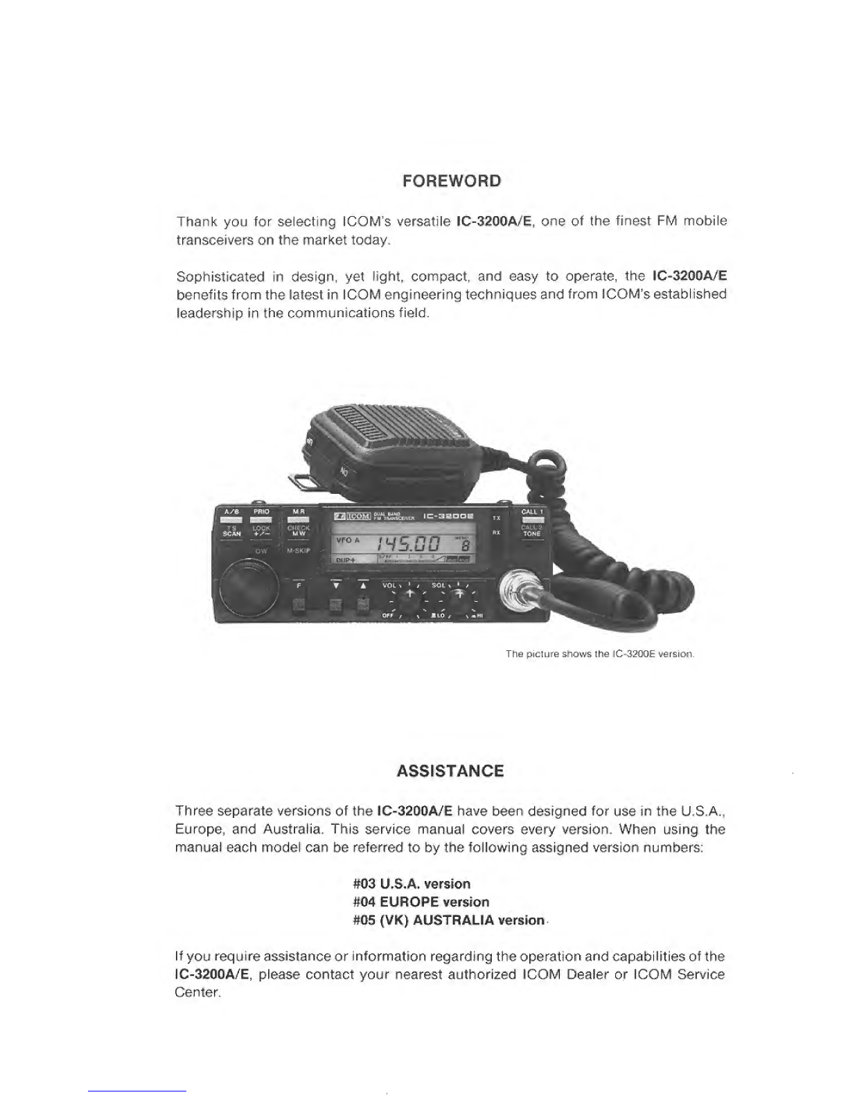
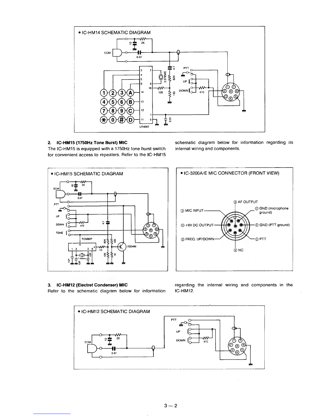
3-2-2 MICROPHONES USED WITH THE IC-3200A/E
The IC-3200A/Ecomesfactoryequipped with a high-quality
electret condenser microphone. The type of supplied
microphone varies with each transceiver model. The
microphone types are listed below.
IC-3200A (#03) ;IC-HM14 (DTMF Encoder)
IC-3200E (#04) ;IC-HM15 (1750Hz Tone Burst)
IC-3200A (#05) :IC-HM12
1. IC-HM14 (DTMF Encoder) MIC
Plug the IC-HM14 into the MIC CONNECTOR on the front
panel for immediate transceiver operation. If you wish to use
adifferent microphone with the IC-3200A, be sure it has the
proper output level before making any connections.
Particular care should be exercised when wiring adifferent
microphone since the internal electrical switching system in
the transceiver depends on proper connections being made.
See the diagram on page 3-2 for proper MIC wiring
instructions.
3— 1

2. IC-HM15 (1750Hz Tone Burst) MIC schematic diagram below for information regarding its
The IC-HM15 is equipped with a1750Hz tone burst switch internal wiring and components,
for convenient access to repeaters. Refer to the IC-HM15
•IC-HM15 SCHEMATIC DIAGRAM •IC-3200A/E MIC CONNECTOR (FRONT VIEW)
ecm|
0.47
PTT o
UP iSz: r
<~v.
DOWN 1L7 ^rVV
1Q1470
TONE 1°
1oTC5082P
5
12 39
llnDl-4a
'riXs XX
©MIC INPUT-
®+8V DC OUTPUT
@FREQ, UP/DOWN
®AF OUTPUT
(D
®GND (microphone
ground)
®GND (PTT ground)
®PTT
3. IC-HM12 (Electret Condenser) MIC
Refer to the schematic diagram below for information
regarding the internal wiring and components in the
IC-HM12.

3-2-3 MULTIPLIER AND DRIVER CIRCUITS
1. VHP Circuit
The RF signal from the PLL UNIT is amplified by IC1 on the
VHF PA UNIT to obtain 25W, and the output from pin 4on
IC1 is fed to the ANT switching circuit. In the transmit mode
D2 and D4 in the T/R switching circuit are turned ON, and L2
and C2 become aparallel resonant circuit. The output power
from pin 4on IC1 is fed to the antenna terminal through the
bandpass filter.
2. UHF Circuit
The RF signal from the PLL UNIT is amplified by IC2 on the
UHF PA UNIT to obtain 25W, and the output from pin 5on
IC2 is fed to the ANT switching circuit. In the transmit mode,
D5 and D7 in the T/R switching circuit are turned ON, and
LI 5and C41 become aparallel resonant circuit. The output
power from pin 5on IC2 is fed to the antenna terminal
through the bandpass filter.
3. VHF/UHF ALC (Automatic Levei Control) Circuit
(PA UNiTS AND MAIN UNIT)
This circuit stabilizes the output power even when the power
supply voltage or the antenna impedance is fluctuating. The
varying current from the power amplifier at R1 (VHF) and R6
and R1 1(UHF) is amplified by the IC2B (VHF) or IC2A (UHF)
differential amplifiers on the MAIN UNIT. The output voltage
is fed to 01 (VHF) or 03 (UHF) which control the current to
the module’s driver stage, maintaining constant RF power.
4. VHF/UHF RF Meter Circuit
(PA UNITS AND MAIN UNIT)
Asample of the RF output power is fed to D3 (VHF) or D6
(UHF) through 09 (VHF) or 027 (UHF), is rectified, and is
passed to the module’s driver stage to maintain constant RF
power.
5. Power Supply Circuit (MAIN UNIT)
The 13.8V from the DC connector is applied to 104 on the
MAIN UNIT through filters consisting of L22, 097, and R89.
This causes 9V to be fed to the MAIN and PLL-YGR UNITS.
3-3 PLL (PHASE-LOCKED LOOP)
CIRCUITS
3-3-1 PLL
The PLL is designed so that the desired frequency is
generated directly by the VCO using adual modulation
prescaler system, and is composed of the IC2 prescaler IC
and the IC1 PLL 10. The PLL circuit is fed “divided-by-N”
DATA from the CPU to determine the operating frequency.
N-DATA is the ratio of the desired frequency (the transmit
frequency in transmit mode and the first local oscillator
frequency in receive mode) and the reference frequency.
_Desired frequency
Reference frequency
Crystal XI oscillates in Q1 and its output signal is divided by
adividing circuit in 101 that obtains areference frequency of
5kHz for the IC-3200A (6.25kHz for the IC-3200E version).
The signal from the VCO that is buffer-amplified at Q6 is
divided Ntimes at 102 and 101 .The signal inside 101 is phase
detected and the detected signal is output from pin 11on
101. The output signal is applied to the TX D1 and TX D2
varactor diodes (or RX D1 and RX D2) in the VCO and is
passed through the Q2-Q3 loop filter to control the VCO
frequency.
3-3-2 VCO/FM MODULATION CIRCUITS
The VCO is composed of the following circuits: VHF RX,
UHF RX, VHF TX, and UHF TX. APD signal from the PLL is
fed to the varactor diode connected to each drain of the
FETs to control the VCO frequency.
1. Dual Modulus Prescaler
102 is adual modulus prescaler that divides the signal
generated by the VCO by either 64 or 65. The VHF receive
range is 102.125~119.125MHz and the transmit range is
140.00—
150.00MHz. The UHF receive range is
409.
125—
419. 125MHz and the transmit range is
440.00—
450.00MHz. 101 is aCMOS LSI chip designed for
use asafrequency synthesizer. It incorporates a6-bit
swallow counter, an 11 -bit programmable counter, aphase
comparator, acharge pump, and afrequency divider for the
reference frequency. The reference frequency from Q1 is fed
to pin 15 on 101. Here the frequency is divided by 1024, the
reference frequency becomes 5kHz (6.25kHz for the
IC-3200E version), and the frequency is fed to pin 2on 101
.
2. VHF/UHF RX VCO Circuit
The RX VCO is aClapp oscillator circuit which oscillates in
the VHF range 107.125—119.125MHz or in the UHF range
409.125—
419.125MHz. The frequency is controlled by the
DC voltage from VRXC on 103. The drains of 01 (VHF) and
Q4 (UHF) receive apositive 9V while the tranceiver is in the
receive mode and 02 (VHF) or 04 (UHF) are turned ON.
Thus the frequency is generated when the FET source is at
ground level.
3. VHF/UHF TX VCO Circuit
The TX VCO is aClapp oscillator circuit. The frequency is
controlled by the DC voltage from V-VCO-C or U-VCO-C
from IC3. When the drains of 06 (VHF) or 03 (UHF) receives
positive 9V, 04 (VHF) or 03 (UHF) turns ON. The VHF
oscillator frequency (140—150MHz) is fed out through C17
and the UHF oscillator frequency (440—450MHz) is fed out
through the 02 multiplier amplifier.
4. Low-pass Filter Circuit
The local oscillator signal from the RX VCO (VHF:
102.125—
119.125, UHF: 409.125MHz) is divided by 2by the
02 multiplier amplifier. The VHF local oscillator signal is fed
to J2 on the MAIN UNIT through D13 and alow-pass filter
consisting of L12, L13, C99, C100 and C101. The UHF local
oscillator signal is fed to J4 on the MAIN UNIT through D12
and alow-pass filter consisting of L10, L11, C94, C95, and
C96.
Downloaded by
RadioAmateur.EU
3—3

5. Tone Circuit
IC-32D0A Version:
TheCTCSStorectrcuit is composed of iC7 and IC8. When a
tone number is selected, data is sent to IC7 from the CPU.
IC7 carries out aeriai/parallei conversion on the data from
the CPU and the results are fed to tCS, IC8 divides the X2
frequency (3,579545MHz) by an amount related to the data
from the CPU^ and the output is fed from pi n1.The CTCSS
tone output level is controfled by R42, then the signal is fed
to the TX VCO UNIT.
IC-3200E Version:
The 1750Hz tone-burst circuit iscomposed of 3CS, Q23, and
Q24. ICS is preset for 1750Hz and outputs the tone signal
from pin 1. When the [TONE] SWITCH on either the
microphone or front panel of the IC-3200E Is pushed, ICS
generates atone and 024 simultaneously makes aSEND
line to ground level, putting thetransceiver in transmit mode.
The 17S0Hz tone output Jevel is conIrolSed by R42 and the
signal Is then fed to the TX VCO UNIT.
TONE FREQUENCY
NO. (Hz)
167.0
271 9
374.4
477.0
579,7
682.5
785,4
S8S.5
991.5
10 94,8
11 97.4
12 100.0
13 103.5
14 107.2
TONE 1FREQUENCY
NO. (Hz)
15 110.9
16 114.8
17 118.8
18 123,0
19 127,3
i20 131.8
21
1136.5
22 141.3
23 146.2
24 151.4
25 156.7
_...
26 1622
27 167.9
28 173.8
TONE
NO. FREQUENCY
(Hz)
29 179,9
30 106.2
31 192,8
32 203,5
33 210.7
34 218.1
35 225.1
36 233,6
37 241.8
38 250.3
6. Voltage Regulator CircutI
{PLL-YGR UNIT)
The supply voltage for the PLL-YGR UNIT includes 10
different values: 13.3V, common 9V, 6V, VR8V, UR8V, VT8V,
UT8V, +8V, UT13.8V, and J8V. These voltages are supplied
to each unit. Acommon 9V from IC4 on the MAIN UNIT is
supplied to the PLL-YGR UNIT. This 9V is connected to the
emitters of Q14 (VT8V), Q13 (UT8V). QIO (VRSV), and Q9
(VRBV). 13.8V isconnected to theemittersofQII (VT13.8V)
and 012 (VT13.SV). Q9, QIO, Oil, Q12, Q13, and Q14 are
PNP transistors which turn ON when their bases are
grounded. The voltage is fed out from the collectors of each
transistor. The bases of 09^ 014 are controlled by lC4and
IC3. IC4 has seven inverter transistors so that when aHIGH
level is applied to IC4 from IC3, the output voltage is LOW.
IC3 is composed of two decoders and ademultipiexer,
IC3 produces a4-bit binary output with two inputs (A and B).
This input is controlled by three signals; SEND (RX: HIGH,
TX: LOW), TX (RX; LOW, TX: HIGH) and BAND A/B (VHP;
LOW. UHF; HIGH), When the PLL is out of lock, the ENABLE
TERMINAL of ICS is HIGH, and all output terminals are
LOW.
3-4 LOGIC CIRCUITS
3-4-1 CPU
The CPU on the LOGIC BUNIT is a4-bit CMOS CPU with an
LCD driver. The initialization matrix on the LOGIC BUNIT
selects the version of the transceiver, and the main matrix on
the LOGIC Aand LOGIC BUNITS controls the functions of
the transceiver.
The CPU controls the PLL, CTCSS and speech synthesizer
ci rcuit by means of serial data through IC4 Dand IG4E on the
LOGIC BUNIT.
1. Memory Backup for CPU
Alithium battery (BT1 on the LOGIC BUNIT) isfor memory
backup when the transceiver is turned OFF. The memory
backup mode begins when apulse is applied to the INTO
port on the CPU, stopping the CPU and saving memory data.
3-4-2 LOGIC AUNIT
1. Stop Circuit
The stop circuit consists of tC3B, iC4B, IC5B, Q7. Q6, arid
DIO. IC3B, Q7, and Q8 function as aNOR gate. D5 and R29
function as an OR gate. IC5B is aSchmitt trigger ci rcuit that
uses the junction voltage of D1 as areference voltage.
Therefore, if the 5V line on the LOGIC AUNIT is more than
4V, IC5B feeds Out aHIGH level and the one shot circuit
consisting of IC4C, C5, and R28 feeds apulse to the INTO
port on the CPU to cancel the CPU mode.
The cathode of Dll is connected to the LCD mute port on
the CPU. When the CPU is in the stop mode, the mute port is
HIGH but when the stop mode is cancelled, the mute port is
LOW. Also, the output levef from the IC3, Q7, and Q3 NOR
gate is LOW. ICABisabufferampiifier which drivesQZ. if the
supplied voltage to 1C5 on the LOGIC AUNIT drops below
3.8V, the output level from 105 will be LOW and the output
level from IC3B will be HIGH. Therefore, the CPU will
activate the stop mode. When the CPU is in the stop mode,
the LCD mute port on the CPU is HIGH, and the outputfrom
JC3B is LOW,
3—4

2.
TX/RX Switching Circuit
When the PTT SWITCH on the microphone is pushed, pin 5
of J1 becomes LOW and thecolfectorof Q4 becomes HIGH.
Q3 reverses this signal to supply the transmit mode signal to
the SEND port on the CPU.
3. TX Control
Pin 13on IC3A is connected to the MUTE port on the CPU to
eliminate unwanted signals from being transmitted. If an
out-of-barid frequency is selected, the output level from
ICSAStays LOW to mute the transmit signal when the PTT
SWITCH on the microphone is pressed.
4. Power ON Reset Circuit
When the transceiver is turned ON, asignal from IC4C is
Supplied to IC3C and the main matrix on the LOGIC AUNIT.
If the FUNCTION SWITCH is pressed when the transceiver
is being switched ON, IC3 sends areset signal to the CPU.
5. Scan Stop Circuit
When the SQL Ssignal from the MAIN UNIT is HIGH, it turns
ONOBand passes thesignal to the SCAN STOP port on the
CPU. Also, 06 controls the D13 receive LED.
a. Mic UP/DOWN Circuit
When the UP/DOWN SWITCH on the microphone is
pressed, asignal is supplied to the MIC CK port on the GPU.
When the UP SWITCH is pushed, the collector of ICS
becomes HIGH. When the DOWN SWITCH is pushed, the
collectorof IC5 becomes LOW. The CPU receives this signal
from the U/D port on the CPU to control the microphone
scanning function
3-4-3 LOGIC BUNIT
1. Initial Matrix CircuUs
IC1, the BCD-To-Decimal Decoder on the LOGIC BUNIT,
decodes the initial matrix signal generated by the following
diodes on each lC-3200 version:
(4) Q5 -A1 (Ax)
This matrix sets the frequency step and the reference
frequency of the PLL circuit on BAND B. When the
matrix (especially Q5 —At) is ON, areference
frequency of 6.25kHz is selected; when Q5 At is OFF, a
reference frequency of 5kHz is selected.
Q5 Ax (REFERENCE 3}
This matrix sets the frequency step on BAND B.
(5) Q6->^A2(OWA)
This matrix setstheoffset frequency in duplex mode on
BAND Awhen transceiver power is turned ON. When
the matrix Q6 A1 is ON, ani offset frequency of 600kHz is
selected.
(6) Q7 -A1(A4KOWB)
This matrix sets the offset frequency in duplex mode on
BAND Bwhen transceiver power is turned ON. When
the matrix Q7 A4 is ON, an offset frequency of 5.0MHz is
selected. When both Q7 A1 and Q7 A4 are ON, an offset
frequency of 7.6MHz is selected for the IC-3200E
version.
(7) 09 A1 (VOICE SYNTHESIZER ON/OFF}
This matrix setsthe ON or OFF condition forthe signals
of the voice synthesizerunit, When the matrix is OFF. no
data signals for the voice synthesizer are output. When
the matrix is ON, the data signals are output.
r~
1
1
All-
15£1U
J
yis&i;iii
^001 J
y1
-
1
IC-3200A A?!—
kSSi.53j
’y *iSS>3J,
1
1
A' 1
iSSiM, 15.5133.
Thi* ^
A.15513a
y.ISElLtJj yh
[
Aq 1
AaJ' s
—
L. .J
Qfl. 07 Ofi 0& Q.'. Q3 02 01 QO
(1) Qo Ax (BAND A/VHF}
This matrix sets the frequency bandwidth on the VHF
(BAND AJ.
NOTE: The value of xwill vary with each transceiver
version.
{2}01 Ax (BAND B/UHF)
This matrix sets the frequency bandwidth on the UHF
(BAND B).
IC-3200A
(VK)
(3) Q4 -A1 (AX> (REFERENCE A)
This matrix sets the frequency step and reference
frequency of the PLL circuit on BAND A. When the
matrix fespecialiy 04 —A1) is ON, areference
frequency of 6.25kHz is selected; when Q4 —A1 is
OFF, areference frequency of 5kHz is selected. IC-3200E
Q4 -Ax
This matrix sets the frequency step on BAND A,
I
riS5'33
yj
/iSSiM
y1
^(
1
iSilSjj
yhIS512J.
y¥1
1
1—a5Sii3,
yISS133 *1
1
1
1—
'
1
1
1
hy1jAS 1U,
y*
1
1
1
I. .J
07 06 05 Qi 03 Q? 01 0<5
3—5

2. Matrix Switch
The matrix data from the LOGIC B UNIT are fed to B1, B2,
and B4 on the CPU through SI to activate the scan speed,
the scan timer, and the memory lock functions.
3. Busy Matrix for the Speech Synthesizer
When the speech synthesizer is activated, it sends abusy
signal to D3, and turns ON D1 B2 on the main matrix by
means of 01 .This alerts the CPU that the synthesizer is
activated. The CPU waits until the busy signal is LOW before
continuing.
4. BEEP Circuit
The BEEP circuit is aphase oscillator consisting of IC3D, R5,
R6, R7, C9, Cl 0, and Cl 1which feeds out a signal to 01 3on
the MAIN UNIT when the control gate is HIGH.
5. DIAL Clock Circuit
This circuit consists of IC2, IC3, 02, R9, RIO, R11, C6 and
C7, which form the rotary encoder. When turning the
encoder dial, one shot pulses are generated from IC2A.
Meanwhile, 02 generates aHIGH or LOW signal to the U/D
port on the CPU for UP or DOWN tuning. Also, IC2A sends
sensor signals to the CK port on the CPU.
3—6


t-3MAIN (UHF) UNIT
ROV
iCI
12—46711
6.2V I.OV 0.9V IWPl 2.0V
l|Q[ mm 0V 0 V0V
DC Voltage by 50kD/V multimeter
14 mm
0V0V2.0V
I2
0V
0V


4-4MAIN (VHF) UNIT
to PA(VHF)P6
to PLL P2
to PLL J4
9V
UR8
Vl^
BANDAB
VT8
UT8
13.8(2)
E
toPA(UHF)P8
to PLL PI
to PA(UHF)P3
APC
E
PAV
HV
RFM
UT8V
toPA(VHF)PI
APC
E
PAV
HV
RFM
VT8V
to LOGIC BP3
9V
E
AFB
SOLS
S/RFM


4-5PLL-YGR (UHF) UNIT lO
CL
O
ODownloaded by
RadioAmateur.EU
Other manuals for IC-3200A
2
This manual suits for next models
1
Table of contents
Other Icom Transceiver manuals