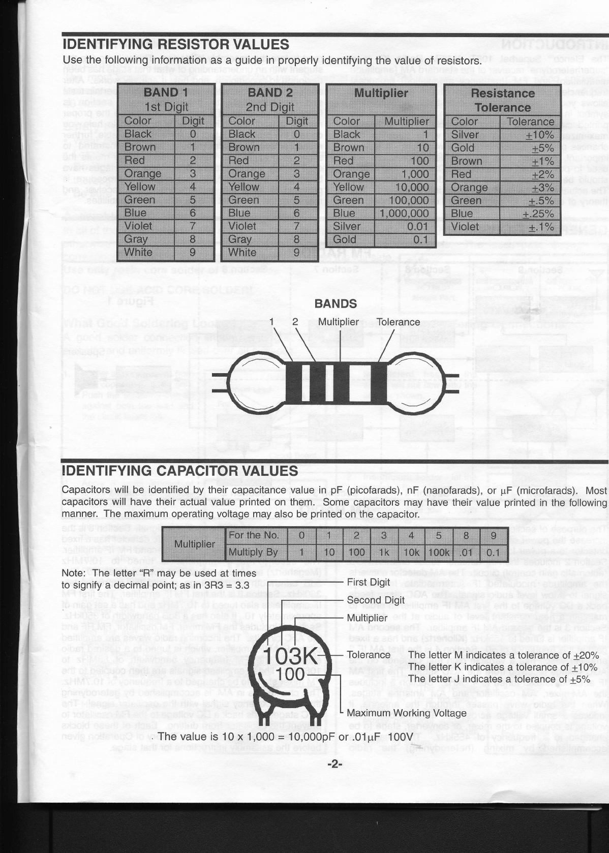
Elenco Electronics AM/FM-108TK User manual

MODEL AM/FM.I OSTK
14 TRANSISTORS, 5 DIODES
llillll|Itililffiil
Assembly and lnstruction Manual
Elenco'" Electronics, lnc.
Copyright @2004,2000 by Elenco'" Electronics, lnc. All rights reserved. Revised 2004 REV-H 7535087
No part of this book shall be reproduced by any means; electronic, photocopying, or otherwise without written permission from the publisher.

The AM/FM Radio project is divided into two parts, the AM Radio Section and the FM Radio Section. At this time, or
identify the parts that you will need for the AM radio as listed below. DO NOT OPEN the bags listed for the FM radio.
."p"r"t" parts list will be shown for the FM radio after you have completed the AM radio.
ffiTHE AM RADIO SECTION
lf you are a student, and any parts are missing or damaged, please see instructor or bookstore. lf you purchased this
from a distributor, catalog, eic., please contact Elenco" Eiectronics (addressiphone/e-mail is at the back of this manual) 1
additional assistance, if ieeded. DO NOT contact your place of purchase as they will not be able to help you.
Qty.
n1
Z4
n1
n1
tr1
!1
n3
n1
tr1
n1
n1
n1
!1
n1
n1
Symbol
R46
R38,43, 48,49
R47
R41
R37
R42
R33, 36, 44
R40
R32
R35
R39
R31
R45
R34
Volume/S2
Value
47A5"/" 1l4W
100o 5% 1/4W
330f) 5% 1/4W
470A5% 1l4W
1ka5% 1l4W
2.2kf)5% 1l4w
3.3kO 5% 1l4w
1oko 5% 1/4W
12kO5% 1l4W
27kA 5Y" 1l4W
39kO 5% 1/4W
56kO 5% 1/4W
470ko5% 1l4w
1MO 5% 1/4W
sOKO / SW
Color Code
Vellow-violet-black-gold
brown-black-brown-gold
orange-orange-brown-gold
vel low-violet-brown -gold
brown-black-red-gold
red-red-red-gold
orange-orange-red-gold
b rowh-black-oran ge- gold
brown-red-orange-gold
red-violet-orange- gold
orange-white-o ran ge-gold
qreen-blue-orange-gold
yellow-violet-yellow-gold
brown-black-green-gold
PoVSW with nut and washer
Part i
12470
13100
1 3330
13470
14100
14220
1 4330
15100
15124
1527C
1 539C
1 556C
1647C
1710C
19252
Qty. Symbol
tr1 c30
n1 C44
a2 c31, 38
n5 c29, 33, 35, 36, 37
n1 c28
tr3 C32,40,41
!1 C42
n1 C34
J2 c39,43
!1 c1
Value
150pF
.001pF
.01uF
.O2iiF or .O22pF
.1pF
1 OpF
47p,F
1 00pF
47Op,F
Variable
PACITORS
Description
Discap (151)
Discap (102)
Discap (103)
Discap (203) or (223)
Discap (104)
Electrolytic Radial (LYtic)
Electrolytic Radial (Lytic)
Tuning Gang AM/FM
Part
22151
231 0t
2410i
24201
251 01
2710t
2747t
2810t
2847t
2999(
SEMICONDUCTORS
Qtv.
a2
n5
n1
n1
n1
Symbol
D4,5
Q7, 8, 9, 10, 11
Q12
Q14
Q13
Value
1 N4148
2N3904
2N3906
MPS6560 or 8050
MPS6562 or 8550
Description
Diode
Transistor NPN
Transistor PNP
Transistor NPN
Transistor PNP
Part
3141,
3239(
3239(
3280i
32851
Qty. Symbol
n1 L5
!1 T6
n1 T7
n1 T8
!1 L4
COILS
Color DescriPtion
Red AM Oscillator
Yellow AM lF
White AM lF
Black AM lF
AM Antenna with Holders
Part #
430057
430260
430262
430264
484004
MISCELLANEOUS
MAGIC WAND
Qty. DescriPtion
n 1 lron Core
tr 1 Brass Core
a4" Shrink Tubing
Part
461 01
661 1
8901
Pat
6411
641|
6441
645
6651
723.
780
81 41
o(
Qtv.
u1
!1
tr1
n1
!1
n1
n1
n1
n1
Description
PC Board
Switch
Battery Holder
Speaker
Knob (pot)
Knob (dial)
Earphone Jack with Nut
Radio Stand
Earphone
Part #
517054
541023
590096
5901 02
622017
622030
622130 or 622131
6261 00
629250
Qtv.
n3
n3
n3
n1
!8
tr1
n1
n6"
n1
Description
Screw 2-56 x 114"
Screw M2.5
Nut 2-56
Plastic Washer
Test Point Pin
LabelAM/FM
Speaker Pad
Wire 22 insulated
Solder
---- SAVE irre EOX THAT THIS KIT CAME IN. IT WILL BE USED ON PAGES 24 & 53. ****

IDENTIFYING RESISTOR VALUES
Use the following information as a guide in properly identifying the value of resistors.
BANDS
2 Multiplier Tolerance
IDENTIFYING CAPACITOR VALU ES
Capacitors will be identified by their capacitance value in pF (picofarads), nF (nanofarads), or pF (microfarads). Most
capacitors will have their actual value printed on them. Some capacitors may have their value printed in the following
manner. The maximum operating voltage may also be printed on the capacitor.
Note: The letter "R" may be used at times
to signify a decimal point; as in 3R3 = 3.3 First Digit
Second Digit
Multiplier
Tolerance The letter M indicates a tolerance ol +20"k
The letter K indicates a tolerance ol +10.k
The letter J indicates a tolerance ol +5./"
Maximum Working Voltage
The value is 10 x 1 ,000 = 10,000pF or .01 pF 100V
1 03K
r 100
\-.l
-2-

INTRODUCTION
The Elenco" Superhet 108T AM/FM Radio Kit is a
"superheterodyne'; receiver of the standard AM (amplitude
mobulation) and FM (frequency modulation) broadcast
frequencies. The unique design of the Superhet 108
allows you to place the parts over their corresponding
symbol in the schematic drawing on the_surface of the
printeO circuit board during assembly' This technique
maximizes the learning process while keeping the
chances of an assembly error at a minimum. lt is very
important, however, that good soldering practices are
used to prevent bad connections' The Soldering Guide
should be reviewed before any soldering is attempted.
The actual assembly is broken down into 9 sections. The
theory of operation'for each section, or stage, should be
read before the assembly is started' This will provide
student with an understanding of what that stage has bt
designed to accomplish, and how it actually works' A
each assembly, you will be instructed to make certain te
and measurements to prove that each section
functioning properly. lf a test fails to produce the pro
results, a-troubleshooting guide is provided to help '
correct the problem. lf test equipment is available, furt
measurements and calculations are demonstrated
allow each student to verify that each stage meets
engineering specifications. After all ol the stages h
been built and tested, a linal alignment procedure
provided to peak the performance of the receiver i
maximize the Superhet 108T's reception capabilities.
GENERAL DISCUSSION
Section 9Section 8FM RADIO
Section 7Section 6
I
I
t
-----J
I
I
I
-----J- I
I
I
I
-l-
Section 5Section 4Section 2
Figure 1
Section 1
Section 3
AM RADIO
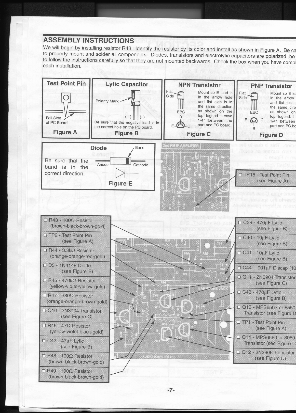
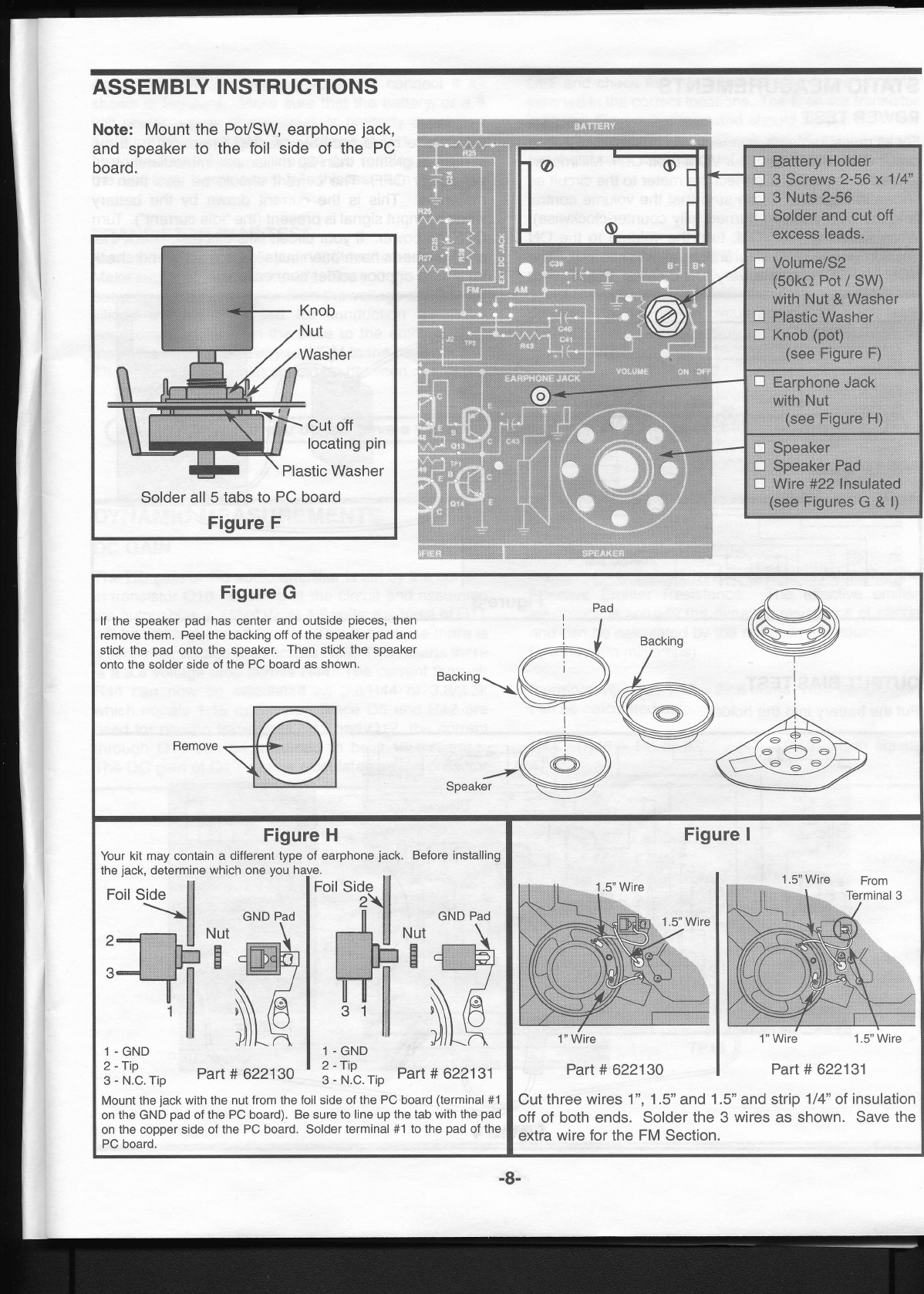
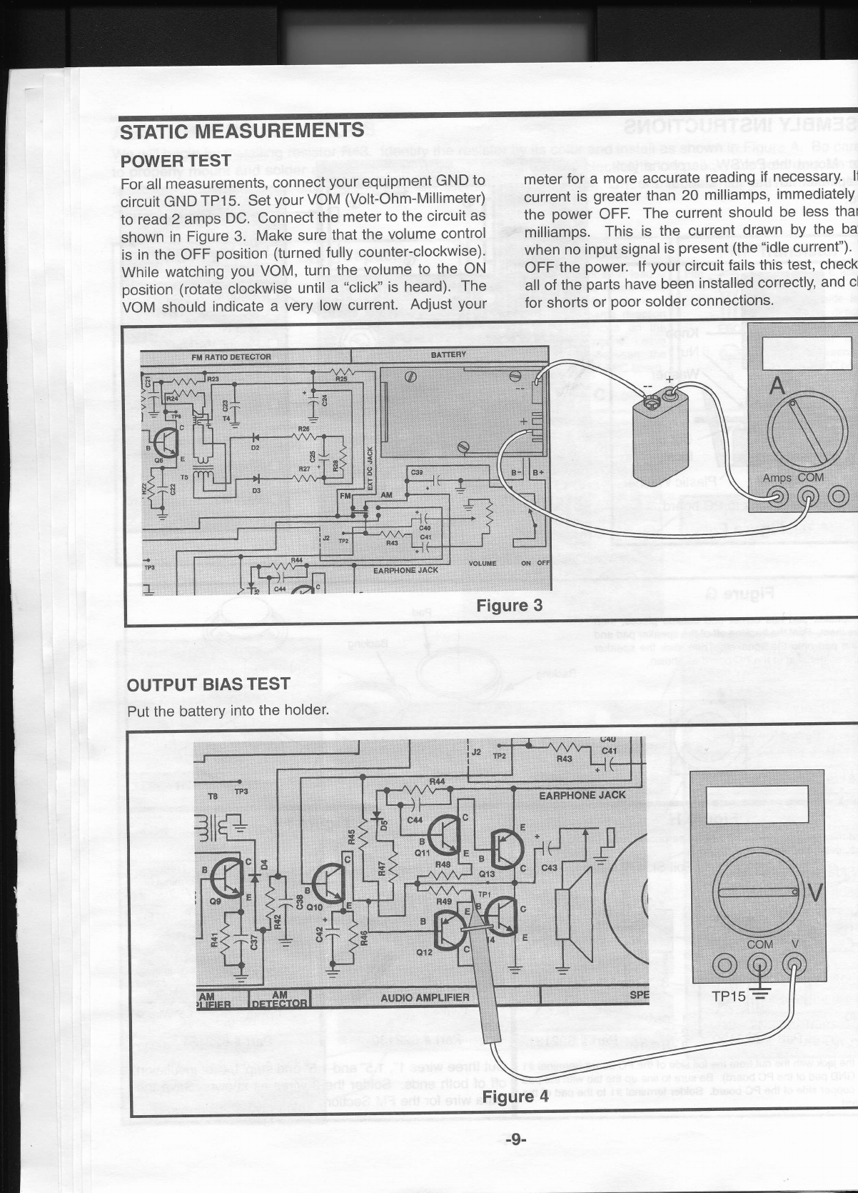
The purpose of section 1, the Audio Amplifier Stage, is to
increase the power of the audio signal received from the
detector to a power level capable of driving the speaker'
Section 2 includes the AM detector circuit and the AGC
(automatic gain control) circuit. The AM detector converts
it're amplitude modulated lF (intermediate frequency)
signal t<i a low level audio signal, lhe AGC stage feeds
bdck a DC voltage to the first AM lF amplifier in order to
maintain a near constant level of audio at the detector.
Section 3 is the second AM lF amplifier. The second AM
lF amplifier is tuned to 455kHz (Kilohertz) and has a fixed
gain at this frequency of 50. Section 4 is the first AM lF 2
Implifier which has a variable gain that depends on the
AGb voltage received from the AGC stage. The first AM
lF amplifiei is also tuned to 455k1z. Section 5 includes
the AM mixer, AM oscillator and AM antenna stages.
When the radio wave passes through the antenna, it
induces a small voltage across the antenna coil. This
voltage is coupled to the mixer, or converter, stage to be
changed to a frequency of 455kHz. This change is
accomplished by mixing (heterodyning) the radio
frequency signal with the oscillator signal. Section 6 it
FM ratio detector circuit. The FM ratio detector has a I
gain of about 20. Section 7 is the second FM lF ampl
The second FM lF amplifier is tuned to 10.71
(Megahertz) and has a set gain of approximately 2O'
3dB- bandwidth of this stage should be approximi
35OkHz. Section 8 is the lirst FM lF amplifier. The firs
lF amplifier is also tuned to 10.7MHz and has a set ga
approximately 10. lt also has a 3dB bandwidth of 350
Section 9 inciudes the FM mixer, FM oscillator, FM RF
the AFC circuits. The incoming radio waves are amp
by the FM RF amplifier, which is tuned to a desired t
siation in the FM frequency bandwidth of 88MH
108MHz. These amplified signals are then coupled tt
FM mixer stage to be changed to a f requency of 10.71
This change, as in AM, is accomplished by heterodl
the radio frequency signal with the oscillator signal'
AFC stage feeds back a DC voltage to the FM oscillal
prevent the oscillator from drifting. Each of these bl
will be explained in detail in the Theory of Operation 1
before the assembly instructions for that stage.

CONSTRUCTION
lntroduction
The most important factor in assembling your Superhet 1OB AM/FM Transistor Radio Kit is good soldering
techniques. Using the proper soldering iron is of prime importance. A small pencil type soldering iron of 25 -
40 watts is recommended. The tip of the iron must be kept clean at all times and well tinned.
Safety Procedures
. Wear eye protection when soldering.
' Locate soldering iron in an area where you do not have to go around it or reach over it.
' Do not hold solder in your mouth. Solder contains lead and is a toxic substance. Wash your hands
thoroughly after handling solder.
. Be sure that there is adequate ventilation present.
Assemble Components
In all of the following assembly steps, the components must be installed on the top side of the PC board unless
otherwise indicated. The top legend shows where each component goes. The leads pass through the
corresponding holes in the board and are soldered on the foil side.
Use only rosin core solder ol 63137 alloy.
DO NOT USE ACID CORE SOLDER!
What Good Soldering Looks Like
A good solder connection should be bright, shiny,
smooth, and uniformly flowed over all surfaces.
Foil Side
AA*l4al%n-
Mount Part I Bend Leads to I Solder and
Hold Part I Cut Olf Leads
Types of Poor Soldering Connections
1. Solder all components from
the copper foil side only.
Push the soldering iron tip
against both the lead and
the circuit board foil.
Apply a small amount of
solder to the iron tip. This
allows the heat to leave the
iron and onto the foil.
lmmediately apply solder to
the opposite side of the
connection, away from the
iron. Allow the heated
component and the circuit
foil to melt the solder.
Allow the solder to flow
around the connection.
Then, remove the solder
and the iron and let the
connection cool. The
solder should have flowed
smoothly and not lump
around the wire lead.
Here is what a good solder
connection looks like.
Circuit Board
Soldering lron
1. lnsufficient heat - the
solder will not flow onto the
lead as shown.
lnsufficient solder - let the
solder f low over the
connection until it is
covered. Use just enough
solder to cover the
connection.
Excessive solder - could
make connections that you
did not intend to between
adjacent foil areas or
terminals.
Solder bridges - occur
when solder runs between
circuit paths and creates a
short circuit. This is usually
caused by using too much
solder. To correct this,
simply drag your soldering
iron across the solder
bridge as shown.
Soldering iron positioned
incorrectly.
Component Lead
2.
2.
4.
Soldering lron
-4-

TS FAMILIARIZATION
This section will familiarize you with the proper method used to test the transistors and the diode'
TRANSISTOR TEST
Refer to the parts list and find a NPN transistor' Refer
the Figure C (page 7) for locating the Emitter, Base and
Colleclor. Using an Ohmmeter, connect the transistor
as shown in Test A. Your meter should be reading a low
resistance. Switch the lead from the Emitter to the
Collector. Your meter should again be reading a low
resistance.
Using an Ohmmeter, connect the transistor as shown in
Test b. Your meter should be reading a high resistance'
Switch the lead from the Emitter to the Collector' Your
meter should again be reading a high resistance'
Typical results read approximately 1MO to infinity'
DIODE TEST
Refer to the parts list and find a diode. Refer to Figure E
(page 7) for locating the Cathode and Anode' The end
*itn- tf'e band is the cathode' Using an Ohmmeter,
connect the diode as shown in Test E' Your meter
should be reading a low resistance' Using an
Refer to parts list and find a PNP transistor, refer
Figure D (page 7) for locating the Emitter, Base a
Collector. Using an Ohmmeter, connect the transis
as shown in Test C. Your meter should be r:eading a I
resistance. Switch the lead from the Emitter to I
Collector. Your meter should again be reading a I
resistance.
Using an Ohmmeter, connect the transistor as showt
Test D. Your meter should be reading a high resistan
Switch the lead from the Emitter to the Collector' Y
meter should again be reading a high resistance'
Ohmmeter, connect the diode as shown in Test F' '
meter should be reading a high resistance' Tyl
results read approximately 1Mo to infinity for sil
diodes (1N4148).
High Resistance
TEST ETEST F
-5-
Hioh Resistan
ilil
lm"lF
@
,) 1A<
\ / -.r'l
l\-7 //_
'a ./-
High Resistance
/ ttptt I
Low Resistance
\
/r*, t
'-,
+
++
+
TEST ATEST BTEST CTEST D

SECTION 1
The purpose of the Audio Amplifier is to in-crease the
audio power to a level sufficient to drive an g ohm
speaker. To do this, DC (direct current) from the battery
is converted by the amplifier to an AC (alternating
current) in the speaker. The ratio of the powei
delivered to the speaker and the power taken from the
battery is the efficiency of the amplifier. ln a Class A
amplifier (transistor on over entire cycle) the maximum
theoretical efficiency is .5 or 50%, but in a Class B
amplifier (transistor on for 1/2 cycle) the maximum
theoretical efficiency is .785 or 7B.So/o. Since transistor
characteristics are not ideal, in a pure Class B
amplifier, the transistors will introduce crossover
distortion. This is due to the non-linear transfer curve
near zero current or cutoff. This type distortion is
shown in Figure 2.
ln order to eliminate crossover distortion and maximize
efficiency, the transistors (Q11 and e12) of the audio
amplifier circuit are biased on for slighily more than 1/2
of the cycle, Class AB. ln other words, the transistors
are working as Class A amplifiers for very small levels
of power to the speaker, but they slide toward Class B
operation at larger power levels.
Transistor Q10 is a Class A amplifier that drives e11
and Q12 through the bias string R44, D5 and R47. elg
and Q14 are current amplifiers that amplify the current
of transistors Q11 and Q12. The AC and DC gain are
set by the DC current in transistor e10 and the collector
resistor R44. The AC gain of the Audio Amptifier is
approximately equal to 100, while the DC gain equals
approximately 50. The transistors e13 and e14 self
bias so that the voltage at their emitters is
approximately 1/2 the supply voltage. R45 provides
feedback to the base of e10 which is biased at
approximately .7 volts. Capacitor C40 couples the
audio signal from the volume control to the input of the
audio amplifier. Capacitor C43 btocks the DC to the
speaker, while allowing the AC to pass.
Figure 2
-6-

ASSEMBLY INSTRUCTIONS
We will begin by installing resistor R43. ldentify the resistor by its color and install as shown in Figure A. Be ca
to properly mount and solder all components. Diodes, transistors and electrolytic capacitors are polarized, be
to follow the instructions carefully so that they are not mounted backwards. Check the box when you have compl
each installation.
Test Point Pin
l-ol
_il-
Foit side )y'
of PC Board
Figure A
Lytic Capacitor
Polarity Mark
Be sure that the negative lead is in
the correct hole on the PC board.
Figure B
FIaI
Side
NPN
F
nT[
ililil
l]l]U
EBC
B
6"
Transistor
Mount so E lead is
in the arrow hole
and flat side is in
the same direction
as shown on the
top legend. Leave
1/4" between the
part and PC board.
Figure G
P Transistor
Mount so E lei
in the arrow
and flat side
the same dire
as shown on
^ top legend. Lr
v 1/4" between
part and PC bo
Figure D
DiOde , Band
/
6, Il;:"0*"
Be sure that the
band is in the
correct direction. -+t--
Figure E
tr Q13 - MPS6562 or eSsO
Transistor, (see Figure D
-7-

ASSEMBLY INSTRUCTIONS
Note: Mount the PoVSW, earphone jack,
and speaker to the foil side of the PC
board.
Knob
Nut
Washer
Cut off
locating pin
Plastic Washer
Solder all 5 tabs to PC board
Figure F
Figure G
lf ihe speaker pad has center and outside pieces, then
remove them. Peel the backing off of the speaker pad and
stick the pad onto the speaker. Then stick the speaker
onto the solder side of the PC board as shown.
Figure H
Your kit may contain a different type of earphone jack. Belore installing
Backing
A
K@))
NZ
Cut three wires 1", .1.5" and '1.5" and strip 1/4" of insulation
off of both ends. Solder the 3 wires as shown. Save the
extra wire for the FM Section.
Figure I
the jack. determine which one yo, hu,u1 .. _. . '
Foir side [l lroit siolll
\.ll GND Pad I tt tl
2-={----Lll r.r_,t _\ I r-tL1.U *_",
:4u;ffi1 ffi-
1 -GND
2 -rip
3 - N.C. Tip Part # 622130
1"Wire
Part # 622130
'1" Wire 1.1
Part # 622131
GND Pad
d
Nd
1 -GND
3 -li% t'o Part # 622131
Mount the jack with the nut from the foil side of the PC board (terminal #1
on the GND pad of the PC board). Be sure to line up the tab with the pad
on the copper side of the PC board. Solder terminal #1 to the pad of the
PC board.
GND Pad
1.5" Wire
-8-

STATIC MEASUREMENTS
POWER TEST
For all measurements, connect your equipment GND to
circuit GND TP15. Set your VOM (Volt-Ohm-Millimeter)
to read 2 amps DC. Connect the meter to the circuit as
shown in Figure 3. Make sure that the volume control
is in the OFF position (turned fully counter-clockwise)'
While watching you VOM, turn the volume to the ON
position (rotate clockwise until a "click" is heard). The
VOM should indicate a very low current. Adjust your
OUTPUT BIAS TEST
Put the batterY into the holder.
meter for a more accurate reading if necessary. 11
current is greater than 20 milliamps, immediately
the power OFF. The current should be less that
milliamps. This is the current drawn by the ba
when no input signal is present (the "idle current").
OFF the power. lf your circuit fails this test, check
all of the parts have been installed correctly, and cl
for shorts or poor solder connections'
ra P3
?l ff
K
..';.
O
Ia
-1 r0
r+
{-
o'
Figure 4

Adjust your VOM to read 9 volts and connect it as
shown in Figure 4. Make sure that the battery, or a 9
volt power supply (if available), is properly connected
and turn the power ON. The voltage at TP1 should be
between 3 to 6 volts. lf you get this reading, go on to
the next test. lf your circuit fails this test, turn the power
TRANSISTOR BIAS TEST
Move the positive lead of your VOM to the base of Q11.
Make sure that the power is ON. The voltage should be
between .5 and .8V higher than the voltage at TP1. All
silicon transistors biased for conduction will have
approximately .7V from the base to the emitter. Now
move the positive lead of your VOM to the base of Q12.
The voltage at this point should be between .5 and .8V
OFF and check that all of the transistors are correctly
inserted in the correct locations. The E on the transistor
indicates the emitter lead and should always be in the
hole with the E next to it. Check that all resistor values
are the correct value and not interchanged.
lower than the voltage at TP1. This is because Q12 is
a PNP type transistor. Turn the power OFF. lf your
circuit fails this test, check the Q11 and Q12 are
properly inserted in the circuit board. All static tests
must pass before proceeding to the Dynamic Tests or
the next section.
lf you do not have a variable power supply, skip to the next test.
DYNAMIC MEASUREMENTS
DC GAIN
The DC gain of the audio amplifier is set by the current
in transistor Q10. Looking at the circuit and assuming
the output bias is 112 of V+ or 4.5 volts, the base of Q11
will be .7V higher or 5.2 volts. This is because there is
a negligible voltage drop across R4B. This means there
is a 3.8 voltage drop across R44. The current through
R44 can now be calculated as 3.8/R44 or 3.8/3.3k
which equals 1.15 milliamps. Since D5 and R42 are
used for biasing transistors Q11 and Q12, the current
through Q10 can be assumed to be 1.15 milliamps.
The DC gain of Q10 can be calculated as the collector
resistor, R44, divided by the emitter resistor plus the
Effective Emitter Resistance. The effective emitter
resistance is actually the dynamic resistance of silicon
and can be calculated by the approximate equation:
Rj = 26 / l(in milliamps)
therefore, Rj = 26 I 1.15 = 22.6 ohms. Now the DC gain
can be calculated as:
R44 / (R46 + Rj) or 3300 / @7 + 22.6) which equals
47.4.
Figure 5
-10-

It is advisable to use a digital meter because of the
small voltage changes in the following test. Connect
your VOM to the circuit as shown in Figure 5. Set your
VOM to read 1 volt DC and turn the power ON. Record
the base of Q10 here:
Turn the radio ON and turn the power suppl
lncrease the supply voltage until the voltage at .
equal to Vo. Now increase the voltage of the r
until the voltage at Tp1 decreases by i volt. Mo
positive lead of your VOM to the -base of e1
record the voltage here:
vb1 =volts.
Now set your VOM to read 9 volts and connect the
po.sitive lead to test point Tp1. Record the output bias
voltage here:
Vo - _ volts.
Turn the power OFF. With a 1M ohm resistor (brown_
black-green-gold), R34, connect the power supply to the
circuit as shown in Figure 6.
vb2 =
It may be necessary to change scales of your V(
a more accurate reading. Turn the power OFI
disconnect the power supply. Since the DC gain e
the DC change at the output divided by the DC cl
at the input, the DC gain of the audio can be calcr
as: 1 / (Vb2 - Vb1). your answer should be nei
calculated DC gain of 47.4.
Figure 6
do not h"u" "n "rdio gto Section 2.
AC GAIN
The AC gain can be calculated in the same manner as
the DC gain except for two differences. For AC,
capacitor C42 bypasses the emitter resistor R46
leaving only the effective emitter resistance, and there
is a resistance seen at the output of e13 and e14. The
AC gain of Q10 can be catcuiated as R44 / Rj or 3300
/ 226 which equals 146. When the input signal is
positive, there will be a current flowing in e11, wh-ich we
will call l(O11). This current wiil theh be muttiptied by
the Beta (B) of transistor e13 or B x t(O11). fhe totat
current at the output is equat to t(e11) x (1 + B). The
resistance of R4B is also seen at the output. The
resistance is effectively divided by 0, R4B / B.
Assuming B of the output transistors are equal to 100
than the resistance seen at the output is equal to 1
ohm, 100 / 100. This means that there is a voltage
divider between the output and the g ohm speaker. The
signal is now divided down so that the output is equal
to the AC (gain of e10) x (B / (1+8)), or 146 x 1e i Sy
which equals 130. This is also true when the inpui
signal is negative. The only difference is that e12
Q14 are now conducting. Connect the VOM and a
generator to the circuit as shown in Figure 7.
Normally the AC gain is measured at a frequenc
1kHz. Your VOM, however may not be ablr
accurately read AC voltages at this f reque
Therefore, it is recommended that this test
performed at 4O0Hz. Set the audio generator at 40
and m-inimum voltage output. With the power ON,
your VOM to read an AC voltage of 1 volt at test p
TP1. lncrease the volume Control about half r
Slowly increase the amplitude of the audio gener
until your VOM reads 1 volt AC. Leave the at
generator at this setting and move the positive lear
your VOM to the base of e10. Record the ,AC ir
voltage to the amplifier here:
-1 1-
Vin =volts.

You may have to change scales on your VOM for the
most accurate reading. Turn the power OFF. The AC
voltage gain of your audio amplifier is equal to the AC
output voltage divided by the AC input voltage, or 1/Vin.
The gain should approximately equal the calculated
gain.
Figure 7
lf an oscilloscope is not available, skip the following test and go directly to Section 2.
AC BANDWIDTH
Oscilloscope
Figure 8TP15
Connect the oscilloscope and audio generator to your
circuit as shown in Figure 8.
Set the audio generator for a frequency of l kHz and
minimum voltage output. Set the oscilloscope to read
.5 volts per division. Turn on the power and slowly
increase the volume control to a comfortable level.
lncrease the amplitude of the audio generator until the
oscilloscope displays 2 volts peak to peak, (Vpp), at
TP1. lt may be necessary to adjust the volume control.
Move the oscilloscope probe to the base of Q10 and
record the input voltage here:
(at this point, you may want to verify the AC gain).
Move the oscilloscope probe back to TP1 and slowly
increase the frequency from the audio generator until
the waveform on the oscilloscope drops to .7 of its
original reading (1.aVpp or 2.8 divisions). The
frequency of the generator, when the output drops to
.7 of its original value, is called the high frequency 3
decibel (dB) corner. Record this frequency here:
Vin =Vpp -12-
(f high 3dB) =kHz.

Slowly decrease the frequency of the generator until
the output drops to .7 of its original reading, 1.4Vpp or
2.8 divisions. This frequency is called the low
frequency 3dB corner - the low frequency 3dB corner or
(f high 3dB) - (f low 3dB). Your calculated answer
should be greater than 30kHz.
DISTORTION
Connect the generator and oscilloscope as shown in
Figure 8. Set the generator at a frequency of 1kHz, turn
the power ON and turn the volume to maximum. Adjust
the generator output until the peaks of the sinewave at
TP1 are clipped as shown in Figure 9A. One side of the
sinewave may clip before the other depending on the
DC centering at TP1. lf oscillations are seen, connect
a clip lead from the GND of your generator to the GND
of the circuit.
Figure 9
Measure the maximum voltage peak to peak when
clipping first occurs and record that value here:
Vclp =Vpp.
Using a wire short out diode D5 and resistor R47 as
shown in Figure 10. The waveform should resemble
Figure 98. The "flat spots" near the center of each
sinewave demonstrate what is called crossover
distortion. Most of this distortion should disappear when
you remove the shorting lead. Turn the power OFF.
Wire Lead
or Clip Lead
Figure 10
MAXIMUM POWER OUTPUT
The maximum power output before distortion d
"clipping" can be calculated using the voltage
obtained in step 4 as follows:
Vpeak (Vp) = Vclpl2
Vroot mean squared (Vrms) = Vp x .7
Max power out = (Vrms)'/B ohms = (Vclp x .l
Maximum power output should be greater thar
milliwatts.
EFFICIENCY
By measuring the DC power taken from the battt
the maximum power output level, the efficiency I
audio amplifier can be calculated. Power fror
battery is equal to the current taken from the b
times the voltage of the battery during maximum 1
output. Efficiency can then be calculated as follow
= Max audio power/Battery power. lt is best to
power supply (if available) to prevent supply v<
from changing during these measurements. Co
the generator, oscilloscope and current meter as s
in Figure 11. Set your current meter to read 1 am
Turn the power ON and rotate the volume conl
maximum. Slowly increase the amplitude of the
generator until the output is clipped as shown in F
9A. Record Vclp here:
Vclp =vpp.
This should be equal to Vclp in step 4. Record tl
current drawn from the 9 volt supply here:
Current (l) max =Amps.
Measure the supply voltage and
here: record the V s
V supply =volts.
Turn the power OFF. Calculate the maximum
output as done in the Maximum Power Output Stt
Record your answers on the next Pag
-13-

lf you do not have a power supply, use a 9
volt battery instead.
Figure 11 TP15
Max power out =
Since the battery power equals the battery voltage times the current taken from the battery; calculate the battery
power:
Battery power = lmax x V supply Battery powor =
Since the efficiency (N) is equal to the Max power out divided by the Battery power, we can now calculate the
efficiency of the audio amplifier.
Vp = vclp/2
Vrms=Vpx.7
Max power 6u1= (Vrms)'z/8
N = Max power ouVBattery power
Nin%-Nx100
vp=
Vrms =
N-
\|=
Your calculated answer should be around .6 or 60%.
-14-
o/
/o

SECTION 2
AM DETECTOR AND AGC STAGE
The purpose of the detector is to change the amplitude
modulated lF signal back to an audio signal. This is
accomplished by a process called detection or
demodulation. First, the amplitude modulated lF signal
is applied to a diode in such a way as to leave only the
negative portion of that signal (see Figure 12). The
diode acts like an electronic check valve that only lets
current pass in the same direction as the arrow (in the
diode symbol) points. When the diode is in conduction
(On Condition), it will force the capacitors C33 and C38
#,,
lT8
t
Figure 12
The purpose of the automatic gain control (AGC) circuit
is to maintain a constant level at the detector,
regardless of the strength of the incoming signal.
Without AGC, the volume control would have to be
adjusted for each station and even moderately strong
stations would clip in the final lF amplifier causing audio
distortion. AGC is accomplished by adjusting the DC
bias of the first lF amplifier to lower its gain as the signal
strength increases. Figure 12 shows that the audio at
the top of the volume control is actually "riding" on a
negative DC voltage when strong signals are
'tar
W
?:i
to charge to approximately the same voltage as
negative peak of the lF signal. After conduction sl
in the diode (Off Condition), the capacitors
discharge through resistors R36 and R42.
discharge time constant must be small enough to fo
the audio signal or high frequency audio distortion
occur. The discharge time constant must be li
enough, however, to remove the intermed
frequency (455kHz) and leave only the audio as sh
in Figure 12.
VOLTS
encounlered. This negative DC compor
corresponds to the strength of the incoming signal.
larger the signal, the more negative the componenl
test point five (TP5), the audio is removed by a low I
filter, R36 and C32, leaving only the DC compor
Resistor R35 is used to shift the voltage at TP5
enough to bias the base of transistor QB to the full
position when no signal is present. Resistors R35
R36 also forward bias diode D4 just enough to minir
"On Condition" threshold voltage.
I
ASSEMBLY INSTRUCTIONS
-15-

ASSEMBLY INSTRUCTIONS
Check that the VOM is adjusted to
read 9 volts DC and turn the power
ON. The voltmeter should read
approximately 1.5 volts DC. lf your
reading varies by more than .5 volts
from this value, turn the power OFF
and check the polarity of D4. Also
check R36 and R35 and check that
transformer T6 is properly installed.
STATIC MEASUREMENTS
AGC ZERO SIGNAL BIAS
With the power turned OFF, connect your VOM to TPS as shown in Figure 13. Make sure that the AM/FM switch is
in the AM position.
Figure 13
T8 TEST
With the power turned OFE connect the positive lead of
the VOM to TP3 and the negative lead to ground pin
TP15. Make sure that the VOM is set to read 9 volts DC
and turn the power ON. The voltage on the VOM should
be the same as your battery voltage or power supply
voltage. lf not, turn the power OFF and check that TB
is properly installed. Turn the power OFF.
lf you do not have an RF generator, skip to Section 3.
-16-

ffiUREMENTS
AM DETECTOR AND AGC TEST
Connect yourVOM and RF generator as shown in Figure 14'
TP1 5
Figure 14
Set the VOM to accurately read 2 volts DC and set the
""tprt of the RF generator for 455kfz' no .T*li:":
anO minimum voltage output' Turn the power ON and
rio*fy increase the amplitude of the generator until the
SYSTEM CHECK
Connect your equipment as shown in Figure 15'
voltage at TP5 just starts to droP'
the AGC threshold with no lF gain'
amplitude setting on the RF
lf your RF generatfA;es not have amFlitude modulation and
-' ' you O-o not have an oscilloscope' skip to Section 3'
This point is ca
Make a note of
generator ht
Oscilloscc
TP1 5
lf this test failt
and TPS. Tu
.001pF
TP15 Figure 15
Set the RF generator at 455kHz ' lk1z at B0%
modulationandminimumvoltageoutput.Turnthepower
ON anO set the volume contiol at maximum' Slowly
aOlust the amplitude of the RF generator output until you
hear the l kHz tone on the sPeaker'
the power OFF and check R42, D4
power OFF.
-17-

AM DETECTOR BANDWIDTH TEST
Connect your test equipment as shown in Figure 15.
Set the generator at 455kHz with 80% modulation at a
modulation frequency of 1kHz. Set the oscilloscope to
read .1 volts per division. TUrn the power ON and set
the volume at the minimum. lncrease the amplitude of
the generator until the signal on the oscilloscope is 4
divisions peak to peak. Check the signal to make sure
that it is free of distortion. Leave the frequency of the
generator at 455kHz, but increase the modulation
frequency until the output drops to .28Vpp. Record the
modulation frequency on the generator here:
This frequency should be greater than SkHz. Turn the
power OFF.
SECTION 3
SECOND AM IF AMPLIFIER
The purpose of the second lF amplifier is to increase
the amplitude of the intermediate frequency (lF) and at
the same time provide SELECTIVITY. Selectivity is the
ability to "pick out" one radio station while rejecting all
others. The second lF transformer (T8) acts as a
bandpass filter with a 3dB bandwidth of approximately
6kHz. The amplitude versus frequency response of the
second lF amplifier is shown in Figure 16.
Both lF amplifiers are tuned to a frequency of 455k{z
and only need to be aligned once when the radio is
assembled. These amplifiers provide the majority of the
gain and selectivity needed to separate the radio
stations.
The gain at 455kHz in the second lF amplifier is fixed
by the AC impedance of the primary side of transformer
T8, and the DC current in Q9. The current in Q9 is set
by resistors R39, R40 and R41. Both C36 and C37
bypass the 455kHz signal to ground, making Qg a
common emitter amplifier. The signal is coupled from
the lirst lF amplifier to the second lF amplifier through
transformer T7. The lF transformers not only supply
coupling and selectivity, they also provide an
impedance match between the collector of one stage
and the base of the next stage. This match allows
maximum power to transfer from one stage to the next.
.707
452kHz
445 458kHz -*
465 -- Over all lF Gain
Single stage lF Gain
455kHz
Figure 16
-18-

ASSEMBLY INSTRUCTIONS
i':ili:oA7t,ti.::li ,..{e$S},l,'.:l.:l,t
or .3?2vF {22.3) Disr
STATIC MEASUREMENTS
Q9 BIAS
Connect your VOM as shown in Figure 17. Set the
VOM to read 9 volts DC and turn the power ON. The
voltage at the emitter of Q9 should be approximately 1
volt. lf your reading is different by more than .5
turn the power OFF and check components R39
R41 and Q9.
Figure 17
lf you do not have an RF generator and oscilloscope, skip to Section 4.
-19-
Other manuals for AM/FM-108TK
1
Table of contents
Other Elenco Electronics Radio manuals

Elenco Electronics
Elenco Electronics MX-901C User manual

Elenco Electronics
Elenco Electronics AM/FM-108K User guide

Elenco Electronics
Elenco Electronics MX-901SW User manual

Elenco Electronics
Elenco Electronics AM-780K User guide

Elenco Electronics
Elenco Electronics MX-901AF User manual

Elenco Electronics
Elenco Electronics SCP-12 User manual

Elenco Electronics
Elenco Electronics MX-901F User manual

Elenco Electronics
Elenco Electronics FM-88K User guide

Elenco Electronics
Elenco Electronics SUPERHET AM-550TK User guide

Elenco Electronics
Elenco Electronics AM-550CK User guide