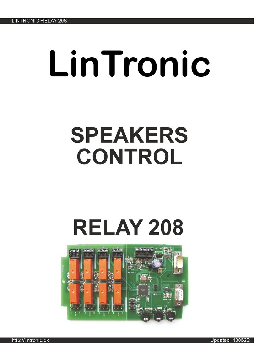
Emco EE301-T User manual

I INTRODUCTION
EMCO’sSolidStateVoltageRegulatingRelayTypeEE301-Tisusedforregulatingthesecondary
voltage of power transformer with on-load tap changer .The required dead-band settings are set
by setting the Nominal value and L & R levels independently.TheTime Delay setting on the front
panel eliminates the relay operations for momentary fluctuations of the regulated voltage, thus
reducing the number of operations of the tap changer.
When the regulated voltage falls below the specified Under Voltage limit, the control relays are
automatically blocked i.e. there is no voltage correction, and a pair of relay contacts is made
availableforalarm.
When the regulated voltage goes above the specified Over Voltage limit, the control relays are
automatically blocked i.e. there is no voltage correction, and the same pair of relay contacts (for
UV)ismade available for alarm.
A built-inTap Position Indicator with 1KWstep resistance can be provided optionally to indicate
theTap No.of the PowerTransformer upto a maximum of 35.
The relay uses all solid state circuitry which increases its reliability and life. The output, input
connectionsaremadethroughaterminalblock. However all normal precautions/care in handling/
storageshould be observed asfor a sensitive electronicinstrument.
II GENERAL DESCRIPTION
EMCO'sSolidStateAutomaticVoltage Regulating RelayTypeEE301-Tisdesigned formaximum
operational simplicity. It regulates the secondary voltage of power transformers with on-load
tapchangers. The bandwidth control allows the dead-band to be set in terms of upper (LOWER
VOLTS)andlower(RAISEVOLTS) voltagelimits around a particular nominal value withspecified
sensitivity.
The Time Delay control allows the regulator to respond only to voltage fluctuations lasting for
periodsgreaterthan the selected time delay.Where the voltagecorrectionrequiresmorethanone
tap change, the time delay is re-initiated before further tap changes. No special provisions are
requiredtoresetthetimedelaywhich resets automatically after the voltage correction. SolidState
Lamps (LEDs) indicate voltage outside the preset limits and control relay operations.
Operation of the RAISE / LOWER Control Relay is automatically inhibited when the voltage falls
below the specified undervoltage limit or goes above the Overvoltage limit. One pair of normally
open relay contacts are provided to effect the tapchanger RAISE and LOWER operations and to
trigger an alarm in case of Undervoltage / Overvoltage conditions. (Only one pair of contacts is
availableforeitherUV or OV)
Analarmintheformofnormallyopencontactsis providedincaseof control failurei.e.AVR Relay
continuouslyshowingeither'L' or 'R' command formorethan 15 minutes due tomalfunctioningof
AVR/OLTC/ anyreason.
A built-inTap Position Indicator with 1KWstep resistance can be provided optionally to indicate
theTap No.of the PowerTransformer upto a maximum of 35.
1

III SPECIFICATIONS
Auxiliary Supply.................... 110V/230V AC + 15% 50Hz, 15VA
PT Supply ........................... 110V AC 50Hz, 1.5VA and readable on display
NominalValue Setting (NVA).... Adjustable between 110V + 10% & readable on display
LOWER Volts Setting............. Adjustable between 0.5V to 5V above
the NVA and readable on display
RAISE Volts setting................ Adjustable between 0.5V to 5V below the
NVA and readable on display
Time Delay Setting................... Fixed(VoltageIndependent)Time
Delay adjustable from 10 to 120 Secs
Time Delay Resetting.............. Instantaneousresettingwithvoltage
returningtodeadband
Undervoltage Blocking............. Internal blocking at 80% of regulated value.
Restorationat85% of regulated value
Overvoltage Blocking.............. Internal Blocking at 132V & Restoration at 127V
Control Relays........................ One pair of normally open potential free contacts of
rating 5A at 240V AC or 24V DC resistive load for each
Lower, Raise, Control Fail & Undervoltage / Overvoltage
control relays (Only one pair of contacts is available for
either UV or OV)
Control Operation.................... Single Pulse operation with approx. 2 secs on time
OperatingTemperature............. 0°C-45°C
Overall Size........................... 378mmX 160mm X 260mm (HX W X D)
Weight.................................... 5 Kgs. (approx.)
Options.................................. 1. TapPositionIndicator,Max.35Taps with 1KWresistance
2. Line drop compensator with resistive and reactive
compensation of either polarity upto 20% and
suitable for operation with 1A, 5VA current
transformer
3. Normally closed Auxiliary Supply Fail Relay Contacts
4. User defined settings for PT Supply, Time Delay,
Undervoltage & Overvoltage Blocking. User specified
step resistance for TPI
5. 4-20 mA TPI output for SCADA
2

IV. FAMILIARIZATION WITH VARIOUS INDICATIONS / CONTROLS :
A. INDICATIONS
1.4x7 Segment Display (AVR) : Display lights when Auxiliary Supply is 'ON'.
2. 2x7 Segment Display (TPI) : Display lights when Auxiliary Supply is 'ON'.
3.‘L’Lamp : ‘ON’ whenever the PT voltage exceeds the 'LOWER
VOLTS’ set limit.
4. ‘R’ Lamp : ‘ON’wheneverthePTvoltage falls below the ‘RAISE
VOLTS’ set limit.
5. UV / OV Lamp : 'ON’ whenever the PT voltage falls below the factory
set Undervoltage limit i.e. below 80% of the Nominal
voltage. This lamp will turn-off only when the PT
voltageraisesabove85%oftheNominalvoltagevalue.
This lamp will also be ‘ON’, when the PT voltage goes
above the factory set Overvoltagelimit i.e.above132V.
This lamp will turn-off only when the PT voltage falls
below127V.
6. 'LR' Lamp : 'ON'whenLowerRelayis energised.
7. ‘RR’ Lamp : ‘ON’when Raise Relay is energised.
8. 'CF' Lamp : 'ON'whenControlFailRelayisenergised,i.e.whenthe
PTvoltageremainsoutside the bandwidthformorethan
15 minutes.
9.‘TEST’ Lamp : ‘ON’when AVR is in “TEST”mode.
B. CONTROLS
1. Power - ON : This is a toggle switch which when’ON’ supplies
Auxiliary Voltage to the instrument.
2. 'R’ Set : This is a variable control varying from 0.5V to 5.0V below
NVA setting.This control sets the (lower limit of the PT
voltage below which if the voltage reduces, then
corrective action will be taken by the instrument. The
setting is to be read on display.
3. 'NOM’ Set : This is a variable control to set the Nominal value of
PT voltage varying between + 10% of 110V. This set
ting becomes the reference level around which L & R
setting can be varied. The setting is to be read on the
display.
4. 'L’ Set : This is variable control, varying from 0.5V to 5.0V
above NVA setting.This control sets the upper limit of
the PT voltage beyond which if the voltage rises,
corrective action will be taken by the instrument.
The setting is to be read on display.
3

5.Time Delay : Corrective action takes place only after the Time
Delay as set by this control has elapsed and the
PTVoltagecontinues to remain outside the set
Lower or Raise limits (but does not fall below the
UV / OV limit).
6.Test/Normal Switch for AVR : It selects theTest or Normalmodeofoperation.In
theTest mode, PTVoltage is simulated internally
& can be varied through the Test Control on the
front panel. An LED indication is provided to
indicatethat the instrumentis inTest mode.In the
Test mode, the control relays are “cut off” so that
undesired operation of OLTC is prevented during
testing.Thevoltageis monitored on the displayin
PT I/P position. In the Normal mode external PT
voltage gets connected to the instrument.
Thisswitch must be kept in ‘’Normal” mode when
the instrument is in use.
7.Test Voltage Control : Simulates PT I/P inTest mode and can be varied
from 0V to 150V AC.
8.Test / Normal Switch for TPI : In the Test mode, display indicates "88" for
checking the display. In Normal mode it displays
the actual tap no. of OLTC.This switch must be
kept in "Normal" mode.
9. Selector Switch : Selectsthevoltagesetting to be monitored onthe
display. It also enables the PT voltage to be read
on the display.
NOTE : Before connecting Aux. Supply & PT Supply to the AVR Relay, Check-up
following points.
A) Mechanical Damage : Remove the front acrylic cover by removing the
thumbscrews & check for any mechanical damage to the unit.
B) Aux fuse & PT fuse (on Rear Panel) : Note that Aux. fuse is 300mA (20mm)
& PT fuse is 100mA (20mm). Do not interchange these fuses. Check them &
replacewithgood ones if required.
4

V. OPERATING INSTRUCTION :
1. Check the PT & Auxiliary fuses.
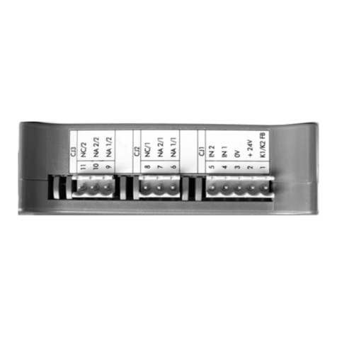
2. Connect 110V / 230V A.C.Aux.Supply to pins 1 & 2 of the Rear PanelTerminal
Block.
3. Connect PT Supply to pins 3 & 4 of the Rear PanelTerminal Block.
4. Turn on the instrument by putting Power Switch to 'ON' position.
5. Leave the unit on for 15 minutes before making any settings.
6. Check theTest / Normal Switch is in the Normal mode.
7. Make the following settings by changing selector switch.
NOMINALVALUE 110V
LOWER VOLTS Setting 112V
RAISE VOLTS Setting 108V
TIME-DELAYSetting 30 Sec.
%R & %X Setting ‘0’ %
(in case of relay with LDC)
8. Keep the selector switch to PT I/P position.
9. Increasethe PT voltageto read PT= 110V
10. Note that under this condition all the lamps viz. L, R, LR, RR & UV/OV are off.
11.LOWERVOLTS OPERATION CHECK :
Increase the PT Supply above 112V (atleast 112.5V), but ensure that it is below
OV limit (132V). 'L' lamp should immediately turn on.
The'LR' control pulse will come only after30 secs. fromthe instant ofturning on
of 'L' lamp. The control pulse will remain 'ON' for 2 secs, after which the Time
Delayof 30 secs. willrestart & the controlpulse will come again for 2 secs.& the
cycle is repeated. Check the LR contacts on pins 9-10 of the Rear Panel
Terminal Block.
12.RAISEVOLTS OPERATION CHECK :
DecreasethePTSupplybelow 108V (atleast 107.5V), but ensurethatitis above
UV limit (88V). 'R' lamp should immediately turn on.
The'RR'control pulse will comeonly after 30 secs.from the instant ofturningon
of 'R' lamp. The control pulse will remain 'ON' for 2 secs, after which the Time
Delayof 30 secs. will restart & thecontrol pulse willcome again for2 secs. & the
cycle is repeated. Check the RR contacts on pins 11-12 of the Rear Panel
Terminal Block.
5

NOTE: Please note that for the operational safety, RAISE and LOWER relays are
interlocked and hence OLTC will never receive two opposite commands
simultaneously.
13.UNDERVOLTAGE OPERATION CHECK :
Reduce PT Supply below 88V (atleast 87.5V) (UV is factory set at 80% of the
Nominalvoltage),UV/OVlamp will turn-onimmediatelly.(Under this condition R
lamp will also be on) but the Raise control is inhibited. Note that between
Blocking&Release (Restoration), a hysteresis of5% has been provided. Check
the UV contacts on pins 13 & 14 of the Rear Panel Teminal Block.
Raise the PT Supply above 94V, UV/OV lamp should turn off immediately.
'R'lamp indication however shall remain on, if the PT voltage is still below the
Raise setting.The raise control pulse comes on after the set time delay.
Disconnect external PT supply the UV/OV & Rlamp will turn on immediatelly.
TheUV/OV relaywilloperate.Afterrestoration of PT supply,thelampwillturn'off'
& UV/OV relay will be deenergised.
NOTE: Blocking(80%)&Restoration(85%) are factory setvalues,unless the customer
hasspecifiedothervalues.
14.OVERVOLTAGE OPERATION CHECK :
Increase PT Supply above 132V (atleast 132.5V), UV/OV lamp will turn-on
immediatelly.(Underthis condition L lamp willalsobe on) buttheLowercontrolis
inhibited. Note that between Blocking & Release (Restoration), a hysteresis of
5V has been provided. Check the UV/OV contacts on pins 13 & 14 of the Rear
Panel Teminal Block.
Decrease the PT Supply below 127V, UV/OV lamp should turn off immediatelly.
'L' lamp indication however shall remain on, if the PT voltage is still above the
Lower setting.The lower control pulse comes on after the set time delay.
NOTE: Blocking (132V) & Restoration (127V) are factory set values, unless the
customerhas specified other values.
15.CONTROL FAIL ALARM RELAY :
ChangethePTvoltagetogeteitherRorLindication.Keepthe regulated voltage
outsidethesetdeadband.After15minutes(approx.).thecontrolfailalarmrelay
will operate and will remain in energised condition till the voltage returns to set
deadband.This operation will beindicated by red LED marked CF mounted on
front panel of AVR Relay.The relay contacts can bechecked on Pins 15 & 16 of
the Terminal Block.
Take the regulated voltage within set dead band.The control fail Relay will get
deenergised and the contacts on Pins 15 & 16 will open and CF LED
will stop glowing. Similarly this operation can be checked by taking regulated
voltageon other sideof set deadband
6

16. TEST MODE :
When the 'Test / Normal' switch is put in the 'TEST' mode, the PT I/P can be
simulated through the 'TEST Control'. However to prevent any undesirable
operation of the OLTC, the relays are cut off, but the lamp indications are
available.
17. TIME DELAY :
This is a variable control with variation from 10 sec. to 120 sec. The actual
setting can be made as required. The corrective action will take place only after
the set Time Delay interval is elapsed provided the voltage deviation persists
evenafterthesetTimeDelayandthattherelayisnotoperatinginUV / OV mode.
18. CONTROLRELAYS :
Connect the respective Lower, Raise, Control Fail and Under / Over voltage NO
contacts to operate the respective contactors / Alarms.
19. TPIOPERATION CHECK :
Keep the Test/Normal Switch of TPI in Normal mode & connect Min., Max. &
WiperfromOLTC to the Rear PanelTerminalBlock.Changethetappositionfrom
1 to maximum tap and check whether TPI reads correctly.
Keep the TPI "Test/Normal" switch in "Test" mode & check whether
display reads "88".
FUSE REPLACEMENT:
1 After switching power-on, the display indication must come. If it does not come,
check whether AUX. fuse on the rear panel is properly tightened. If the
instrument still does not work, unscrew the fuse & check if it is open. Replace
it by another fuse of 300mA (20mm).
Once again ensure that the fuse is not loose. The instrument should turn on
now. If the fuse keeps on blowing repeatedly or the instrument does not work
inspite of good fuse, proceed to identify the faulty PCB as given in fault finding
procedureVII.
2 Connect the PT supply and put the Test/Normal switch in Norrnal position. If
the Instrument is turning on but you are continuously getting 'R’ and ’UV’
indication, check whether PT fuse is loose. If the condition persists even after
tightening PT fuse, remove the same and replace by another 100mA (20mm)
fuse. If ‘UV’ and ‘R’ indication still persist, proceed to identify the faulty PCB as
giveninfault-findingprocedureVIII.
7

8
VI.FUNCTlONAL DESCRIPTlON OFVARlOUS MODULES :
1. MainsTransformer : This trasnformer is mounted on a plate towards the Rear
Panel . This takes 230V/110V A.C. and steps it down to 16V, 10V & 5V A.C.
voltages required forgeneratingdcpower.
2. P.T.Transformer : This is also mounted on the plate towards the Rear Panel &
steps down PT input from 110V AC to 3.3V AC. which is used for sensing
PTvoltage.
3. Main PCB : This module generates ±12V DC, +5V DC required for circuit
operation. Three pin regulator ICs 7812, 7912, 7805 are used to
give regulated +12V, -12V & + 5V D.C. Supplies. The PT input is stepped
down in the ratio 110/3.3. This stepped down voltage is rectified, filtered and
amplified by IC10. This voltage is used for comparison with reference voltage
settings (on Display PCB). L, R, UV/OV signals are received from Display PCB.
OnreceivinganyofLorRsignals,IC5generatesTimeDelayfollowed by LR and
RR commands generated by IC4 for energizing appropriate relay. The NO
contacts are brought out on the Rear Panel Terminal Block. In case of UV/OV
condition,the relays are blocked and no control pulses are available. The IC8 is
used to convert the analog voltage to digital voltage and display the same on 7
segment display on Display PCB.
4. Display PCB : R set, Nom set, L set potentiometers allow the required settings
to be set. The L, R, UV, OV settings are compared with the DC output by IC3
and the L, R, UV/OV LEDs indicate these conditions. Selector switch selects
theNominalValue L and Rsettings and PT I/Pto be displayed onthe 7 segment
display. LR, RR LEDs indicate the relay operation condition.Time Delay
potentiometer allows the required time delay to be set.
5. IC1 generates 15 minutes delay for CFR condition which is indicated by CFR
LED.
6. When LDC option is required %R & %X potentiometers allow for %R & %X
compensation. SW3 & SW4 allow for polarity selection. IC7 sums the PT I/P &
LDC O/P.
7. TPI PCB : This PCB generates constant current which is used for generating
100mV per step. The IC2 is used to convert analog voltage to digital voltage &
display the same on 7 segment display.

VII. FAULT FINDING procedure :
Step-1 : Check for any physical damage by opening front panels.
Step-2 : Check the Aux.fuse (300mA) & PT fuse (100mA).If necessary, replace
them.(Do not interchange the fuses).Tighten them properly.
Step-3 : Confirmthat the Display PCB's 40 pin connector mate properly with the
Main PCB's 40 pin connector
Step-4 : Connect 'Aux’ supply & PT supply & Switch ON the unit. If the unit does
not get switched ON, then check Power ON switch.
Step-5 : Measure DC voltages on TP5, TP6 & TP4 w.r.t.TP3. They should be
+12V, -12V & +5V respectively. If the voltages are not correct,
remove 40 pin connector and check once again. If the voltages are
correct then there is problem with the Display PCB. Replace the
Display PCB. If the voltages are still not OK, check the mains
transformer. Replace the mains transformer if faulty or else replace
MainPCB.Confirm all DC voltagesare OK.
Step-6 : Keeptheselectorswitchto'N'setpositionandvary'N'setcontrolto read
99V to 121V on display. Set 'N set' control to 110V. Keep the selector
switchto'R'setpositionandvary'R'setcontroltoread104.5Vto109.5V
on display. Set 'R set' control to 108V. Set selector switch to 'L' set
positionand vary 'L' set control to read110.5V to 115.5V on display.Set
'Lset' control to112V. Ifany of the settings are not obtainable, it means
Display PCB is faulty. Check potentiometers for their open/short
conditions&replaceif necessary. If not,IC6or IC4 or selector switch on
Display PCB may be faulty. Replace the faulty component.
Step-7 : Put selector switch to PT I/P position. Vary the PT/IP and read the
display. If display does not vary then measure AC Voltage at TP4 on
Display PCB w.r.t. GND. It should vary from 0 to 5V AC, when PT/IP is
varied from 0 to 150V AC. If the voltage is not coming, it means that the
sensetransformerisfaulty. Replace the sense transformer.Ifthevoltage
is OK, check on Main PCB 7.5V DC on TP9 for PT I/P = 110V. If DC
voltage is not OK then IC10 is faulty. If it is OK then either selector
switch on Display PCB is faulty or IC8 on Main PCB is faulty. Replace
thefaulty component.
Step-8 : Vary the PT I/P to less than 80V (UV level), then the UV indication
alongwith ‘R’ indication should come. Increase the voltage above
85V then UV command goes “off”. However ‘R’ command remains
“ON”. Increase PT I/P voltage slightly more than 108V, ‘R’ will go
off. This is Bandwidth condition. Increase PT I/P slightly more than
112V, ‘L’ indication should come.
9

Step-9 : Vary the PT I/P to more than 132V (OV level), then the OV indication
alongwith ‘L’ indication should come. Decrease the voltage below
127V then OV command goes “off”. However ‘L’ command remains
“ON”. Decrease PT I/P voltage slightly less than 112V, ‘L’ will go
off. This is Bandwidth condition. Decrease PT I/P slightly less than
108V, ‘R’ indication should come. If the UV/OV, L & R indications are
coming as above that means Display PCB is OK.
Step-10 : Set Time Delay (TD) control to 30 sec. Vary the PT I/P to get ‘L’
condition. Measure time from which ‘L’ indication comes to the time
‘LR’ indication comes. The ‘LR’ indication will remain ‘ON’ for 2 sec.
after which once again ‘TD’ is initiated. (The ‘TD’ indication is
provided on Main PCB). If time delay is not ok, it means Main
PCB or TD pot is faulty. Replace the faulty component. If ‘LR’ & ‘RR’
indications are not coming after set time delay then IC4 on Main PCB is
faulty.
(In above description, it is assumed that display & LEDs are OK).
Step 11 : To check relay, vary PT I/P to get ’L & R’ conditions in Normal mode &
confirm that Lower relay and Raise relay are operating, by checking
continuity at rear terminals. If “RR” & “LR” indication are coming but
relaysare not operating thencheck 12V supply torelay on Main PCB or
checkTest / Normal switch S2.If relays are operating but 'NO’contacts
are not closing means relay contacts are faulty. Ensure that Relay
contacts are not connected to theTap-Changer.Replace Main PCB.
Step-12 : To check TPI PCB, connect Resistor chain between Max. & Min. &
wiper to Common. Measure approx. +1V on the IC2 pin 36 with DMM.
Adjust pot P5 to get +1V. Measure the step voltage across individual
resistor. It should be 100 ± 3mV. If not then adjust pot P2 to get 100 ±
3mV. If the voltage does not come then IC3 may be faulty. If the voltage
is OK but still the display does not read properly, then IC2 on the TPI
PCB may be faulty. Check TPI displays 88 in "Test" mode. If not then
"Test / Normal" switch is faulty.
10

Table No.1 On Main PCB
Test Points ExpectedVoltage
betTP5&TP7 +12V + 0.5 V
betTP6&TP7 -12V + 0.5 V
betTP4&TP3 +5V + 0.25V
On Display PCB
Bet TP4 (on Display PCB ) & TP7 (on Main PCB)
(For PT I/P = 110VA.C.) 3.3VAC + 0.2%
Bet TP1 (on Display PCB) & TP7 (on Main PCB)
(For PT input 110V A.C.) +7.5VDC + 0.2%
(Varies withPT input) ( DC O/P )
Bet TP3 (on Display PCB) & TP7 (on Main PCB) +7.5VDC
(For 110V Nom.Set) Varies with Nom Set (Reference voltage)
11

12
NATURE OF FAULT PROBABLE CAUSES
Unit not switching 'ON' Check fuses, Power On Switch,
Connections to Rear Panel Terminal Block
OK. Check Mains transformer and DC
voltages as per Table 1. If faulty replace
Main PCB.
UV indication permanently 'ON' Check PT supply, PT Fuse and Sense
transformer. If all are OK, check DC O/P
voltage@TP9onMainPCB.Iffaultyreplace
Main PCB. If OK replace Display PCB
Display reads '000' in all position A to D convertor is faulty. Replace Main
of selector switch. PCB or else Display PCB.
Or
No variation in display reading by
varying R,L set controls
L or R or UV/OV indications not coming IC3 on Display PCB is faulty. Replace
after varying P.T. input beyond dead Display PCB.
band settings.
Or
L or R indication remains
permanently 'ON'
LR or RR not coming after varying Digital circuitary on Main PCB faulty.
PT I/P voltage after the set time ReplaceMain PCB.
delay.
Or
Time delay LED on Main PCB
remains 'ON' permanently
Time delay is not as per set value Time Delay dial might have shifted. Adjust
the setting of T.D. as follows. Slightly loosen
the Knob and rotate T.D. control fully
anticlockwise to match the dot with the
starting dot marked below. Tighten & check
theT.D.value for 30 secs. Readjust slightly if
necessary.
LR & RR commands coming but Checkcontactson Rear Panel Terminal
OLTC not operating Block. If OK, check control panel wiring.
If contacts are not OK, replace Main
PCB.
'LR' or 'RR' commands remain IC4 on Main PCB faulty. Replace Main
"ON" permanently PCB.

13
VIII. OPTIONS
A. LINE DROP COMPENSATOR
I. DESCRIPTION
The Line Drop Compensator is optional with the Automatic Voltage Regulating Relay
Type EE-301T.The option is housed in the same enclosure.
TheVoltage at the generating end and at the receiving end are not the same due to the
dropacross the line. The LDC is used tocompensate for this line drop,and the amount
ofcompensationrequirediscalculatedasa% of the Nominal voltage knowingthelength
oftheline, its resistance/unit length,its reactance/unit length andthe rated current, and
set on the front panel.
The line current is stepped down to 1Amp and fed to the LDC unit. The resistive and
reactive drops are simulated by having 90°phase-shifted voltages and their polarity is
selected by polarity switches. The net compensation is then summed with the stepped
downPTvoltage.
II. SPECIFICATION :
Resistive&Reactive : 0-20%ofthe regulating value continuously adjustable.
Compensation
Inputratedcurrent : 1 Amp, 50 Hz.
Powerconsumption : 5VA max. at 1 Amp.
Accuracy : 10%.
Max.Overcurrent : 50%ofrated current (1.5Amp).
PolaritySelection : BothpositiveandnegativeCompensation.
III. OPERATING AND CONNECTION INSTRUCTION:
CTI/PConnectionstotheAVRare made through the rear panel terminals(5,6).Theline
current is stepped down to 1Amp.50 Hz and fed to the AVR.
The required amount of %R and %X compensation can be set on the front panel of the
AVR.
The polarity select switches will provide both positive and negative
compensation.
The%R & %X settings can be calculated from following formulae.
%X= 3ILxXL x 100
VL
%R = 3ILxRL x100
VL
Where IL = the primary rated current of the line.
VL=thevoltagebetweenlinesof powertransformer.

14
XL = the line reactance in ohms/phase.
RL = the line resistance in ohms/phase.
The LDC simulates the resistive & reactive drops across the line. The %R setting gives the
resistivedropwhich is in phase withline current. The polarity switchVR selects whether the
drop has to be added or subtracted from PTVoltage.
In +VR position this voltage is subtracted from the PT voltage so that its effect on AVR is to
Raisethevoltageequaltotheresistivedroptomakethevoltageat the load equal to nominal
value.In-VR position drop is added & itseffect on AVR isto‘LOWER’the voltage.In normal
use, VR switch is kept on + posiiion.
The % X setting gives the reactive drop across the line. This drop is in phase quadrature to
thelinecurrent.The+VX gives lagging compensation and -VXgivesleadingcompensation.
Since the reactive compensation is in quadrature, its effect on AVR magnitude is very less.
However,its effectis observableforpowerfactorsbet.0.5&0.7andissimilartoVR compen-
sation i.e.+VX raises the voltage & -VX Lowers.theVoltage.
ThePT I/P to theAVR is internally stepped downto 3.3V corresponding to110V.The vector
sum of resistive & reactive drops i.e. LDC 0/P is added vectorially to the stepped down PT
voltage to get the sense voltage at load end.
TESTING OF LDC
a) Feed 110V PT to AVR and keep R = 108 & L = 112.
b) Keep %R & %X setting of LDC to minimum position.
c) Nowthe AVR is in dead-bandcondition.Feed1Acurrentthroughtheterminals5&6onrear
panel.
d) Keep both polarity switches to +VR & +VX position.
e) Increase %R compensation from 0 to 20%, 'Raise’ indication should come.
f) Put polarity switch to -VR position, “Lower” indication should come.
g) Bring back %R control to zero position.
h) lncrease % X control from 0 to 20%, Raise indication should come. Put polarity Switch
to -Vx position, Lower indication should come.
(N.B.) - This can be observed onlyfor a power factor of 0.5 to 0.7. For lower power factor
effectisnotobservable.
Note :- If above tests are not ok, then interchange CT connections at 5 & 6 and carry out
same tests.
CALIBRATION CHECKOF%R
a) Assuming current in phase with voltage (i.e. pf. = 1)
set L = 115V & R = 105V, %R = 0 & %X = 0.
Check operation of AVR without feeding 1Amp current to LDC.

b) Note down values at which R & L indications come. Let us say they come at 105V&
115Vrespectively.
c) Pass 1Amp currentthroughLDCandincrease%Rsettingto5%.Putpolarityswitches
in + position.
d) Vary the PT Voltage and note value at which R & L indications come.They should be
5.5V above set Values, i.e.R = 110.5V & L = 120.5.
e) Put VR switch to - position and vary voltage and check the voltages when R & L
indication come. They should be 5.5V below the set values i.e. R = 99.5 & L = 109.5.
Similarly check for 10% compensation.The difference will be +11V i.e. levels will be
L = 126V, R = 116V, for +VR & L = 104, R = 94V for -VR.
f) The %X Compensation cannot be checked, because of its small effect on AVR.
VERYIMPORTANT
1. Switchoff CT current orshortCT beforedisconnectingAVR.
2. When LDC is not to be used then both %X and %R dials should be kept at 0%. This
positionwill give 0 compensation.
B. AUXILIARY FAIL RELAY OPTION
AFR option can be incorporated in the same enclosure to give alarm instantaneously
when Auxiliary supply to the AVR Relay fails.
The internal relay remains energised as long as 110V A.C.(Aux supply) is present at
Pin Nos.1 & 2 of the AVR relay.WhenAux supply fails, this relay gets deenergised,
& the Contacts at pin No.7 & 8 close to operate the alarm (externally provided).
TESTINGPROCEDURE
1) Give Aux supply 110V A.C.to the AVR Relay and check continuity between Pin Nos.
7 & 8. It should show open. Remove Aux supply to the relay and check the continuity
between Pin Nos. 7 & 8. It should show short.
15

16
C. 4-20mA TPI Output for SCADA.
4-20mA TPI Output option also can be incorporated in the same enclosure.
Thisoption provides 4-20mATPI output onthe Rear PanelTerminalBlock (pins 20, 21),
proportional to Taps 1 to 17, which can be used for SCADA.
TESTINGPROCEDURE
Check TPI, for taps 1 to 17 & measure O/P current varies from 4 to 20mA (1mA/ tap) i.e.
tap1 = 4mA ,tap2 = 5mA & so on till tap17 = 20mA.
In case the number of taps are more or less than 17, the change in current per tap
change = 16 mA ¸¸
¸¸
¸no. of step resistance eg. for 21 taps = 16 ¸¸
¸¸
¸20 = 0.8mA/step. Thus
tap1 = 4mA, tap2 = 4.8mA, tap3 = 5.6mA & so on.

IX. LIST OF DRAWINGS :
1. BlockDiagram : 05-ED-09
2. FrontPanel View : 05-MD-19
3. RearPanel View with Cutout
Dimensions & AVR connections : 05-MD-20
RECOMMENDEDSPARES:
1. Main PCB
2. Display PCB
3. TPIPCB
4. MainsTransformer
5. SenseTransformer
17


TITLE :FRONTPANEL STICKER(BOTTOM)
ALL DIMENSIONS ARE IN mm UNLESS STATED OTHERWISE
FORTOLERANCESNOTSPECIFIED,REFERDIMENSIONTOLERANCECHARTPD00-606
DRG. No. : 05-MD-19 / ISS.2
4
3
2
1
ISS. DATE APPR. BY DRN. BY : J.J.P.
MATERIAL :
ASSEMBLY:
PRODUCT :AVR (301-T)
DATE : 9 - 4 - 03
SCALE : N.T.S.
EMCO ELECTRONICS
DOC No. : DC00-405 / ISS.1
ON
VAC
UV/OV R RR L LR CF
NSETRSET LSET
TEST
NORMAL
% R % X
VXVR
+
LINE DROP COMPENSATOR
TEST
NORMAL
PT. I/P
TIME DELAY
+
TAP POSITION
POWER
EMCO
AUTOMATIC VOLTAGE REGULATING RELAY
TYPE EE301-T

Table of contents
