ENGICAM Gea M6UL HW Parts list manual

Gea M6UL HW manual 2.0.4
Getting started manual
***** REV 2.0.4 *****
DATE REV S ON CHANGE DESCR PT ON
23/10/15 1.0.0 Release
01/12/15 1.0.1 Added pinout update
21/01/16 1.0.2 Added Reset pin informations; added power current consumption; updated Boot pins configurations
12/09/16 2.0.0 New PCB revision, added eMMC assembly option
10/10/16 2.0.1 General enhancement
28/10/16 2.0.2 mportant correction on PAD CPU Reference (pinout table).for details see PCN1610-1
09/01/17 2.0.3 Electrical specifications updated
07/04/17 2.0.4 Updated ordering code
D N : 1

Summary
1. ntroduction................................................................................................................................................... 3
1.1 ntroduction................................................................................................................................................................ 4
1.2 Acronyms and Abbreviations used............................................................................................................................4
1.3 Document and Standard References........................................................................................................................5
1.3.1 External ndustry Standard Documents....................................................................................................................................5
1.3.2 NXP Documents........................................................................................................................................................................5
1.3.3 Disclaimer..................................................................................................................................................................................5
2. Mechanical data............................................................................................................................................ 6
2.1 Mechanical data........................................................................................................................................................ 7
2.2 Assembly Top View.................................................................................................................................................... 7
2.3 Assembly Bottom View..............................................................................................................................................7
3. Ordering nformation and Features............................................................................................................... 8
3.1 Ordering nformation.................................................................................................................................................. 9
4. Pinout.......................................................................................................................................................... 11
4.1 Module Pinout.......................................................................................................................................................... 12
4.2 What's new.............................................................................................................................................................. 17
4.3 Electrical specifications...........................................................................................................................................18
5. Carrier Board Design.................................................................................................................................. 19
5.1 Carrier board recommended specifications.............................................................................................................20
5.1.1Planarity in finish process........................................................................................................................................................20
5.1.2Planarity of PCB.......................................................................................................................................................................20
5.1.3Power Supply...........................................................................................................................................................................20
5.2 How to power the GEA M6UL module.....................................................................................................................21
5.2.1 How to connect a backup battery............................................................................................................................................22
5.3 How to connect two 3-wire RS232 serial port..........................................................................................................23
5.4 How to connect a RS485 serial port........................................................................................................................ 24
5.5 How to connect CAN BUS interfaces......................................................................................................................25
5.6 How to design the Ethernet interface...................................................................................................................... 26
5.6.1 Component Placement considerations...................................................................................................................................27
5.6.2 Cable Transient Event and PHY Protection............................................................................................................................28
5.6.3 Phy Ethernet............................................................................................................................................................................29
5.7 USB interface.......................................................................................................................................................... 30
5.7.1 How to connect the USB OTG interface.................................................................................................................................30
5.7.2 How to connect the USB host interface..................................................................................................................................32
5.8 How to connect the SD CARD interface..................................................................................................................33
5.9 How to connect an LCD display..............................................................................................................................34
5.9.1 Connection map for 18 bit TFT only........................................................................................................................................35
5.10 Boot Mode Pin.......................................................................................................................................................36
5.10.1 Boot Signals Management....................................................................................................................................................38
5.11 How to connect the Audio nterface.......................................................................................................................39
5.12 How to connect the reset pin................................................................................................................................. 40
5.12.1 nput mode usage.................................................................................................................................................................40
5.12.2 Output mode usage...............................................................................................................................................................40
6. Peripheral multiplexing................................................................................................................................ 41
6.1 Peripheral multiplexing description..........................................................................................................................42
6.1.1 SP nterfaces..........................................................................................................................................................................42
6.1.2 S Configuration.....................................................................................................................................................................43
6.1.3 Alternative PWM pins table.....................................................................................................................................................43
6.1.4 General Purpose Timer (GPT)................................................................................................................................................44
6.1.5 2C Configuration....................................................................................................................................................................45
6.1.6 Alternative UART pins tables..................................................................................................................................................46
6.1.7 Alternative CMOS Sensor nterface........................................................................................................................................48
6.1.8 uSDHC nterfaces...................................................................................................................................................................49
D N : 2

1. Introduction
This Chapter gives background information on
this document.
Section includes:
✔General Overview
✔Acronyms and Abbreviations Used
✔Document and Standard References
D N : 3
Chapter
1
1

1.1 Introduction
This document is created to guide users to design GEA M6UL compliant carrier board. t will focus only on the interfaces in GEA M6UL
pinouts and related peripherals.
This document helps walk hardware designers through the various stages of designing a carrier board on this platform. Using this
document, hardware designers can efficiently locate the resources they need at every step in the board design flow.
All examples of this document are based on GEA M6UL carrier board that is available from ENG CAM. This document also provides a
collection of useful documentation, application reports, and design recommendations.
1.2 Acronyms and Abbreviations used
ABBRE IATION EXPLANATION
ADC Analogue to Digital Converter
CAN Controller Area Network, a bus that is manly used in automotive and industrial
environment
CPU Central Processor Unit
DAC Digital to Analogue Converter
EM Electromagnetic nterference, high frequency disturbances
eMMC Embedded Multi Media Card, flash memory combined with MMC interface controller in
a BGA package, used as internal flash memory
ESD Electrostatic Discharge, high voltage spike or spark that can damage electrostatic-
sensitive devices
GND Ground
GP O General Purpose nput/Output, pin that can be configured being an input or output
HDM High-Definition Multimedia nterface, combines audio and video signal
OTG USB On-The-Go, a USB host interface that can also act as USB client when connected
to another host interface
PCB Printed Circuit Board
PD Pull Down Resistor
PHY Physical Layer of the OS model
PM C Power Management C, integrated circuit that manages amongst others the power
sequence of a system
PU Pull Up Resistor
PWM Pulse-Width Modulation
RGB Red Green Blue, colour channels in common display interfaces
SD Secure Digital, flash memory card
SD O Secure Digital nput Output, an external bus for peripherals that uses the SD interface
SP Serial Peripheral nterface Bus, synchronous four wire full duplex bus for peripherals
USB Universal Serial Bus, serial interface for internal and external peripherals
D N : 4

1.3 Document and Standard References
1.3.1 External Industry Standard Documents
• The 2C Specification, Version 2.1, January 2000, Philips Semiconductor (now NXP) (www.nxp.com).
• 2S Bus Specification, Feb. 1986 and Revised June 5, 1996, Philips Semiconductor (now NXP) (www.nxp.com).
• USB Specifications (www.usb.org).
1.3.2 NXP Documents
• MX6ULRM
• MX6ULCEC
• USR_Guide
• AN5170
• AN5198
• MX6ULHDG
• MX6ULEVKHDG
• MX6ULCE
• MX6ULTRAL TEFS
• MX6SRSFS
1.3.3 Disclaimer
nformation in this document is provided solely to enable system and software implementers to use Engicam products. Engicam does
not guarantee that the information in this manual is up-to-date, correct, complete or of good quality. Nor does Engicam assume
guarantee for further usage of the information.
Liability claims against Engicam, referring to material or non-material related damages caused, due to usage or non-usage of the
information given in the manual, or due to usage of erroneous or incomplete information, are exempted.
Engicam explicitly reserves the rights to change or add to the contents of this manual or parts of it without special notification. All
operating parameters must be validated for each customer application by customer’s technical experts.
All rights reserved. This documentation may not be photocopied or recorded on any electronic media without written approval.
D N : 5

2. Mechanical data
This Chapter gives information about PCB and
module's dimensions.
Section includes:
✔Assembly Top
✔Assembly Bottom
✔Mechanical dimensions
D N : 6
Chapter
2
2

2.1 Mechanical data
The i.MX6UL module has a standard SO D MM footprint compliant with TYCO ELECTRON CS code 1473005-1 or compatible
connector. The PCB dimensions is L 67.6 x W 25 x H 1 mm. The distances available on PCB under the module are from 1 to 1.5 mm
2.2 Assembly Top iew
The GEA M6UL Module has a Standard SOD MM footprint where odd pins are on top (component) side and even pins are on bottom
side.
n the Figure below is shown assembly and pin1 and pin 2 positions.
Figure 1
2.3 Assembly Bottom iew
Figure 2
Note: in the assembly bottom picture (figure 2) it's possible to see the eMMC memory footprint and the positioning.
D N : 7

3. Ordering Information and Features
This Chapter gives the ordering information and technical
specifications of the modules.
Section includes:
✔GEA M6UL Ordering code
✔CPU & memory specifications
✔Operating temperature range
D N : 8
Chapter
3
3
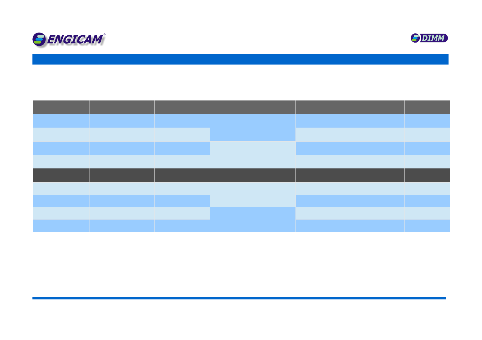
3.1 Ordering Information
n the following table some examples of orderable codes, informations and the descriptions for the modules' basic technical specifications:
Part name Ordering Code MPQ Description CPU & Memory specifications CPU junction
temperature range °C
Operating temperature
range °C (excepted CPU)
Module available at
least until 1)
GEA M6UL NAND FULL 0026820032I02C 1SOD MM Module
GEA M6UL FULL ED MM i.MX6UL MC MX6G2, 528MHz,
256MB DDR3, 256MB NAND,
Dual Ethernet, nd. Temp.
-40 to +105 -40 to +85 4 th Q - 2030
GEA M6UL NAND FULL 0026720032I02C 58 SOD MM Module
GEA M6UL FULL -40 to +105 -40 to +85 4 th Q - 2030
GEA M6UL NAND BAS C 0026800032I01C 1SOD MM Module
GEA M6UL BAS C ED MM i.MX6UL MC MX6G2, 528MHz,
128MB DDR3, 256MB NAND,
Single Ethernet, nd. Temp.
-40 to +105 -40 to +85 4 th Q - 2030
GEA M6UL NAND BAS C 0026700032I01C 58 SOD MM Module
GEA M6UL BAS C -40 to +105 -40 to +85 4 th Q - 2030
eMMC ersion Ordering Code MPQ Description CPU & Memory specifications CPU junction
temperature range °C
Operating temperature
range °C (excepted CPU)
Module available at
least until 1)
GEA M6UL eMMC BAS C 8G 0026800032I53C 1SOD MM Module
GEA M6UL eMMC BAS C ED MM i.MX6UL MC MX6G2, 528MHz,
512MB DDR3, 8GB eMMC, Single
Ethernet, ndustrial
-40 to +105 -40 to +85 4 th Q - 2030
GEA M6UL eMMC BAS C 8G 0026700032I53C 58 SOD MM Module
GEA M6UL eMMC BAS C -40 to +105 -40 to +85 4 th Q - 2030
GEA M6UL eMMC BAS C 4G 0026800032E41C 1SOD MM Module
GEA M6UL eMMC BAS C ED MM i.MX6UL MC MX6G2, 528MHz,
128MB DDR3, 4GB eMMC, Single
Ethernet, Extended temp.
-40 to +105 -25 to +85 4 th Q - 2030
GEA M6UL eMMC BAS C 4G 0026700032E41C 58 SOD MM Module
GEA M6UL eMMC BAS C -40 to +105 -25 to +85 4 th Q - 2030
Table 1
Note: See the structure in the following page for the description of ordering code nomenclature, characteristics and options.
1) Long Term Availability based on NXP longevity program
D N : 9

he module is available with both NAND and eMMC option. he main order codes, shown in the table above, could be modified
following the structure below:
0026
0026 -
-A
A-
-B
B-
-CCC
CCC -
-D
D-
-E
E-
-F
F-
-G
G-
-H
H
H
HReserved
Reserved
MPQ
MPQ A
AG
GRAM SIZE
RAM SIZE
58 7 1 128MB
1 8 2 256MB
3 512MB
OPTION A AILABLE
OPTION A AILABLE B
B
Single ethernet (BASIC) 0F
FNON OLATILE MEMORY SPECIFICATION
NON OLATILE MEMORY SPECIFICATION
Dual ethernet (FULL) 20 256MB SLC NAND
1 512MB SLC NAND
4 4GB eMMC
SOM TYPE
SOM TYPE CCC
CCC 5 8GB eMMC
GEA M6UL 003
CPU TYPE RELATED TO SOM
CPU TYPE RELATED TO SOM D
DE
ETEMPERATURE QUALIFIER
TEMPERATURE QUALIFIER
- - C -
- - E Extended Temperature
G2 2 I Industrial
- - A -
Ordering Code nomenclature
D N : 1 0

4. Pinout
This Chapter gives the pinout informations.
Section includes:
✔Pinout overview
✔i.MX Pad spacifications
✔Electrical specification
D N : 11
Chapter
4
4
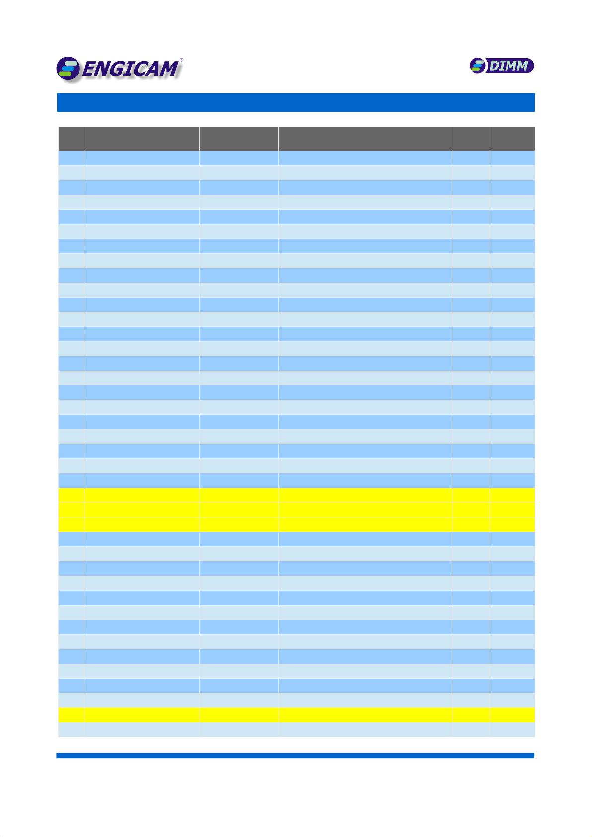
4.1 Module Pinout
The module's interface is achieved by a SO D MM 200 position connector TYCO ELECTRON CS code 1473005-1 or compatible
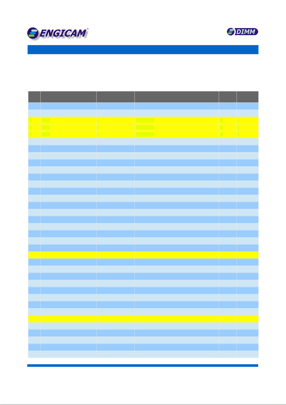
Pin Name Pin Name on I.MX6 Primary Function Description GPIO
Capable
oltage
1 +1V8 - Output Power P N - -
2 +1V8 - Output Power P N - -
3 GND - Power P N N -
4 GND - Power P N N -
5 GND - Power P N N -
6 GP O5_ O00 SNVS_TAMPER0 Spare GP O Y +3,3V
7 GP O5_ O01 SNVS_TAMPER1 Spare GP O Y +3,3V
8 GP O5_ O02 SNVS_TAMPER2 Spare GP O Y +3,3V
9 GP O5_ O03 SNVS_TAMPER3 Spare GP O Y +3,3V
10 GP O5_ O04 SNVS_TAMPER4 Spare GP O Y +3,3V
11 GP O5_ O07 SNVS_TAMPER7 Spare GP O Y +3,3V
12 GP O5_ O08 SNVS_TAMPER8 Spare GP O Y +3,3V
13 GP O5_ O09 SNVS_TAMPER9 Spare GP O Y +3,3V
14 GP O1_ O10 JTAG_MOD Spare GP O Y +3,3V
15 GP O3_23 1) LCD_DATA18 Spare GP O Y +3,3V
16 GP O3_24 3) LCD_DATA19 Spare GP O Y +3,3V
17 NC - - N -
18 +Vcoin 2) VDD_SNVS_ N Backup battery or RTC - -
19 NC - - - -
20 NC - - - -
21 NC - - - -
22 GND - Power P N N -
23 2C1_SCL UART4_TX_DATA 2C SCL Signal Y +3,3V
24 2C1_SDA UART4_RX_DATA 2C SDA Signal Y +3,3V
25 TOUCH_XP GP O1_ O04 Touch Screen Xp (touch controller input) - +3,3V
26 TOUCH_XN GP O1_ O03 Touch Screen Xn (touch controller input) - +3,3V
27 TOUCH_YP GP O1_ O02 Touch Screen Yp (touch controller input) - +3,3V
28 TOUCH_YN GP O1_ O01 Touch Screen Yn (touch controller input) - +3,3V
29 NC - - - -
30 NC - - - -
31 GND - Power P N N -
32 NC - - - -
33 ADC0_W PER GP O1_ O00 Analog nput Y +3,3V
34 AUD_MCLK JTAG_TMS 2S Master Clock Y +3,3V
35 GP O4_14 NAND_CE1_B Generic GP O Y +3,3V
36 GP O4_16 NAND_DQS Generic GP O Y +3,3V
D N : 1 2

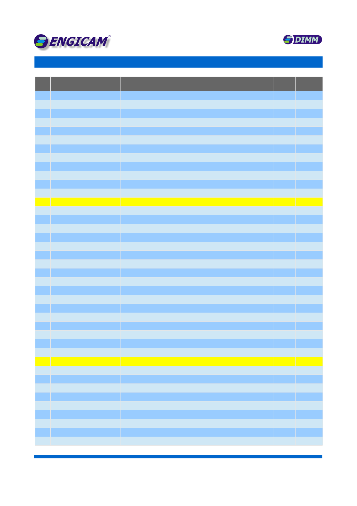
Pin Name Pin Name on I.MX6 Primary Function Description GPIO
Capable
oltage
37 SD2_CD CS _MCLK uSDHC2 CD Signal Y +3,3V
38 GP O1_8 GP O1_ O08 Generic GP O Y +3,3V
39 GND - Power P N - -
40 GP O4_18 CS _P XCLK Generic GP O Y +3,3V
41 NC - - - -
42 NC - - - -
43 NC - - - -
44 NC - - - -
45 NC - - - -
46 NC - - - -
47 NC - - - -
48 NC - - - -
49 NC - - - -
50 NC - - - -
51 NC - - - -
52 NC - - - -
53 NC - - - -
54 NC - - - -
55 NC - - - -
56 NC - - - -
57 NC - - - -
58 NC - - - -
59 NC - - - -
60 NC - - - -
61 NC - - - -
62 GP O3_4 LCD_RESET Generic GP O Y +3,3V
63 SP 1_MOS CS _DATA06 Enhanced Configurable SP MOS Y +3,3V
64 GND - Power P N N -
65 GP O3_27 1) LCD_DATA22 Generic GP O Y +3,3V
66 GP O1_25 UART3_RX_DATA Generic GP O Y +3,3V
67 NC - - - -
68 SP 1_SS0 CS _DATA05 Enhanced Configurable SP Chip Select Y +3,3V
69 NC - - - -
70 NC - - -
71 GND - Power P N N -
72 SP 1_CLK CS _DATA04 Enhanced Configurable SP CLK Y +3,3V
73 SP 1_M SO CS _DATA07 Enhanced Configurable SP M SO Y +3,3V
74 NC - - - -
75 NC - - - -
76 NC - - - -
D N : 1 3
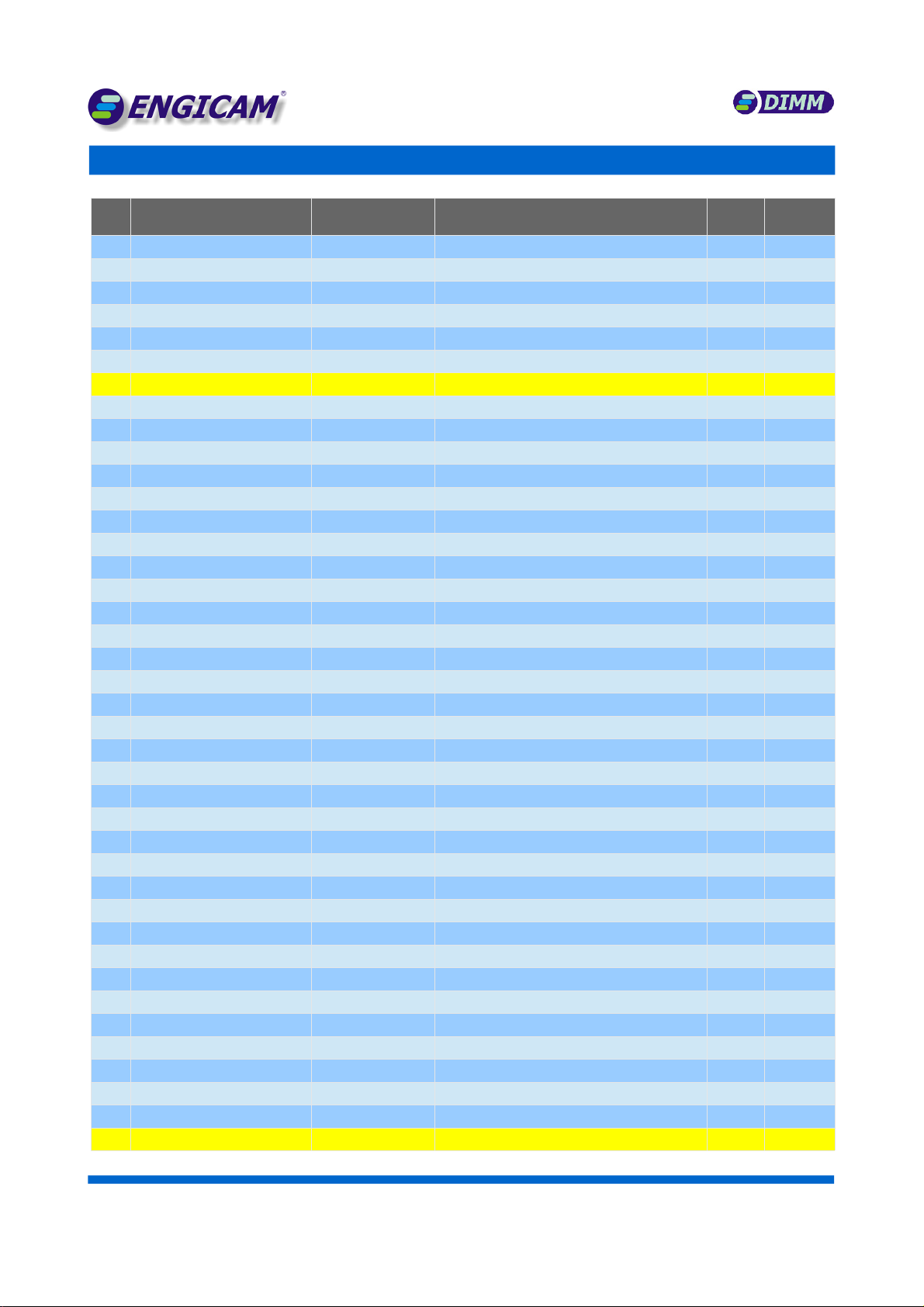
Pin Name Pin Name on I.MX6 Primary Function Description GPIO
Capable
oltage
77 NC - - - -
78 NC - - - -
79 GP O1_18 UART1_CTS_B Generic GP O - -
80 nSD_BOOT 1) - - - +3,3V
81 NC - - - -
82 NC - - - -
83 NC - - - -
84 NC - - - -
85 NC - - - -
86 NC - - - -
87 NC - - - -
88 NC - - - -
89 GND - Power P N N -
90 NC - - - -
91 NC - - - -
92 NC - - - -
93 NC - - - -
94 ETH1_TXP 4) - Fast Ethernet TXP signal - -
95 NC - - - -
96 ETH1_TXN 4) - Fast Ethernet TXN signal - -
97 ETH1_LED_10_100_KATHOD 4) - Led ndicator Cathode signal - -
98 ETH1_RXP 4) - Fast Ethernet RXP signal - -
99 ETH1_LED_ACT_ANOD 4) - Led indicator Anode signal - -
100 ETH1_RXN 4) - Fast Ethernet RXN signal - -
101 NC - - - -
102 NC - - - -
103 NC - - - -
104 NC - - - -
105 UART8_CTS ENET2_TX_CLK UART8 CTS signal Y +3,3V
106 UART8_RTS 1) LCD_DATA23 UART8 RTS signal Y +3,3V
107 GND - Power P N N -
108 UART8_TXD 3) LCD_DATA20 UART8 TXD signal Y +3,3V
109 UART8_RXD 3) LCD_DATA21 UART8 RXD signal Y +3,3V
110 2C2_SDA UART5_RXD 2C SDA Signal Y +3,3V
111 2C2_SCL UART5_TXD 2C SCL Signal Y +3,3V
112 UART2_TXD UART2_TXD UART2 TXD signal Y +3,3V
113 UART2_RXD UART2_RXD UART2 RXD signal Y +3,3V
114 2S_D N JTAG_TCK 2S Data n Y +3,3V
115 2S_LRCLK JTAG_TDO 2S RCLK Y +3,3V
116 UART1_TXD UART1_TXD UART1 TXD signal Y +3,3V
D N : 1 4
Pin Name Pin Name on I.MX6 Primary Function Description GPIO
Capable
oltage
117 UART1_RXD UART1_RXD UART1 RXD signal Y +3,3V
118 CAN1_TX UART3_CTS CAN 1 transmit signal Y +3,3V
119 CAN1_RX UART3_RTS CAN 1 receive signal Y +3,3V
120 CAN2_TX UART2_CTS CAN 2 transmit signal Y +3,3V
121 CAN2_RX UART2_RTS CAN 2 receive signal Y +3,3V
122 2S_DOUT JTAG_TRST 2S Data Out Y +3,3V
123 GND - Power P N N -
124 2S_SCLK JTAG_TD 2S SCLK Y +3,3V
125 D SP0_CLK LCD_CLK LCD interface Y +3,3V
126 NC - - - -
127 ETH0_TXN - Fast Ethernet TXN signal - -
128 nRESET POR_B Reset signal N +3,3V
129 ETH0_TXP - Fast Ethernet TXP signal - -
130 NC - - - -
131 ETH0_RXN - Fast Ethernet RXN signal - -
132 D SP0_CONTRAST ENET1_RX_ER LCD interface Y +3,3V
133 ETH0_RXP - Fast Ethernet RXP signal - -
134 +3V3_OUT - Output Power P N N -
135 +3V3_OUT - Output Power P N N -
136 NC - - - -
137 ETH0_LED_10_100_KATHOD - Led ndicator Cathode signal - -
138 NC - - - -
139 ETH0_LED_ACT_ANOD - Led indicator Anode signal - -
140 +3V3_OUT - Output Power P N - -
141 D SP0_D17 1) LCD_DATA17 LCD interface Y +3,3V
142 D SP0_D16 1) LCD_DATA16 LCD interface Y +3,3V
143 D SP0_D15 1) LCD_DATA15 LCD interface Y +3,3V
144 D SP0_D14 1) LCD_DATA14 LCD interface Y +3,3V
145 D SP0_D13 1) LCD_DATA13 LCD interface Y +3,3V
146 D SP0_D12 1) LCD_DATA12 LCD interface Y +3,3V
147 D SP0_D11 1) LCD_DATA11 LCD interface Y +3,3V
148 D SP0_D10 1) LCD_DATA10 LCD interface Y +3,3V
149 D SP0_D9 1) LCD_DATA09 LCD interface Y +3,3V
150 D SP0_D8 1) LCD_DATA08 LCD interface Y +3,3V
151 D SP0_D7 1) LCD_DATA07 LCD interface Y +3,3V
152 D SP0_D6 1) LCD_DATA06 LCD interface Y +3,3V
153 D SP0_D5 1) LCD_DATA05 LCD interface Y +3,3V
154 D SP0_D4 1) LCD_DATA04 LCD interface Y +3,3V
155 D SP0_D3 1) LCD_DATA03 LCD interface Y +3,3V
156 GND - Power P N N -
D N : 1 5
Pin Name Pin Name on I.MX6 Primary Function Description GPIO
Capable
oltage
157 D SP0_D2 1) LCD_DATA02 LCD interface Y +3,3V
158 D SP0_D1 1) LCD_DATA01 LCD interface Y +3,3V
159 D SP0_D0 1) LCD_DATA00 LCD interface Y +3,3V
160 D SP0_VSYNC LCD_VSYNC LCD interface Y +3,3V
161 D SP0_HSYNC LCD_HSYNC LCD interface Y +3,3V
162 D SP0_DRDY LCD_ENABLE LCD interface Y +3,3V
163 NC - - - -
164 NC - - - -
165 NC - - - -
166 SD2_D3 3) CS _DATA03 uSDHC2 DAT 3 signal Y +3,3V
167 SD2_CMD 3) CS _HSYNC uSDHC2 CMD signal Y +3,3V
168 SD2_D0 3) CS _DATA00 uSDHC2 DAT 0 signal Y +3,3V
169 SD2_CLK 3) CS _VSYNC uSDHC2 CLK signal Y +3,3V
170 SD2_D2 3) CS _DATA02 uSDHC2 DAT 2 signal Y +3,3V
171 SD2_D1 3) CS _DATA01 uSDHC2 DAT 1 signal Y +3,3V
172 NC - - - -
173 NC - - -
174 NC - - -
175 NC - - -
176 NC - - -
177 NC - - -
178 NC - - -
179 NC - - -
180 USB_H1_VBUS USB_OTG2_VBUS USB HOST interface N -
181 BOOT_MODE BOOT_MODE Boot from USB UART or on board Nand Flash - -
182 GND - Power P N N -
183 SD1_CD UART1_RTS_B uSDHC1 CD Signal Y +3,3V
184 GP O1_9 GP O1_ O09 Generic GP O - uSDHC1 WP Signal Y +3,3V
185 SD1_D2 SD1_DATA2 uSDHC1 DAT 2 signal Y +3,3V
186 SD1_D3 SD1_DATA3 uSDHC1 DAT 3 signal Y +3,3V
187 SD1_D1 SD1_DATA1 uSDHC1 DAT 1 signal Y +3,3V
188 SD1_D0 SD1_DATA0 uSDHC1 DAT 0 signal Y +3,3V
189 SD1_CLK SD1_CLK uSDHC1 CLK signal Y +3,3V
190 SD1_CMD SD1_CMD uSDHC1 CMD signal Y +3,3V
191 USB_OTG_ D UART3_TX_DATA USB on the go interface N -
192 USB_OTG_DP USB_OTG1_DP USB on the go interface N -
193 USB_OTG_DN USB_OTG1_DN USB on the go interface N -
194 USB_H1_DP USB_OTG2_DP USB HOST interface N -
195 USB_OTG_VBUS USB_OTG1_VBUS USB on the go interface N -
196 USB_H1_DN USB_OTG2_DN USB HOST interface N -
D N : 1 6

Pin Name Pin Name on I.MX6 Primary Function Description GPIO
Capable
oltage
197 +5Vin - Power P N N -
198 +5Vin - Power P N N -
199 +5Vin - Power P N N -
200 +5Vin - Power P N N -
Table 2
1) Note: for the use of this pin please refer to boot option in “Boot Mode Pin” chapter
2) Connect to Coin-Cell or Super-Cap; left floating if not use
3) WARNING: the peripheral SD2 (uSDHC2) is not available in the modules that mount the eMMC
4) Note: that Ethernet 1 is available only for FULL versions module
The yellow lines highlight the required minimum electrical connections in order to make the module working correctly.
4.2 What's new
Peripheral RE B RE A
Added memory device eMMC (option) Only NAND
Table 3
WARNING:
the peripheral SD2 (uSDHC2) is not available in the modules that mount the eMMC. Some peripherals, e.g. the Wi-Fi modules
that use SD interface can not be used
D N : 1 7

4.3 Electrical specifications
Min ( olts) Typ ( olts) Max ( olts)
Vin 1) + 3,6 2) + 5 + 5,5
VBUS_OTG_USB, VBUS_USB + 4,40 + 5 +5.35
GP O V(oh) + 3,15 - -
GP O V(ol) - - + 0,15
GP O V(ih) + 2,35 + 3,3
GP O V(il) 0 - + 1
Table 4
1) This measure has done testing the module's start at the limit temperatures of -40°C and +85°C
2) Warning: the use of Min voltage to power the module is not enough to power also the BUS for USB peripherals
Following, the current consumption test on module type GEA M6UL NAND BASIC, when running four different benchmarks.
Module Test condition Current @ Min Current @ Typ Current @ Max
GEA M6UL NAND BAS C
Linux Sleep mode - 15 mA -
Linux (only standard services running) - 80 mA 90 mA
QT, 2D dynamic graphic application running - 150 mA 160 mA
Table 5
The measures have been done using U-Boot revision 2.01.
D N : 1 8

5. Carrier Board Design
This Chapter gives the technical specifications for carrier board design.
Section includes:
✔Carrier Board recommendations
✔Power signals and backup battery
✔Serials
✔CAN Bus
✔Ethernet
✔USB
✔SDIO
✔LCD
✔Boot mode
✔Audio
✔Reset pin management
D N : 1 9
Chapter
5
5

5.1 Carrier board recommended specifications
Following we'll describe the specifications required to carrier board to avoid problems of assembly process. The module is interfaced
with the carrier board through a SO-D MM with 200 positions connector type TYCO ELECTRON CS code 1473005-1 or compatible.
For proper assembly is strongly recommended to paying attention to:
5.1.1 Planarity in finish process
Due to the technical and mechanical specifications of the connector we suggest the maximum planarity of the footprint on PCB, so we
suggest a type of finish obtained by horizontal process ( we suggest and use for our carrier boards a type Chemical Gold finish).
5.1.2 Planarity of PCB
Also the planarity of the entire Printed Circuit Board must be kept in check especially when the your carrier board grows in size. n this
case we suggest you contact the manufacturer of PCB to understand how improve the planarity of ended board and optimize the
process maintaining the electrical characteristics unchanged
Note: for further detail please refer to your SO-DIMM connector's data-sheet
5.1.3 Power Supply
t's strongly recommended that the power supply of the carrier board, which feeds the driver and control devices connected with the
i.MX processor, begins to work after the initialization of the processor itself
D N : 2 0
Table of contents
Other ENGICAM Carrier Board manuals


