Epson SCI 7660 SERIES User manual

1.
DC/DC Converter

SCI7660 Series
SCI7000 Series EPSON 1–1
Technical Manual
DC/DC
Converter
DESCRIPTION
The SCI7660 Series is a highly efficient CMOS DC/DC
converter for doubling an input voltage. This power-
saving IC allows portable computers and similar hand-
held equipment to operate from a single power supply,
even when they incorporate LSIs that operate at volt-
ages different from those of logic circuits, for example,
LCD drivers and analog LSIs.
The SCI7660C0B is available in 8-pin plastic DIPs, and
the SCI7660M0B, in 8-pin plastic SOPs.
FEATURES
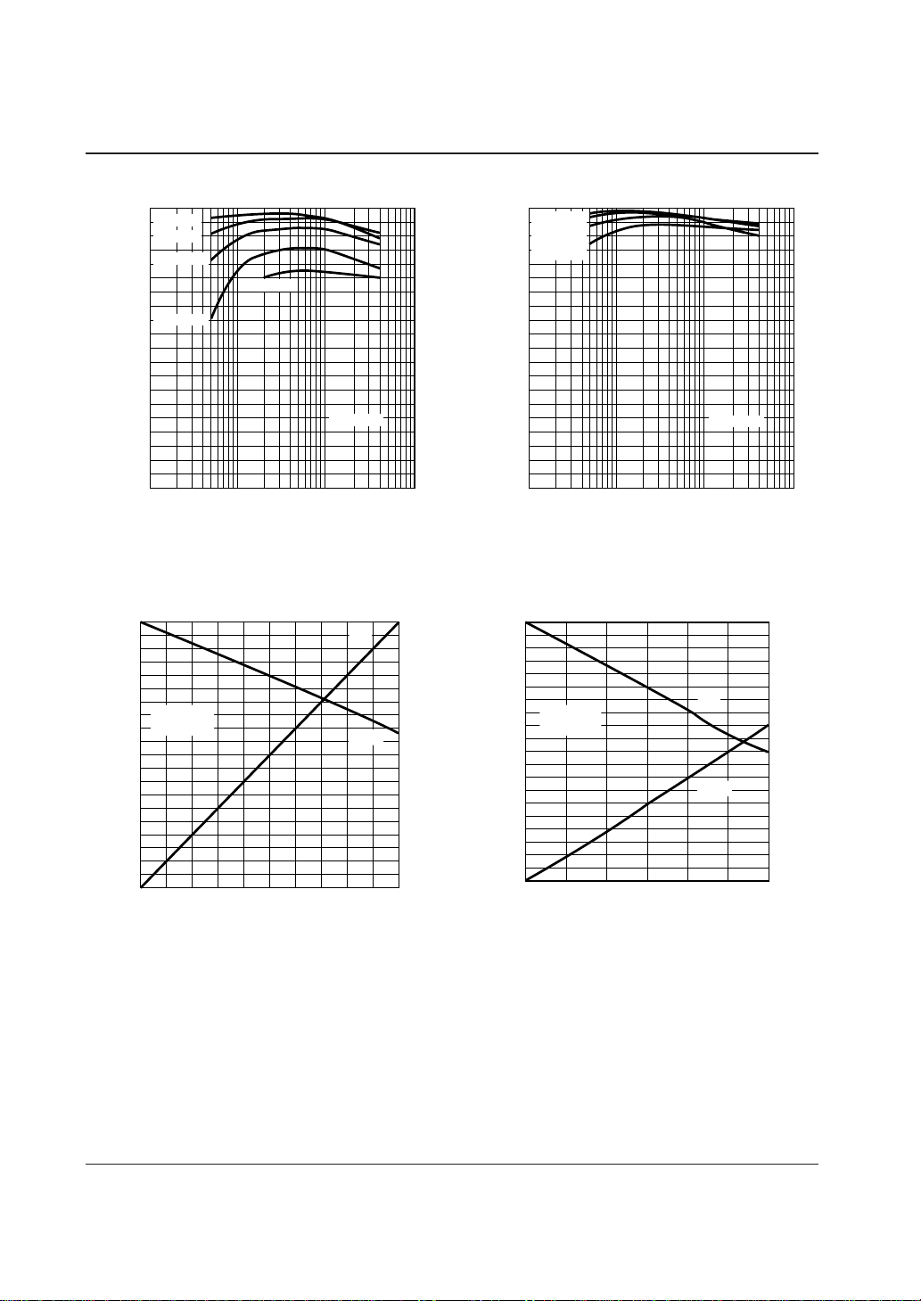
• 95% (typ.) conversion efficiency
• Two output voltages, VO, relative to VDD and VI
• 30mA maximum output current at 5V
• Two-in-series configuration doubles negative output
voltage.
• Low operating voltage
• On-chip RC oscillator
• 8-pin plastic DIP and 8-pin plastic SOP
APPLICATIONS
• Fixed-voltage power supplies for battery-operated
equipment
• Power supplies for pagers, memory cards, calculators
and similar hand-held equipment
• Fixed-voltage power supplies for medical equipment
• Fixed-voltage power supplies for communications
equipment
• Uninterruptable power supplies
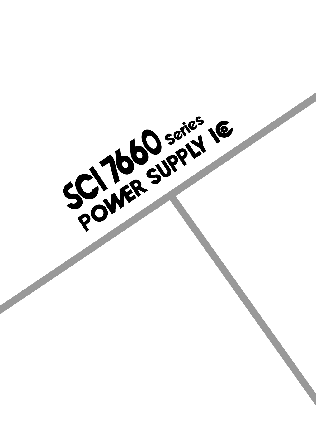
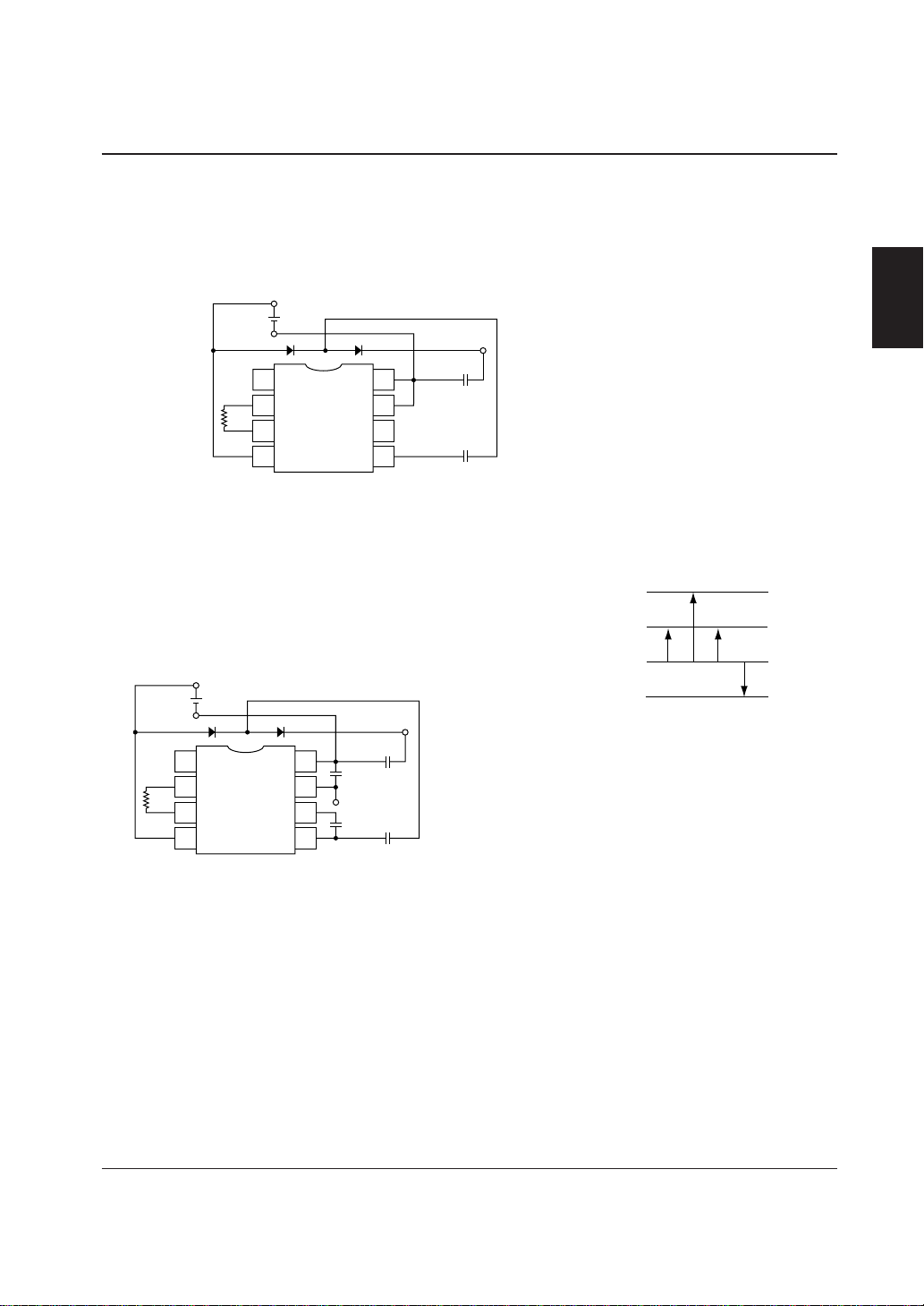
BLOCK DIAGRAM
PIN CONFIGURATION
PIN DESCRIPTION
V
DD
OSC2
V
I
CAP1–
V
O
CAP1+
Voltage converter
RC oscillator
OSC1
1
2
3
4
SCI7660C
0B
NC
OSC2
OSC1
V
DD
V
I
V
O
CAP1–
CAP1+
8
7
6
5
Number Name Description
1 NC No connection
2 OSC2 Resistor connection. Open when using external clock
3 OSC1 Resistor connection. Clock input when using external clock
4VDD Positive supply (system VCC)
5 CAP1+ Positive charge-pump connection
6 CAP1– Negative charge-pump connection
7VO×2 multiplier output
8VINegative supply (system ground)

SCI7660 Series
1–2 EPSON SCI7000 Series
Technical Manual
Parameter Symbol Rating Unit
Input voltage range VI–10.0 to 0.5 V
Output voltage range VOMin. –20.0 V
Power dissipation PD300 (DIP) mW
150 (SOP)
Operating temperature range Topr –40 to 85 ˚C
Storage temperature range
Tstg –65 to 150 ˚C
Soldering temperature(for 10s). See note.
Tsol 260 ˚C
SPECIFICATIONS
Absolute Maximum Ratings
Note:
Temperatures during reflow soldering must remain within the limits set out in LSI Device Precautions.
Never use solder dip to mount SCI7000 series power supply devices.
Recommended Operating Conditions
VDD = 0V, Ta = –40 to 85˚C unless otherwise noted
Parameter Symbol Condition Rating Unit
Min. Typ. Max.
ROSC = 1MΩ,
C1/C2≤1/20, C2≥10µF, — — –1.5
Oscillator startup voltage VSTA Ta = –40 to 85˚C V
See note 1.
ROSC = 1MΩ— — –2.2
Oscillator shutdown voltage
VSTP ROSC = 1MΩ–1.5 — — V
Load resistance RLRLmin ——Ω
See note 2.
Output current IO— — 30.0 mA
Clock frequency fOSC 10.0 — 30.0 kHz
RC oscillator network ROSC 680 — 2,000 kΩ
resistance
Capacitance C1, C23.3 — — µF
Notes:
1. The recommended circuit configuration for low-voltage operation (when VIis between –1.2V and
–2.2V) is shown in the following figure. Note that diode D1 should have a maximum forward voltage of
0.6V with 1.0mA forward current.
2. RLmin can be varied depending on the input voltage.

SCI7660 Series
SCI7000 Series EPSON 1–3
Technical Manual
DC/DC
Converter
VDD = 0V, Ta = –40 to 85˚C unless otherwise noted
Parameter Symbol Condition Rating Unit
Min. Typ. Max.
Input voltage VI–8.0 — –1.5 V
Output voltage VO–16.0 — — V
Multiplier current Iopr RL= ∞, ROSC = 1MΩ—2030µA
VI= –5V
Quiescent current IQRL=∞, VI= –8V — — 2.0 µA
Clock frequency fOSC
ROSC = 1MΩ, VI= –5V
16 20 24 kHz
Output impedance ROIO= 10mA, VI = –5V — 75 100 Ω
Multiplication efficiency Peff IO= 5mA, VI= –5V 90 95 — %
OSC1 Input leakage current
ILKI VI= –8V — — 2.0 µA
3. RLmin is a function of VI.
Electrical Characteristics
Battery C
L
D1
C2
22µF
C1
10µF
R
L
1MΩ
+
+
8
7
6
5
1
2
3
4
1.0
5
4
3
2
1
01.5 2.0
Input voltage (V)
Minimum load resistance (kΩ)
3.0
V
STA2
V
STA1
4.0 5.0 6.0

SCI7660 Series
1–4 EPSON SCI7000 Series
Technical Manual
Typical Performance Characteristics
1000
100
10
110 100 1000 10000
f
OSC
[KHz]
R
OSC
[kΩ]
V
I
= –5V
V
I
= –3V
V
I
= –2V
Ta = 25°C
26
25
24
23
22
21
20
19
18
17
16
15
14
13
12
11
10
9
8–40 –20 0 20 40
Ta [°C]
f
OSC
[KHz]
60 80 100
V
I
= –5.0V
V
I
= –3.0V
V
I
= –2.0V
Clock frequency vs. External resistance Clock frequency vs. Ambient temperature
50
45
40
35
30
25
20
15
10
5
0–7 –6 –5 –4 –3 –2 –1 0
@lopr
[µA]
V
I
[V]
Ta = 25°C
f
OSC
= 40kHz
f
OSC
=
20kHz
f
OSC
=
10kHz
0
–5
–10
–15 0 1020304050
V
O
[V]
I
O
[mA]
Ta = 25
V
I
= –5.0V
Multiplier current vs. Input voltage Output voltage vs. Output current

SCI7660 Series
SCI7000 Series EPSON 1–5
Technical Manual
DC/DC
Converter
0
–5
–10 0102030
V
O
[V]
I
O
[mA]
Ta = 25°C
V
I
= –3.0V
0
–1
–2
–3
–4
–5
–60 23456789101
V
O
[V]
I
O
[mA]
Ta = 25°C
V
I
= –2.0V
Output voltage vs. Output current Output voltage vs. Output current
300
200
100
0–7 –6 –5 –4 –3 –2 –1 0
RO[Ω]
VI[V]
Ta = 25°C
IO= 7mA
300
200
100
0–7 –6 –5 –4 –3 –2 –1 0
R
O
[Ω]
V
I
[V]
Ta = 25°C
I
o
= 10mA
Output impedance vs. Input voltage Output impedance vs. Input voltage

SCI7660 Series
1–6 EPSON SCI7000 Series
Technical Manual
100
90
80
70
60
50
40
30
20
10
01 10 100 1000
Peff [%]
f
OSC
[kHz]
I
O
= 2mA
I
O
= 5mA
I
O
= 10mA
I
O
= 20mA
I
O
= 30mA
V
I
= –5.0V
100
90
80
70
60
50
40
30
20
10
01 10 100 1000
Peff [%]
fOSC [kHz]
IO= 0.5mA
IO= 1.0mA
IO= 2.0mA
IO= 4.0mA
VI= –3.0V
Multiplication efficiency vs. Clock frequency Multiplication efficiency vs. Clock frequency
100
90
80
70
60
50
40
30
20
10
0
100
90
80
70
60
50
40
30
20
10
0
010 20 30 40 50
Peff [%]
I
I
[mA]
I
O
[mA]
Ta = 25°C
V
I
= –5.0V
I
I
Peff
100
90
80
70
60
50
40
30
20
10
0
100
90
80
70
60
50
40
30
20
10
0
0 5 10 15 20 25 30
Peff [%]
I
I
[mA]
I
O
[mA]
Ta = 25°C
V
I
= –3.0V
I
I
Peff
Multiplication efficiency/input current vs. Multiplication efficiency/input current vs.
Output current Output current

SCI7660 Series
SCI7000 Series EPSON 1–7
Technical Manual
DC/DC
Converter
FUNCTIONAL DESCRIPTION
RC Oscillator
The on-chip RC oscillator network frequency is deter-
mined by the external resistor, ROSC, connected be-
tween OSC1 and OSC2. This oscillator can be disabled
in favor of an external clock by leaving OSC2 open and
applying an external clock signal to OSC1.
OSC1
Oscillator External clock
R
OSC
OSC2
OSC1
OSC2
External clock
signal
100
90
80
70
60
50
40
30
20
10
0
40
36
32
28
24
20
16
12
8
4
0
012345678910
Peff [%]
II[mA]
IO[mA]
Ta = 25°C
VI= –2.0V
II
Peff
Multiplication efficiency/input current vs.
Output current
Voltage Multiplier
The voltage multiplier uses the clock signal from the
oscillator to double the input voltage. This requires two
external capacitors—a charge-pump capacitor, C1, be-
tween CAP1+ and CAP1–, and a smoothing capacitor,
C2, between VIand VO.
5 V
C1
10µF
C2
10µF
V
O1
= –10V (2V
I
)
V
DD
= 0 V
V
I
= –5 V
1MΩ
+
+
8
7
6
5
1
2
3
4
Doubled potential levels
V
CC
(+5V)
(–5V)
GND
V
O
= (2V
I
)
= –10 V
V
I
= –5 V
V
DD
= 0 V

SCI7660 Series
1–8 EPSON SCI7000 Series
Technical Manual
TYPICAL APPLICATIONS
Parallel Connection
Connecting two or more chips in parallel reduces the
output impedance by 1/n, where nis the number of de-
vices used.
5 V
C1
10µF
C2
10µF
V
DD
= 0 V
V
I
= –5 V
V
O
= –10 V
1MΩ
+
+
8
7
6
5
1
2
3
4
C1
10µF
1MΩ
+
8
7
6
5
1
2
3
4
Serial Connection
Connecting two or more chips in series obtains a higher
output voltage than can be obtained using a parallel connection, however, this also raises the output imped-
ance.
Potential levels
5 V
C1
10µF
C2
10µF
V
DD
= 0 V
V
I
= –5 V
V
O
' = –15 V
V
O
= –10 V = V
I
'
V
DD
' = V
I
= –5
1MΩ
+
+
8
7
6
5
1
2
3
4
C1
10µF
C2
10µF
1MΩ
+
+
8
7
6
5
1
2
3
4
V
DD
(0 V)
V
I
(–5 V)
V
O
(–10 V)
Primary stage Secondary stage
V
DD
V
I
V
O
(–15 V)

SCI7660 Series
SCI7000 Series EPSON 1–9
Technical Manual
DC/DC
Converter
Positive Voltage Conversion
Diodes can be added to a circuit connected in parallel to
make a negative voltage positive.
5 V
C2
10µF
V
DD
= 0 V
V
O
' = 3.8 V
V
I
= –5 V
1MΩ
+
C1
10µF
+
8
7
6
5
1
2
3
4
Simultaneous Voltage Conversion
Combining a multiplier circuit with a positive voltage
conversion circuit generates both –10 and 3.8 V outputs
from a single input.
Potential levels
5 V
C2
10µF
VDD = 0 V
VO2 = 3.8 V
VO1 = –10 V
VI= –5 V
1MΩ
++
C3
C4
10µF
10µF
+
8
7
6
5
1
2
3
4C1
10µF
+
VO2 = 3.8 V
VO1 = –10 V
VDD = 0 V
VI= –5 V
Table of contents
Other Epson Power Supply manuals
Popular Power Supply manuals by other brands

EMC2
EMC2 302-000-589 Disassembly instructions

Elektro-Automatik
Elektro-Automatik EA-PS 9080-100 manual

WAGO
WAGO 2787-2147/0000-00 0 Series manual

Alpha Technologies
Alpha Technologies Alpha Outback Energy AlphaCap-665 Installation & operation manual

Bluetti
Bluetti AC180 user manual

CAME
CAME VA/200.01 manual