Epson SCI 7661 Series User manual

2.
DC/DC Converter
& Voltage Regulator

SCI7661 Series
SCI7000 Series EPSON 2–1
Technical Manual
DC/DC Converter
& Voltage Regulator
DESCRIPTION
The SCI7661 Series is a highly effecient CMOS DC/
DC converter for doubling or tripling an input voltage.
It incorporates an on-chip voltage regulator to ensure
stable output at the specified voltage. The SCI7661 Se-
ries offers a choice of three, optional temperature gradi-
ents for applications such as LCD panel power supplies.
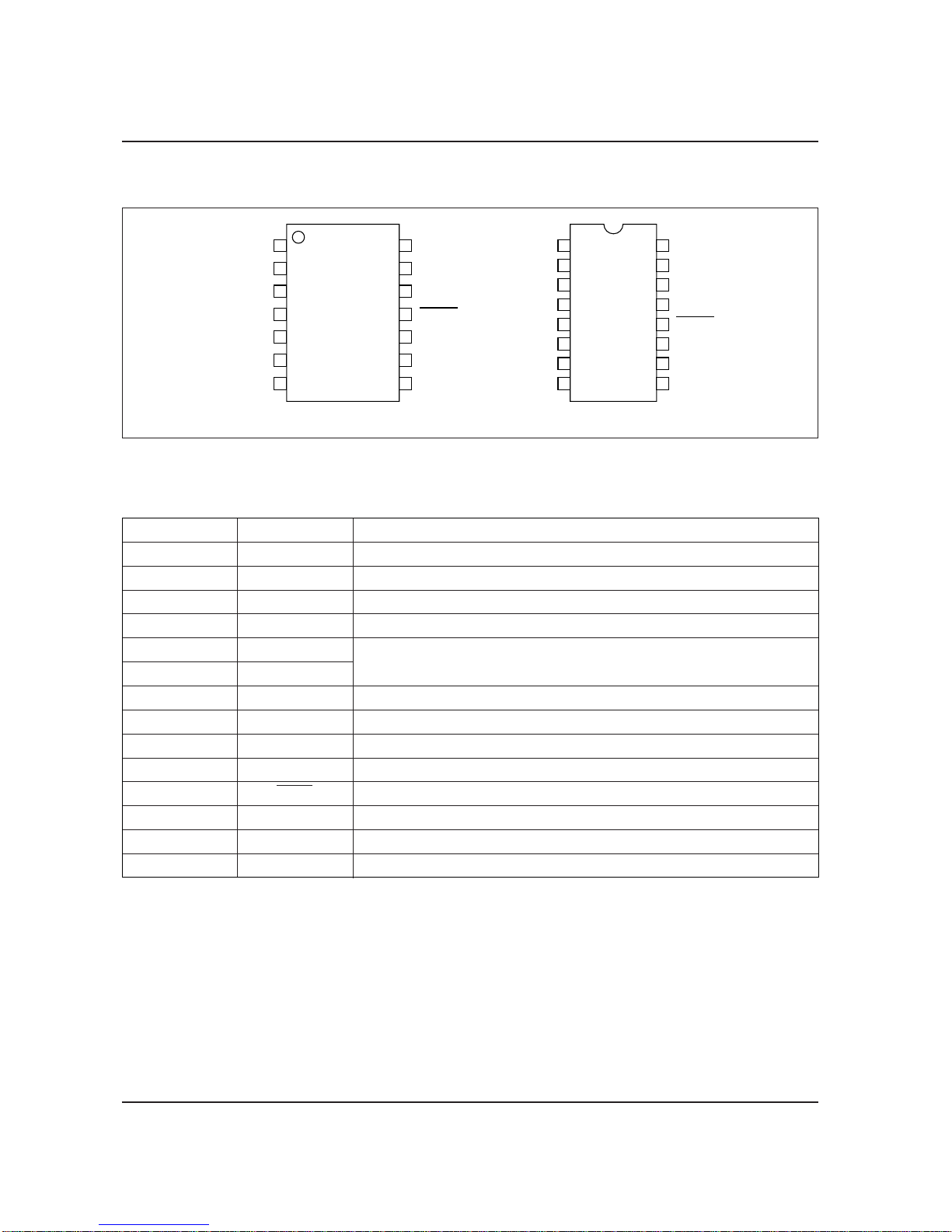
The SCI7661C0B is available in 14-pin plastic DIPs, the
SCI7661M0B, in 14-pin plastic SOPs, and the
SCI7661MBB in 16-pin plastic SSOPs.
FEATURES
• 95% (Typ.) conversion efficiency
• Up to four output voltages, VO, relative to the input
voltage, VI
• On-chip voltage regulator
• 20mA maximum output current at VI= –5V
• Three temperature gradients––0.1, 0.4 and 0.6%/°C
• External shut-down control
•2µA maximum output current when shut-down
• Two-in-series configuration doubles negative output
voltage.
• On-chip RC oscillator
• SCI7661C0B ................pladtic DIP-14 pin
SCI7661M0B...............pladtic SOP5-14 Pin
SCI7661MBB ..............pladtic SSOP2-16 pin
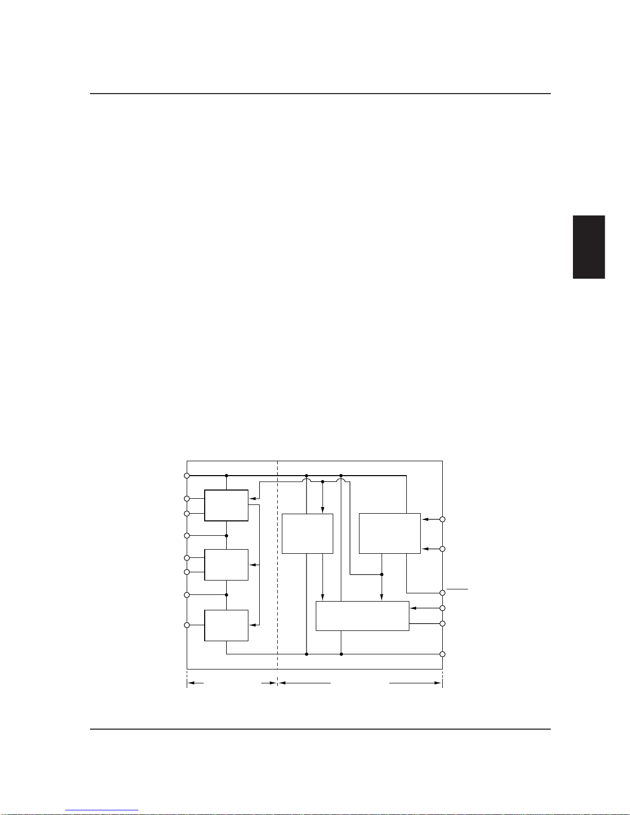
VDD
Voltage
multiplier
(1)
Voltage
multiplier
(2)
Oscilator
Reference
voltge
generator
Temperature
gradient
selector
Voltage regulator
TC1
TC2
RV
POFF
VREG
VO
VI
OSC2
OSC1
CAP1+
CAP1–
CAP2+
CAP2–
Multiplication
stage Stabilization
stage
BLOCK DIAGRAM
APPLICATIONS
• Power supplies for LCD panels
• Fixed-voltage power supplies for battery-operated
equipment
• Power supplies for pagers, memory cards, calculators
and similar hand-held equipment
• Fixed-voltage power supplies for medical equipment
• Fixed-voltage power supplies for communications
equipment
• Power supplies for microcomputers
• Uninterruptable power supplies

SCI7661 Series
2–2 EPSON SCI7000 Series
Technical Manual
PIN CONFIGURATION
PIN DESCRIPTION
1
2
3
4
5
6
7
8
1
2
3
4
5
6
7
CAP+
CAP–
CAP2+
CAP2–
TC1
TC2
V
I
14
13
12
11
10
9
8
V
DD
OSC1
OSC2
POFF
RV
V
REG
V
O
CAP+
CAP–
NC
CAP2+
CAP2–
TC1
TC2
V
I
V
DD
OSC1
NC
OSC2
POFF
RV
V
REG
V
O
16
15
14
13
12
11
10
9
SCI7661M
BB
SCI7661C
0B
/M
0B
Description
Positive charge-pump connection for ×2 multiplier
Negative charge-pump connection for ×2 multiplier
Positive charge-pump connection for ×3 multiplier
Negative charge-pump connection for ×3 multiplier or ×2 multiplier output
Number
1
2
3
4
5
6
7
8
9
10
11
12
13
14
Name
CAP1+
CAP1–
CAP2+
CAP2–
TC1
TC2
VI
VO
VREG
RV
POFF
OSC2
OSC1
VDD
Temperature gradient selects
Negative supply (system ground)
×3 multiplier output
Voltage regulator output
Voltage regulator output adjust
Voltage regulator output ON/OFF control
Resistor connection. Open when using external clock
Resistor connection. Clock input when using external clock
Positive supply (system VCC)

SCI7661 Series
SCI7000 Series EPSON 2–3
Technical Manual
DC/DC Converter
& Voltage Regulator
SPECIFICATIONS
Absolute Maximum Ratings
Notes
1. Using the IC under conditions exceeding the aforementioned absolute maximum ratings may lead to permanent destruction of
the IC. Also, if an IC is operated at the absolute maximum ratings for a longer period of time, its functional reliability may be
substantially deteriorated.
2. All the voltage ratings are based on VDD = 0V.
3. The output terminals (VO,VREG) are meant to output boosted voltage or stabilized boosted voltage. They, therefore, are not the
terminals to apply an external voltage. In case the using specifications unavoidably call for application of an external voltage,
keep such voltage below the voltage ratings given above.
Reconmmended Operating Conditions
VDD = 0V, Ta = –40 to 85˚C unless otherwise noted
Notes
1. The recommended circuit configuration for low-valtage operation (when VIis between –1.2V and –2.2V) is shown in
the following figure. Note that diode D1 should have a maximum forward voltage of 0.6V with 1.0mA forward current.
2. RLmin can be varied depending on the input voltage.
N = 2: Boosting to a double voltage
N = 3: Boosting to a triple voltage
OSC1, OSC2, POFF
TC1, TC2, RV
VONote 3)
VREG Note 3)
Plastic package
Items Codes Ratings Units Remarks
Input supply voltage
Input terminal voltage
Output voltage
Allowable dissipation
Working temperature
Storage temperature
Soldering temperature
and time
VI– VDD
VI– VDD
VO– VDD
Pd
Topr
Tstg
Tsol
–20/N to VDD + 0.3
VI– 0.3 to VDD + 0.3
VO– 0.3 to VDD + 0.3
–20 to VDD + 0.3
VOto VDD + 0.3
Max. 300
–40 to 85
–55 to 150
260°C
10 s (at leads)
V
V
V
V
V
mW
°C
°C
–
Rating
Parameter Symbol Conditions
Oscillator startup voltage
Oscillator shutdown voltage
Load resistance
Output current
Clock frequency
RC oscillator network resistance
Capacitance
Stabilization voltage sensing resis-
tance
VSTA
VSTP
RL
IO
fOSC
ROSC
C1, C2, C3
RRV
ROSC =1MΩ
C3= 10 µF, CL/C3≤1/20,
Ta = –40 to 85˚C.
See note 1.
ROSC = 1MΩ
ROSC = 1MΩ
Min.
–
–
–1.8
RLmin.
See note 2.
–
10.0
680
3.3
100
Typ.
–
–
–
–
–
–
–
–
–
Max.
–1.8
–2.2
–
–
20.0
30.0
2,000
–
1,000
Unit
V
V
Ω
mA
kHz
kΩ
µF
kΩ

SCI7661 Series
2–4 EPSON SCI7000 Series
Technical Manual
3. RLmin is a function of V1
Electrical Characteristics
VDD = 0V, V1= –5V, Ta = –40 to 85°C unless otherwise noted
C1
10µF
C2
10µF
1
2
3
4
5
6
7
14
13
12
11
10
9
8
R
OSC
C
L
R
L
1MΩ
C3
22µF
D1
+
+
+
5
4
3
2
1
01Input voltage (V)
Minimum load resistance (kΩ)
654321.5
V
STA2
V
STA1
Voltage
tripler
Voltage
doubler
SymbolParameter Conditions
Input voltage
Output voltage
Regulator voltage
Stabilization circuit operating voltage
Multiplier current
Stabilization current
Quiescent current
Clock frequency
VI
VO
VREG
VO
Iopr1
Iopr2
IQ
fOSC
RL= ∞, RRV = 1MΩ,
VO= –18V
RL= ∞, ROSC = 1MΩ
RL= ∞, RRV = 1MΩ,
VO= –15V
TC2 = TC1 = VO, RL= ∞
ROSC = 1MΩ
Rating
Min.
–6.0
–18.0
–18.0
–18.0
–
–
–
16.0
Typ.
–
–
–
–
40
5.0
–
20.0
Max.
–1.8
–
–2.6
–3.2
80
12.0
2.0
24.0
Unit
V
V
V
V
µA
µA
µA
kHz

SCI7661 Series
SCI7000 Series EPSON 2–5
Technical Manual
DC/DC Converter
& Voltage Regulator
Unit
Ω
%
%/V
Ω
Ω
V
%/˚C
µA
Parameter
Output impedance
Multiplication efficiency
Stabilization output voltage
differential
Stabilization output load differential
Stabilization output saturation
resistance
Reference voltage
Temperature gradient
POFF, TC1, TC2, OSC1, and RV
input leakage current
Symbol
RO
Peff
RSAT
VRV
CT
ILKI
∆VREG
∆IO
Conditions
IO= 10mA
IO= 5mA
∆VREG
∆VO·VREG
VO= –18 to –8V,
VREG = –8V, RL= ∞,
Ta = 25˚C
VO= –15V,
VREG = –8V, Ta = 25˚C,
IO= 0 to 10µA,
TC1 = VDD, TC2 = VO
RSAT = ∆(VREG – VO)/∆IO,
IO= 0 to 10µA,
RV= VDD, Ta = 25˚C
TC2 = TC1 = VO,
Ta = 25˚C
TC2 = VDD, TC1 = VO,
Ta = 25˚C
See note.
Rating
Min.
–
90.0
–
–
–
–2.3
–1.7
–1.1
–0.25
–0.5
–0.7
–
Typ.
150
95.0
0.2
5.0
8.0
–1.5
–1.3
–0.9
–0.1
–0.4
–0.6
–
Max.
200
–
–
–
–
–1.0
–1.1
–0.8
–0.01
–0.3
–0.5
2.0
RC2 = VO, TC1 = VDD,
Ta = 25˚C
Note
|VREG (50°C)| – |VREG (0°C)|
50°C – 0°C100
|VREG (25°C)|
CT= ×

SCI7661 Series
2–6 EPSON SCI7000 Series
Technical Manual
Typical Performance Characteristics
1000
100
10
110 100 1000 10000
R
OSC
[kΩ]
f
OSC
[kHz]
VI= –5V
VI= –3V
VI= –2V
Ta = 25°C
26
25
24
23
22
21
20
19
18
17
16
15
14
13
12
11
10
9
8–40 –20 0 20 40 60 80 100
Ta [°C]
fOSC [KHz]
VI= –5.0V
VI= –3.0V
VI= –2.0V
Clock frequency vs. External resistance Clock frequency vs. Ambient temperature
150
100
50
0–7 –6 –5 –4 –3 –2 –1 0
V
I
[V]
Iopr [µA]
f
OSC
= 40kHz
f
OSC
=
20kHz
f
OSC
= 10kHz
Ta = 25°C
0
–5
–10
–150 10203040
I
O
[mA]
V
O
[V]
Ta = 25°C
V
I
= –5.0V
×2 multiplier
×3 multiplier
Multiplier current vs. Input voltage Output voltage vs. Output current

SCI7661 Series
SCI7000 Series EPSON 2–7
Technical Manual
DC/DC Converter
& Voltage Regulator
0
–5
–10
–15 0 102030
IO[mA]
Vo [V]
×2 multiplier
×3 multiplier
Ta = 25°C
VI= –3.0V
IO[mA]
VO[V]
0
012345678910
–1
–2
–3
–4
–5
–6
Ta = 25°C
VI= –2.0V
×2 multiplier
×3 multiplier
Output voltage vs. Output current Output voltage vs. Output current
100
90
80
70
60
50
40
30
20
10
0
100
90
80
70
60
50
40
30
20
10
0
0 1020304050
I
O
[mA]
I
I
[mA]
Peff [%]
×3 multiplier
I
I
Ta = 25°C
V
I
= –5.0V
×2 multiplier
Peff
×3 multiplier
Peff
×2 multiplier
I
I
0 5 10 15 20 25 30
I
O
[mA]
60
54
48
42
36
30
24
18
12
6
0
I
I
[mA]
100
90
80
70
60
50
40
30
20
10
0
Peff [%]
Ta = 25°C
V
I
= –3.0V
×3 multiplier
I
I
×3 multiplier
Peff
×2 multiplier
Peff
×2 multiplier
I
I
Multiplication efficiency/input current vs. Multiplication efficiency/input current vs.
Output current Output current

SCI7661 Series
2–8 EPSON SCI7000 Series
Technical Manual
012345678910
I
O
[mA]
I
I
[mA]
100
90
80
70
60
50
40
30
20
10
0
40
36
32
28
24
20
16
12
8
4
0
Peff [%]
Ta = 25°C
V
I
= –2.0V
×2 multiplier
Peff
×3 multiplier
Peff
×3 multiplier
I
I
×2 multiplier
I
I
500
400
300
200
100
0–7 –6 –5 –4 –3 –2 –1 0
V
I
[V]
Rout [Ω]
Ta = 25°C
I
O
= 6mA
×3 multiplier
×2 multiplier
Multiplication efficiency/input current vs. Output impedance vs. Input voltage
Output current
–7 –6 –5 –4 –3 –2 –1 0
V
I
[V]
500
400
300
200
100
0
Rout [Ω]
×3 multiplier
Ta = 25°C
I
O
= 10mA
×2 multiplier
100
90
80
70
60
50 1 10 100 1000
fOSC [kHz]
Peff [%]
IO= 2mA
IO= 5mA
IO= 10mA
IO= 20mA
IO= 30mA Ta = 25°C
VI= –5.0V
Output impedance vs. Input voltage Multiplication efficiency vs. Clock frequency

SCI7661 Series
SCI7000 Series EPSON 2–9
Technical Manual
DC/DC Converter
& Voltage Regulator
1 10 100 1000
f
OSC
[kHz]
100
90
80
70
60
50
Peff [%]
I
O
= 0.5mA
I
O
= 1.0mA
I
O
= 2.0mA
I
O
= 4.0mA
Ta = 25°C
V
I
= – 3.0V
VO= –15V
–7.850
–7.900
–7.950
–8.000
0.0001 0.0010 0.0100 0.1000
Ta = 25°C
VREG [V]
IO[V]
Multiplication efficiency vs. Clock frequency Output voltage vs. Output current
–5.850
–5.900
–5.950
–6.000
0.0001 0.0010 0.0100 0.1000
VREG [V]
IO[V]
VO= –9V
Ta = 25°C
–2.850
–2.900
–2.950
–3.000
VREG [V]
0.0001 0.0010 0.0100 0.1000
IO[V]
VO= –6V
Ta = 25°C
Output voltage vs. Output current Output voltage vs. Output current

SCI7661 Series
2–10 EPSON SCI7000 Series
Technical Manual
0 5 10 15 20
0.30
0.25
0.20
0.15
0.10
0.05
0.00
Ta = 25°C
V
O
= –5V
V
O
= –10V
V
O
= –15V
I
O
[mA]
|V
REG
-V
O
| [V]
50
0
–50 –40 –20 0 20 40 60 80 100
CT0
Ta [°C]
100×|VREG(°C)|-|VREG(25°C)|/|VREG(25°C)| [%]
CT1
CT2
Regulator voltage vs. Output current Regulator output stability ratio vs.
Ambient temperature
Temperature Gradient Control
The SCI7661C0B offers a choice of three temperature
gradients which can be used to adjust the voltage regu-
lator output in applications such as power supplies for
driving LCDs.
Notes
1. The definition of LOW for POFF differs from that for TC1 and TC2.
2. The temperature gradient affects the voltage between VDD and VREG.
POFF
1 (VDD)
1
1
1
0 (V1)
0
0
0
TC2
See note 1.
LOW (VO)
LOW
HIGH (VDD)
HIGH
LOW
LOW
HIGH
HIGH
TC1
LOW (VO)
HIGH (VDD)
LOW
HIGH
LOW
HIGH
LOW
HIGH
–0.4
–0.1
–0.6
–0.6
–
–
–
–
Temperature
gradient
(%/˚C)
See note 2.
Voltage
regulator
output RC osciliator Remarks
ON
ON
ON
ON
OFF
(high impedance)
OFF
(high impedance)
OFF
(high impedance)
OFF
(high impedance)
ON
ON
ON
OFF
OFF
OFF
OFF
OFF
Serial connection
Multiplier
operational

SCI7661 Series
SCI7000 Series EPSON 2–11
Technical Manual
DC/DC Converter
& Voltage Regulator
FUNCTIONAL DESCRIPTION
Oscillator
The on-chip RC oscillator network frequency is deter-
mined by the external resistor, ROSC, connected be-
tween OSC1 and OSC2. This oscillator can be disabled
in favor of an external clock by leaving OSC2 open and
applying an external clock signal to OSC1.
OSC1
Oscillator External clock
External clock
signal
R
OSC
OSC2
OSC1
OSC2
Reference Volatge Generator and Voltage
Regulator
The reference voltage generator supplies a reference
voltage to the voltage regulator to control the output.
This voltage can be switched ON and OFF.
V
DD
V
REG
R
RV
= 100 kΩto 1 MΩ
RV
POFF Control signal
Voltage Multiplier
The voltage multiplier uses the clock signal from the
oscillator to double or triple the input voltage. This re-
quires three external capacitors–two charge-pump ca-
pacitors between CAP1+ and CAP1– and CAP2+ and
CAP2–, respectively, and a smoothing capacitor be-
tween VIand VO.
C4
R1
R2
+
10 µF
V
REG
= –8 V
V
I
= –5 V
R
RV
100 kΩ
to
1 MΩ
R
OSC
1 MΩ
C1 +
10 µF
C2
5 V +
10 µF
C3
+10 µF
V
O
= –15 V
V
DD
= 0 V
14
13
12
11
10
9
8
1
2
3
4
5
6
7
Double voltage potential levels
V
CC
(+5V)
GND
(–5V)
V
DD
= 0 V
V
I
= –5 V
V
CAP2
– = 2V
I
= –10 V
Tripled voltage potential levels
V
DD
= 0 V
V
I
= –5 V
V
O
= 3V
I
= –15 V

SCI7661 Series
2–12 EPSON SCI7000 Series
Technical Manual
TYPICAL APPLICATIONS
Voltage Tripler with Regulator
The following figure shows the circuit required to triple
the input voltage, regulate the result and add a tempera-
ture gradient of –0.4%/°C. Note that the high input im-
pedance of RV requires appropriate noise countermea-
sures.
C4
R1
R2
+
10 µF
V
REG
= –8 V
=V
RV
V
I
= –5 V
R
RV
100 kΩ
to
1 MΩ
R
OSC
1 MΩ
C1 +
10 µF
C2
5 V +
10 µF
C3
+10 µF
V
O
= –15 V
V
DD
= 0 V
14
13
12
11
10
9
8
1
2
3
4
5
6
7R
RV
R
1
Converting a Voltage Tripler to a Voltage
Doubler
To convert this curcuit to a voltage doubler, remove ca-
pacitor C2 and short circuit CAP2– to VO.
VI= –5 V
ROSC
1 MΩ
C1 +
10µF
C2
5 V +
10µF
C3
+10 µF
VO= –15 V
VDD = 0 V
14
13
12
11
10
9
8
1
2
3
4
5
6
7
Parallel Connection
Connecting two or more chips in parallel reduces the
output impedance by 1/n, where nis the number of de-
vices used.
Only the single output smoothing capacitor, C3, is re-
V
DD
= 0 V
V
I
= –5 V V
O
= –15 V V
REG
= –10 V
5 V
C1
10 µFR
OSC
1 MΩR
OSC
1 MΩ
+
C2
10 µF+
C1
10 µF+
C2
10 µF+
C4
10 µF
R
RV
100 kΩ
to
1 MΩ
+
C3
10 µF
+
1
2
3
4
5
6
7
14
13
12
11
10
9
8
1
2
3
4
5
6
7
14
13
12
11
10
9
8
quired when any number of devices are connected in
parallel. Also, the voltage regulator in one chip is suffi-
cient to regulate the combined output.

SCI7661 Series
SCI7000 Series EPSON 2–13
Technical Manual
DC/DC Converter
& Voltage Regulator
Serial Connection
Connecting two or more chips in series obtains a higher
output voltage than can be obtained using a parallel
<Precautions when connecting loads>
In case of series connections, when connecting loads
between the first stage VDD (or other potential of the
second stage VDD or up) and the second stage VREG as
shown in Fig. 2-13, be cautions about the following
point.
* When normal output is not occurring at the VREG ter-
minal such as at times of starting up or when turning
the VREG off by Poff signals, if current flows into the
second stage VREG terminal through the load from
connection, however, this also raises the output imped-
ance.
the first stage VDD (or other potential of the second
stage VDD or up) to cause a voltage exceeding the
absolute maximum rating for the second stage VDD at
the VREG terminal, normal operation of the IC may be
hampered. Consequently, When making a series
connection, insert a diode D1 between the second
stage VIand VREG as shown in Fig. 2-13 so that a
voltage exceeding the second stage VDD or up may
not be applied to the VREG terminal.
Positive Voltage Conversion
Adding diodes converts a negative voltage to a positive
one.
To convert the voltage tripler shown earlier to a voltage
doubler, remove C2 and D2, and short circuit D3. Small
Schottky diodes are recommended for all three diodes.
The resulting voltage is lowered by VF, the voltage drop
in the forward direction for each diode used. For ex-
ample, if VDD = 0V, VI= –5V, and VF= 0.6V, the re-
sulting voltages would be as follows.
• For a voltage tripler,
VO= 10 – (3 ×0.6) = 8.2V
• For a voltage doubler,
VO= 5 – (2 ×0.6) = 3.8V
10µF
1MΩ
10µF
10µF
+
–
+–
V
DD
= 0V
V
O
= –20V V'
REG
= –15V
V'
DD
= V
I
= –5V
D1
V
I
= –5V
5V
+
–
10µF
+
–
+
1
2
3
4
5
6
7
14
13
12
11
10
9
8
1
2
3
4
5
6
7
14
13
12
11
10
9
8
10µF
+
–
10µF
100kΩ
1MΩ
to
–
Load
V
O
= –10V= V
I
VI= –5 V
VDD = 0 V
VO= 8.2 V C3
10 µF
+
C2
10 µF
+
C1
10 µF
+
ROSC
1 MΩ
D1
D2
5 V
D3
1
2
3
4
5
6
7
14
13
12
11
10
9
8

SCI7661 Series
2–14 EPSON SCI7000 Series
Technical Manual
Simultaneous Voltage Conversion
Combining a standard voltage tripler circuit with one
for positive voltage conversion generates both –15 and
8.2V outputs from a single input, however, it also raises
the output impedance.
A voltage doubler generates –10 and 3.8V outputs.
Potential levels
V
DD
= 0 V
V
I
= –5 V
V
O1
= –15 V
V
O2
= 8.2V
V
DD
= 0 V
V
I
= –5 V
V
O2
= 8.2 V
V
O1
= –15 V
+
+
10 µF
10 µF
10 µF
10 µF
10 µF
10 µF
+
ROSC
1 MΩ
D1
D2
5 V
D3
+
++
1
2
3
4
5
6
7
14
13
12
11
10
9
8
Using an External Gradient
The SCI7661C0B/M0B offers three built-in temperature
gradients— –0.1, –0.4 and –0.6%/°C.
To set the gradient externally, place a thermistor, RT, in
series with the variable resistor, RRV, used to adjust the
output voltage.
R
T
V
REG
R
RV
R1
10 µF
V
DD
R
P
+
1
2
3
4
5
6
7
14
13
12
11
10
9
8
Table of contents
Other Epson Power Supply manuals