Exar TMC22091 User manual

Features
• All-digital video encoding
• Internal digital oscillators, no crystals required
• Multiple input formats supported
– 24-bit and 15-bit GBR/RGB
–YC
B
C
R
422 or 444
– Color indexed
• 30 overlay colors (TMC22191)
• Fully programmable timing
• Supports input pixel rates of 10 to 15 Mpps
• 256 x 8 x 3 color look-up tables (bypassable on
TMC22191)
• 8-bit mask register
• 8-bit composite digital video input
• Hardware and 24-bit data keying
• Synchronizes with TMC22071 GenlockingVideo
Digitizer
• 8:8:8 video reconstruction
• SMPTE 170M NTSC or CCIR Report 624 PAL
compatible
• Supports PAL-M and NTSC without pedestal
• Simultaneous S-VIDEO (Y/C) NTSC/PAL output
• 10-bit D/A conversion (three channels)
• Controlled edge rates
• 3 power-down modes
• Built-in color bars and modulated ramp test signals
• JTAG (IEEE Std 1149.1-1990) test interface
• Single +5V power supply
• 84 lead PLCC package
• 100 lead MQFP package
Description
The TMC22x91 digital video encoders convert digital com-
puter image or graphics data (in RGB,YCBCR, or color
indexed format) or a CCIR-601 signal into a standard analog
baseband television (NTSC or PAL) signal with a modulated
color subcarrier.
Both composite (single lead) and S-VIDEO (separate
chroma and luma) formats are active simultaneously at the
three analog output pins, each of which generates a standard
video-level signal into doubly-terminated 75Ωload.
The TMC22x91 accepts digitized video from the companion
TMC22071 Genlocking Video Digitizer. Soft switching
between video sources is done under either hardware or
programmable data control.
The TMC22191 offers 4-layer keying capability, bypassable
CLUT, and 30 Overlay colors.
The TMC22x91 is fabricated in a submicron CMOS process
and packaged in an 84 Lead Plastic Leadless Chip Carrier, or
in a 100 Lead Metric Quad Flat Pack. Performance is guar-
anteed from 0°C to 70°C.
Logic Symbol
PD23-0 24
PDC
CHROMA
LUNA
COMPOSITE
FRAME BUFFER
INTERFACE
GENLOCK
INTERFACE
MICROPROCESSOR
INTERFACE
VIDEO
OUTPUT
VHSYNC
VVSYNC
GHSYNC
GVSYNC
CS
R/W
KEY
TDI
TMS
TCK
JTAG TEST
INTERFACE
LDV
PXCK
CLOCKS
TDO
VREF
COMP
RREF
ANALOG
INTERFACE
BYPASS
RESET
27008A
TMC22x91
DIGITAL
VIDEO
ENCODER
CVBS7-0 8
D7-0 8
A1-0 2
OL4-0 6
BYPASS and OL4:0 on TMC22191 only.
TMC22091/TMC22191
Digital Video Encoders/Layering Engine
Rev. 1.1.0

TMC22091/TMC22191 PRODUCT SPECIFICATION
2
Block Diagram
OL4-0
PD23-0
CVBS7-0
BYPASS
KEY
PDC
VVSYNC
VHSYNC
G/R/Y MAP R/R-Y LPF INT 10-bit
D/A
10-bit
D/A
10-bit
D/A
D/A
REF.
INT
CLOCK CONTROL JTAG
CLOCKS MICROPROCESSOR
INTERFACE
FRAME BUFFER INTERFACE
GENLOCK
INTERFACE
ENCODED VIDEO OUTPUT
ANALOG
INTERFACE
JTAG TEST
INTERFACE
INT
DIGITAL
SYNC.
GEN.
INTERPOLATION
FILTERS
LPF
R-Y CHROMA
LUMA
COMPOSITE
27006A
VREF
LDV
PXCK
RESET
D7:0
A1:0
CS
R/W
TDI
TMS
TCK
TDO
COMP
RREF
B-Y
B/B-Y
G/Y
B/G/CB
R/B/CR
Data Key
BYPASS and OL4:0 on TMC22191 only.
GHSYNC
GVSYNC
256 x 8 x 3
COLOR
LOOK-UP
TABLE
FORMATTER
MASK, KEY
COMPARATOR MATRIX CHROMA
MODULATOR
SYNC,
BLANK
INSERT
VIDEO
SWITCH
SUBCARRIER
SYNTHESIZER
INTER-
POLATOR
4:2:2/4:4:4
Functional Description
The TMC22091 and TMC22191 are totally integrated, fully-
programmable digital video encoders with simultaneous
composite andY/C (S-VIDEO) outputs. The TMC22x91
video outputs are compatible with SMPTE 170M NTSC,
CCIR Report 624 PAL, PAL-M, and NTSC without pedestal
television standards. No external component selection or
tuning is required.
The encoders accept digital image data at the PD port in one
of several formats, which are matrixed into luminance and
chrominance components. The chrominance signals are
modulated onto a digitally synthesized subcarrier. The lumi-
nance and chrominance signals are separately interpolated to
twice the pixel rate, and converted to analog levels by 10-bit
D/A converters. They are also digitally combined and the
resulting composite signal is output by a third 10-bit D/A
converter. This composite signal may be keyed (pixel rate
switching) with a second composite digital video signal pre-
sented to the encoder.
The output video frames may be internally timed by the
TMC22x91, synchronized with the external frame buffer, or
slaved to the companion Genlocking Video Digitizer
(TMC22071). All operational parameters are fully program-
mable over a standard microprocessor port.
Table 1 shows the key features that distinguish between the
TMC22091 and TMC22191.All of the information pre-
sented in this data sheet applies to both products unless oth-
erwise noted. Statements, paragraphs, tables, and figures that
apply to only one or two of the encoders have notation speci-
fying the applicable part number.
Timing
The encoder operates from a single clock at twice the system
pixel rate. This frequency may be set between 20 MHz and
36 MHz (pixel rates of 10 Mpps to 18 Mpps). Within this
range are included CCIR-601, D2, and square-pixel formats,
as well as a variety of computer-specific pixel rates.An array
of programmable timing registers allows the software selec-
tion of all pertinent signal parameters to produce NTSC
(with or without 7.5 IRE pedestal) and PAL, and PAL-M
outputs.
Table 1. Comparing theTMC22x91 Encoders
Input Formatting
The input section accepts a variety of video and graphics for-
mats, including 24-bit GBR and RGB, 15-bit GBR and
RGB,YCBCR422,YCBCR444, and 8-bit color-indexed data
(Figure 1a and 1b).
The input section of the TMC22x91 includes a key compara-
tor which monitors the pixel data port with three independent
8-bit comparators, and invokes a video key when the selected
registers match the incoming data.
Feature TMC22091 TMC22191
OL4-0 pixel inputs for 30
overlay colors No Yes
Number of video layers
supported 2 4
BYPASS input for
bypassing CLUTs No Yes

PRODUCT SPECIFICATION TMC22091/TMC22191
3
Mask Register
A Mask Register is provided which is logically ANDed with
incoming color-index data to facilitate pixel animation and
other special graphics effects. The Mask Register is ahead of
the Data Key comparators and is enabled only when color-
index input is selected. Mask Register programming and
operation are similar to that of the 171/176 family of graph-
ics RAMDACS.
Color LookupTable
The Color Lookup Table (CLUT) is a 256 x 8 x 3 random-
access memory. It provides means for offset, gain, gamma,
and color correction in RGB andYCBCRoperating modes. It
provides a full 24-bit color lookup function for color-index
mode. It can be loaded in the same manner as a standard
VGA RAMDAC.
Colorspace Conversion Matrix and
Interpolator
The matrix converts RGB data (whether from RGB inputs or
color-indexed CLUT data) intoY, B-Y, R-Y format for
encoding. In input configurations where the pixel input is
already inY, B-Y, R-Y format, the matrix is bypassed. When
pixel data is input inYCBCR422 format, the interpolation fil-
ters produceYCBCR444 for encoding.
Sync Generator
The TMC22x91 can operate in Master, Genlock, or Slave
modes. In Master and Genlock modes, the encoder internally
generates all timing and sync signals, and provides Horizon-
tal Sync, Vertical Sync, and Pixel Data Control (PDC) to the
external frame buffer circuitry. PDC is independently select-
able to function as an input or an output. In Genlock mode,
the TMC22x91 timing is controlled by the TMC22071 Gen-
locking Video Digitizer over the CVBS7-0 bus, GVSYNC,
and GHSYNC. The encoder, in turn, produces VHSYNC,
VVSYNC, and PDC for the frame buffer interface.
Figure 1a. Pixel Data Format
MSB
23 LSB
0
16
GBR444
MODE
24300A
RGB444
YCBCR444
YCBCR422
COLOR INDEX
GBR15
RGB15
00011000
Format Control Register
00010000
00011100
00011101
0001X011
00011010
00010010
G B R
R G B
Y CBCR
G B R
R G B
Y CB/CR
Pixel
15
G7G0B7B0R7R0
R7R0G7G0B7B0
Y7Y0CB7 CB0RR7 RR0
Y7Y0
CB7
CR7
CB0
CR0
P7P0
G4R0
R4
G0
R0
B4
G4
B0
G0
R4
B4B0
8 7 MSB LSB
TMC22091/TMC22191 PRODUCT SPECIFICATION
4
In Slave mode, VHSYNC, VVSYNC, and PDC (optional)
are inputs to the TMC22x91. These inputs determine when
new lines, frames, and active picture areas begin. The exter-
nal controlling circuitry needs to establish the correct timing
for these signals.
Horizontal and vertical synchronization signals are digitally
generated by the TMC22x91 with controlled rise and fall
times on all sync edges, the beginning and end of active
video, and the burst envelope.All elements of horizontal
sync timing are programmable, as are the frequency, phase,
and duration of color burst.
Video Input
The TMC22x91 accepts genlocked synchronization data and
digital composite video signals from the TMC22071 Gen-
locking Video Digitizer over the 8-bit CVBS bus. The
encoder synchronizes its digital subcarrier oscillator to the
video input from the TMC22071 with this data. The compos-
ite video data output from the TMC22071 is passed to the
internal video switch for keying with the encoded pixel data.
Chroma Modulator
A 32-bit digital subcarrier synthesizer feeds a quadrature
modulator, producing a digital chrominance signal. The rela-
tive phases of the burst and active video portions of the sub-
carrier can be individually adjusted to compensate for
external phase errors and to effect a hue control.
Interpolation Filters
Interpolation filters on the luminance and chrominance sig-
nals double the pixel rate in preparation for D/A conversion.
This band-limited process greatly simplifies the output filter-
ing required following the D/A converters and dramatically
reduces sin(x)/x distortion.
An interpolation filter on the CVBS data similarly raises the
sample rate of the video signal, for mixing with the encoded
pixel data.
CompositeVideo Switch
The Composite Video Switch selects between the composite
video input (CVBS) and the composite encoded pixel data
on a pixel-by-pixel basis, under the control of a key function.
Keying may be managed by hardware or software. The hard-
ware key input (KEY pin) directly controls the video switch.
The encoder may be programmed to operate with a data key,
represented by three 8-bit registers that compare with the 24
input bits. They operate in all input modes and may be indi-
vidually enabled or disabled.
D/A Converters
The analog outputs of the TMC22x91 are the outputs of
three 10-bit D/A converters, operating at twice the pixel
clock rate. The outputs are capable of driving standard video
levels into a doubly-terminated 75Ωcoaxial video cable
(37.5Ωtotal load). An internal voltage reference is provided
which can be used to provide reference current for the three
D/A converters. For accurate video levels, an external fixed
or variable voltage reference source is recommended. The
video signal levels from the TMC22x91 may be adjusted to
overcome the insertion loss of analog low-pass output filters.
The D/A converters on the TMC22x91 may be powered-
down via Control Register 0E bits 5 and 6. The
COMPOSITE D/A is controlled by bit 6 and the LUMA and
CHROMA D/A converters are controlled by bit 5.
Figure 1b. Pixel Data Format (TMC22191 when CLUTs are Bypassed)
MSB
23 LSB
0
16
GBR444
MODE
RGB444
YCBCR444
YCBCR422
COLOR INDEX
*CBand CRare loaded on alternate LDV cycles
RGB15
GBR15
24393A
01011000
Format Control Register
01010000
0101X000
0101X001
0101X011
01010010
01011010
G B R
R G B
Y CBCR
R G B
Y CB*CR*
Pixel
15
G7G0B7B0R7R0
R7R0G7G0B7B0
Y7Y0CB7 CB0CR7 CR0
Y7Y0CB7 CB0 CR7 CR0
P7P0
Pixel
P7P0
Pixel
P7P0
R4B0
R0G4G0B4
8 7 MSB LSB
G B R
G4R0
G0B4B0R4

PRODUCT SPECIFICATION TMC22091/TMC22191
5
Microprocessor Interface
The microprocessor interface employs a 13 line format. The
RESET pin sets all internal state machines to their initialized
conditions, disables the analog outputs, sets the internal
SRESET bit LOW (reset condition), and places the encoder
in a power-down mode. All register and CLUT data are
maintained in power-down mode. If the HRESET bit is set
HIGH, line 1 field 1 is started when RESET goes HIGH, and
SRESET is ignored. If HRESET is LOW, the encoder
remains idle after RESET goes HIGH until Control Register
bit SRESET is set HIGH, which initiates line 1 field 1.
Two address lines are provided and decoded for access to the
internal Control Registers and CLUT. Control Registers and
CLUT are accessed by loading a desired address through the
8-bit D7-0 port, followed by the desired data read or write for
that address. Both the CLUT and the Control Registers are
self-indexing, allowing continuous reads or writes to succes-
sive addresses.
JTAGTest Interface
The TMC22x91 includes a standard 4-line JTAG (IEEE Std
1149.1-1990) test interface port, providing access to all digi-
tal input/output data pins. This is provided to facilitate com-
ponent and board-level testing.
Test/Validation Mode
The TMC22x91 may be configured to produce standard
color bars or a 40 IRE modulated (or unmodulated) video
ramp, independent of any pixel or video data input. Color
bars are useful as an idle system output signal. The test sig-
nals may be used to verify proper operation of the analog
video signal chain.
TMC22090/TMC22190 Compatibility
The TMC22090 and TMC22190 are earlier versions of the
TMC22091 and TMC22191, respectively. They lack the fol-
lowing features of the newer versions:
1. Selectable Setup (to support NTSC EIA-J video output
for Japan)
2. PAL-M format (for South American applications)
3. Extended EH and SL intervals (to support pixel rates
above 15 Mpps)
4. Individual D/A power-down (to reduce total dissipation
when some outputs are not required)
5. Luminance I/O processing (to reduce flicker in graphics
applications)
These features are controlled by registers 0E and 0F, and
enabled by setting Register OE bit 7 to ONE. If an applica-
tion of the TMC22x90 is programmed with this bit set to
ZERO (as recommended in the product documentation) then
the corresponding TMC22x91 will perform identically.
Though the earlier parts continue to be available, it is recom-
mended that the newer devices be used in new designs for
the additional flexibility. Older designs may be readily
converted to the newer versions to take advantage of the
added features and lower cost of the later technology.

TMC22091/TMC22191 PRODUCT SPECIFICATION
6
Pin Assignments
84 Lead PLCC
100 Lead MQFP
1
65-3751-01
Note: Pin names in parentheses apply to TMC22091.
84
CVBS2
CVBS1
CVBS0
KEY
RESET
CS
R/W
A1
A0
DGND
PDC
VHSYNC
VVSYNC
D7
D6
D5
D4
D3
D2
D1
D0
1
2
3
4
5
6
7
8
9
10
11
12
13
14
15
16
17
18
19
20
21
TDO
TCK
TMS
TDI
DGND
VDD
BYPASS (TEST)
OL4(TEST)
VREF
RREF
AGND
COMPOSITE
AGND
LUMA
AGND
CHROMA
AGND
COMP
VDDA
VDDA
VDDA
22
23
24
25
26
27
28
29
30
31
32
33
34
35
36
37
38
39
40
41
42
Pin Name Pin Name VDDA
CVBS7
CVBS6
CVBS5
CVBS4
OL3(TEST)
OL2(TEST)
OL1(TEST)
OL0(TEST)
PD23
PD22
PD21
PD20
PD19
PD18
PD17
PD16
PD15
PD14
PD13
PD12
43
44
45
46
47
48
49
50
51
52
53
54
55
56
57
58
59
60
61
62
63
VDD
DGND
PD11
PD10
PD9
PD8
PD7
PD6
PD5
PD4
PD3
PD2
PD1
PD0
LDV
PXCK
DGND
VDD
GVSYNC
GHSYNC
CVBS3
64
65
66
67
68
69
70
71
72
73
74
75
76
77
78
79
80
81
82
83
84
Pin Name Pin Name
165-3751-02
Note: Pin names in parentheses apply to TMC22091.
100
NC
COMPOSITE
NC
AGND
LUMA
AGND
NC
CHROMA
AGND
COMP
NC
NC
VDDA
VDDA
VDDA
VDDA
VDDA
CVBS7
CVBS6
CVBS5
CVBS4
OL3 (TEST)
OL2 (TEST)
OL1 (TEST)
OL0 (TEST)
1
2
3
4
5
6
7
8
9
10
11
12
13
14
15
16
17
18
19
20
21
22
23
24
25
PD23
PD22
NC
NC
NC
PD21
PD20
PD19
PD18
PD17
PD16
PD15
PD14
PD13
PD12
VDD
DGND
PD11
PD10
PD9
PD8
PD7
PD6
PD5
PD4
26
27
28
29
30
31
32
33
34
35
36
37
38
39
40
41
42
43
44
45
46
47
48
49
50
Pin Name Pin Name PD3
NC
NC
NC
NC
PD2
PD1
PD0
LDV
PXCK
DGND
VDD
GVSYNC
GHSYNC
CVBS3
CVBS2
CVBS1
CVBS0
NC
KEY
RESET
CS
R/W
A1
A0
51
52
53
54
55
56
57
58
59
60
61
62
63
64
65
66
67
68
69
70
71
72
73
74
75
DGND
PDC
NC
NC
VHSYNC
VVSYNC
D7
D6
D5
D4
D3
D2
D1
D0
TDO
TCK
TMS
TDI
DGND
VDD
BYPASS (TEST)
OL4 (TEST)
VREF
RREF
AGND
76
77
78
79
80
81
82
83
84
85
86
87
88
89
90
91
92
93
94
95
96
97
98
99
100
Pin Name Pin Name
PRODUCT SPECIFICATION TMC22091/TMC22191
7
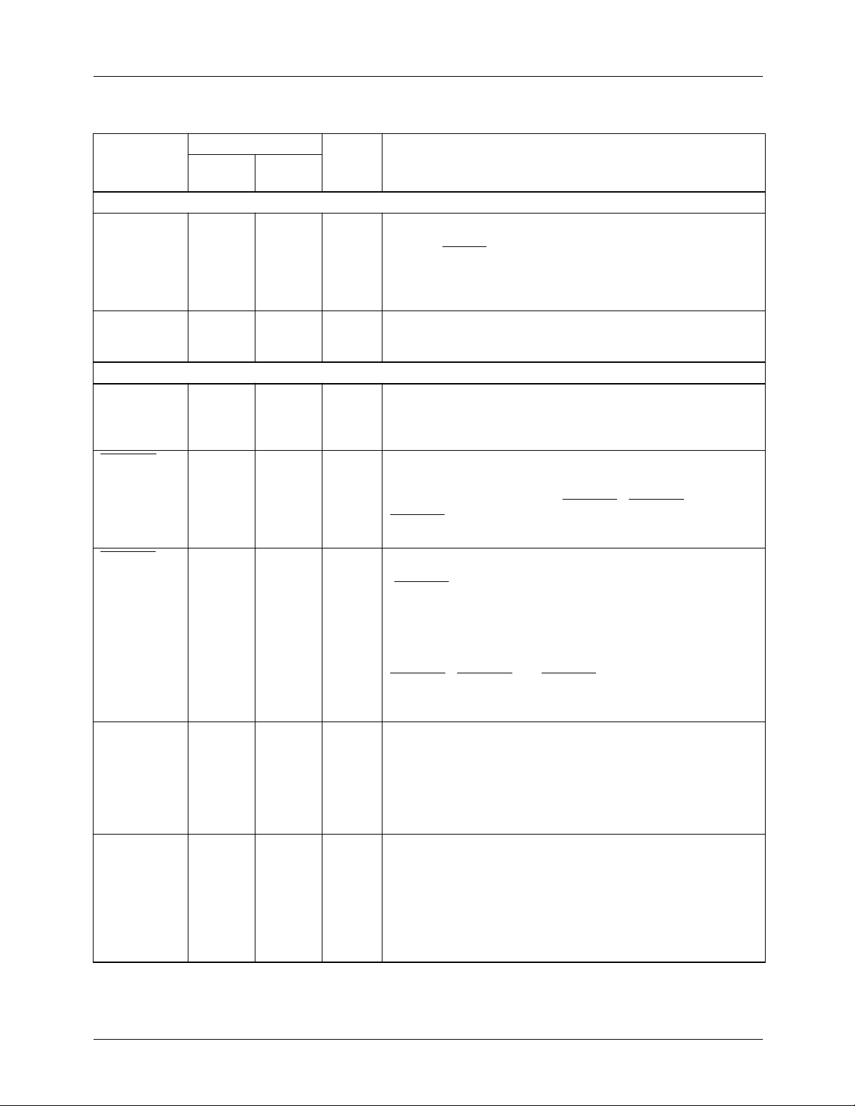
Pin Descriptions
Pin Name
Pin Number
Value Pin Function Description
84-Lead
PLCC 100-Lead
MQFP
Clocks
PXCK 79 60 TTL Master Clock Input. This 20 to 30 MHz clock is internally
divided by 2 to generate the internal pixel clock, PCK, which a
LOW on RESET forces LOW. PXCK drives the entire
TMC22x91, except the asynchronous microprocessor interface
and the semi-synchronous LDV data input clock. All internal
registers are strobed on the rising edge of PXCK.
LDV 78 59 TTL Pixel Data Load Clock. On each rising edge of LDV, data on
PD23-0 are latched into the input preload register, for transfer
into the input demultiplexer on the next rising edge of PCK.
Frame Buffer Interface
PD23-0 52-63,
66-77 26, 27,
31-40,
43-51,
56-58
TTL Pixel Data Inputs. In YCBCR, GBR, RGB, and color-indexed
mode, pixel data enter the TMC22x91 on PD23-0. The specific
format is found in Figures 1a and 1b. LDV is the clock that
controls the loading of pixel data.
VHSYNC 12 80 TTL Horizontal Sync I/O. In Master and Genlock modes, the
TMC22x91 outputs horizontal sync on this pin. In Slave modes,
the TMC22x91 accepts and locks to horizontal sync input on
this pin (with vertical sync on VVSYNC). VHSYNC and
VVSYNC must be coincident since they are clocked into the
TMC22x91 on the same rising edge of PXCK.
VVSYNC 13 81 TTL Vertical Sync I/O. In separate V and H sync Master and
Genlock modes, the TMC22x91 outputs vertical block sync
(VVSYNC LOW for the 2.5 (PAL) or 3 (NTSC) lines on which
vertical sync pulses occur). In composite sync (H and V sync
on same signal) Master and Genlock modes, the TMC22x91
outputs horizontal sync, vertical sync, and equalization over
this pin. In Slave mode, the TMC22x91 accepts and locks to
vertical sync input on this pin (with horizontal sync on
VHSYNC). VHSYNC and VVSYNC must be coincident such
that they are clocked into the TMC22x91 on the same rising
edge of PXCK.
PDC 11 77 TTL Pixel Data Control. In Master mode, the TMC22x91 forces
PDC HIGH when and only when it wants active video from the
frame buffer. During blanking (syncs, equalization, burst, and
porches), it forces PDC LOW, signaling that it will ignore any
data presented over PD23-0. When PDC is used as an input,
forcing it HIGH allows the TMC22x91 to receive PD during the
active video state.
KEY 4 70 TTL Hardware Key Input. When the HKEN control bit is set HIGH
and hardware key pin, KEY, is HIGH, video data entering on
CVBS7-0 are routed to the COMPOSITE output. This control
signal is pipelined so the pixel that is presented to the PD port
when the KEY signal is invoked is at the midpoint of the soft
key transition. When HKEN is LOW, KEY is ignored. Like PD
data, KEY is clocked into the TMC22x91 on the rising edge of
LDV.

TMC22091/TMC22191 PRODUCT SPECIFICATION
8
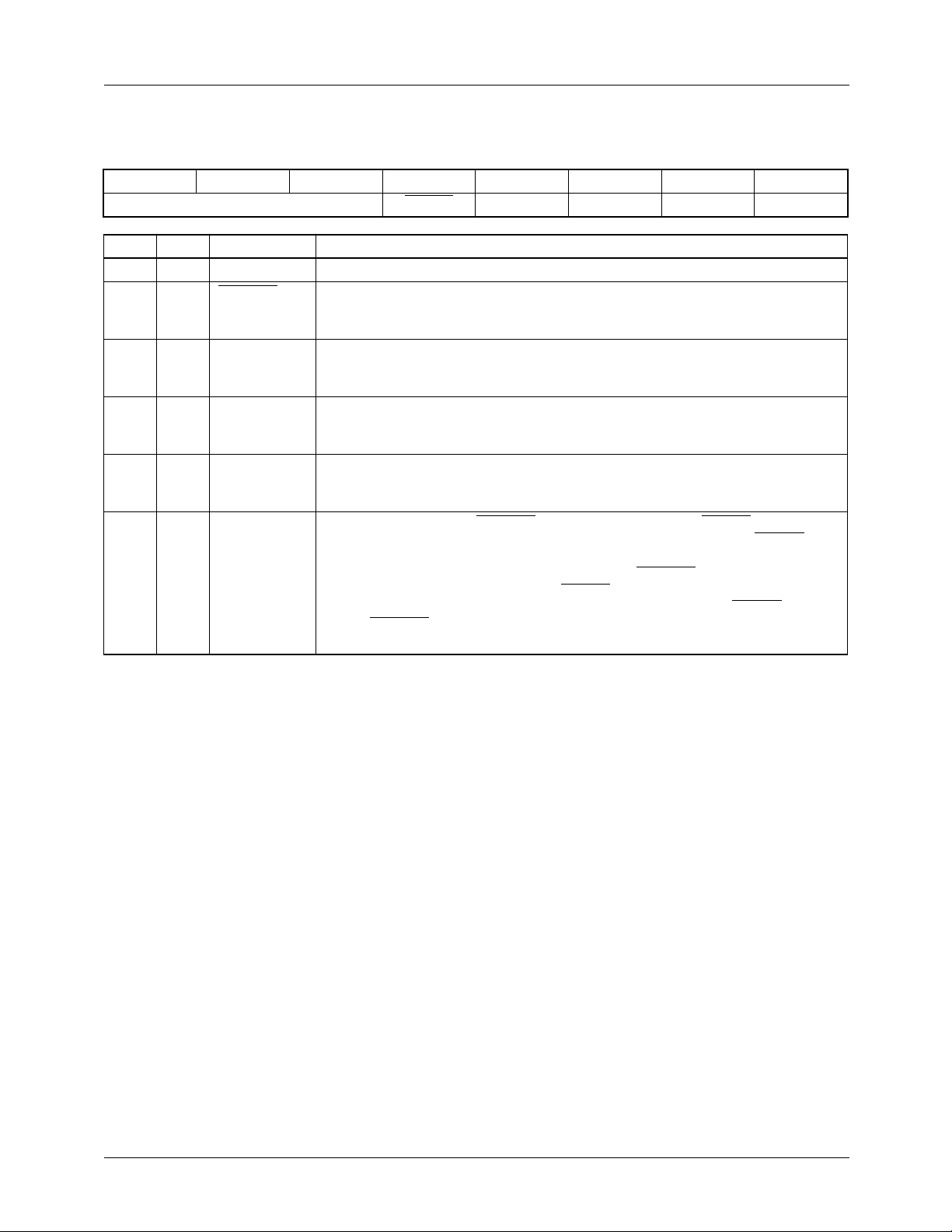
OL4-0 29, 48-51 97, 22-25 TTL Overlay Data Inputs (TMC22191 only). 30 of the 256
locations of the CLUT may be reserved for overlay operation.
These CLUT locations are directly accessed by five input pins,
OL4-0. OL4-0 are entered into the TMC22191 on a pixel-by-
pixel basis and select which of the 30 overlay colors is to be
encoded. When all five OL4-0 inputs are LOW, no overlay
occurs.
BYPASS 28 96 TTL CLUT Bypass Control (TMC22191 only). When BYPASS is
HIGH, the CLUT is in the pixel data path within the TMC22191.
When BYPASS is LOW, pixel data bypasses the CLUT.
BYPASS is active only for certain modes of the Layering
Control Register (LCR) when the Format Control Register bit 6
is HIGH.
Genlock Interface
GHSYNC 83 64 CMOS Genlock Horizontal Sync. In Genlock mode, the TMC22x91
will start a new horizontal line (blank-to-sync-edge transition)
with each falling edge of GHSYNC. In non-genlock modes, the
TMC22x91 ignores GHSYNC. The internal pixel clock, PCK, is
aligned with the falling edge of VHSYNC or GHSYNC (Genlock
mode).
GVSYNC 82 63 CMOS Genlock Vertical Sync. In Genlock mode, the TMC22x91 will
start a new vertical sync sequence at line 1 field 1 whenever
GVSYNC and GHSYNC are coincident such that they are
clocked into the TMC22x91 on the same rising edge of PXCK.
If GVSYNC falls at any other time, the TMC22x91 will assume
that this marks the start of field 2, and will ignore it (in odd-field
sync mode) or (in all-field sync mode) respond by generating a
single vertical sync pulse, followed by 2 (PAL) or 2.5 (NTSC)
lines of vertical sync, keyed to the next falling edge on
GHSYNC. See Interface Control Register bit 0 for odd-field and
all-field operation.
CVBS7-0 44-47,84,
1-3 18-21,
65-68 TTL Composite Video Inputs. The encoder receives digitized
video, subcarrier phase, and subcarrier frequency over this 8-
bit bus at the PCK rate. This data may be provided by the
companion TMC22071 Genlocking Video Digitizer. In Genlock
mode, the TMC22x91 expects subcarrier phase and frequency
data during each line’s horizontal sync interval, as well as video
data when keying is engaged, transferred at the PCK rate.
Microprocessor Interface
D7-0 14-21 82-89 TTL Data I/O Port. All control parameters are loaded into and read
back over this 8-bit port. For digital testing, the five lower bits
can also serve as a two-cycle 10-bit data output port. For D/A
converter testing, it can be used as a 10-bit two-cycle input
port, facilitating, for example, ramp-based D/A converter
linearity tests.
A1-0 8-9 74-75 TTL µProc Port Controls. As in a RAMDAC, this control governs
whether the microprocessor interface selects a table address
or reads/writes table contents. It also governs setting and
verification of the TMC22x91’s internal operating modes, also
over port D7-0.
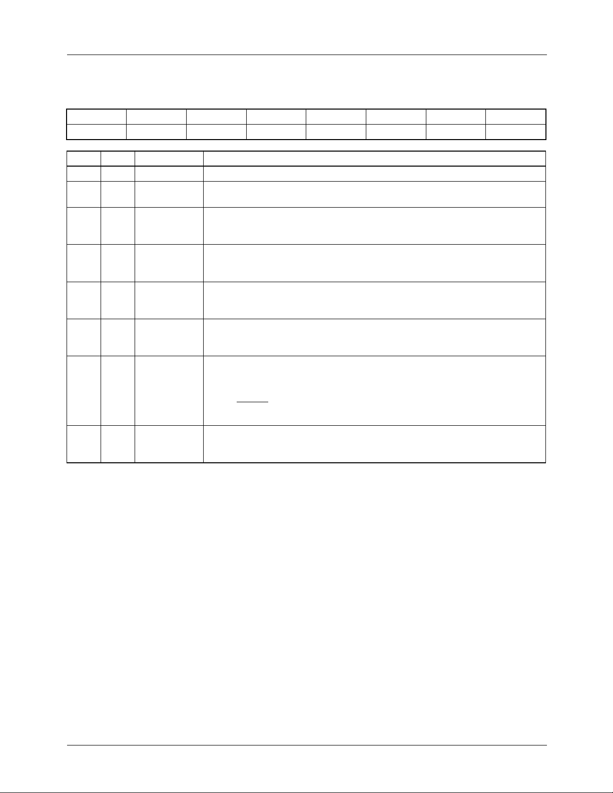
Pin Descriptions (continued)
Pin Name
Pin Number
Value Pin Function Description
84-Lead
PLCC 100-Lead
MQFP

PRODUCT SPECIFICATION TMC22091/TMC22191
9
CS 6 72 TTL Chip Select. When CS is HIGH, the microprocessor interface
port, D7-0, is set to HIGH impedance and ignored. When CS is
LOW, the microprocessor can read or write parameters over
D7-0. One additional falling edge of CS is needed to move input
data to its assigned working registers.
R/W 7 73 TTL Bus Read/Write Control. When R/W and CS are LOW, the
microprocessor can write to the control registers or CLUT over
D7-0. When R/W is HIGH and CS is LOW, it can read the
contents of any CLUT address or control register over D7-0.
RESET 5 71 TTL Master Reset Input. Bringing RESET LOW sets the software
reset control bit, SRESET, LOW, forcing the internal state
machines to their starting states and disabling all outputs.
Bringing RESET HIGH synchronizes the internal pixel clock
(PCK = PXCK / 2) to maintain a defined pipeline delay through
the TMC22x91. If HRESET is set HIGH, the encoder is enabled
when RESET goes HIGH. If HRESET is LOW, the host restarts
the TMC22x91 by setting SRESET HIGH. RESET does not
affect the CLUT or the control registers, except SRESET.
Video Output
COMPOSITE 33 2 1 V P-P NTSC/PAL Video. Analog output of composite D/A converter,
nominally 1.35 volt peak-to-peak into a 37.5Ωload.
LUMA 35 5 1 V P-P Luminance-only Video. Analog output of luminance D/A
converter, nominally 1.35 volt peak-to-peak into a 37.5Ωload.
CHROMA 37 8 1 V P-P Chrominance-only Video. Analog output of chrominance D/A
converter, nominally 1.35 volt peak-to-peak into a 37.5Ωload.
Analog Interface
VREF 30 98 +1.23 V Voltage Reference Input. External voltage reference input,
internal voltage reference output, nominally 1.235 V.
COMP 39 10 0.1 µFCompensation Capacitor. Connection point for 0.1µf
decoupling capacitor.
RREF 31 99 392ΩCurrent-setting Resistor. Connection point for external
current-setting resistor for D/A converters. The resistor (392Ω)
is connected between RREF and AGND. Output video levels
are inversely proportional to the value of RREF.
JTAGTest Interface
TDI 25 93 TTL Data Input Port. Boundary scan data input port.
TMS 24 92 TTL Scan Select Input. Boundary scan (HIGH)/normal operation
(LOW) selector.
TCK 23 91 TTL Scan Clock Input. Boundary scan clock.
TDO 22 90 TTL Data Output Port. Boundary scan data output port.
Power Supply
VDD 27, 64, 81 41, 62, 95 +5 V Positive digital power supply.
VDDA 40-43 13-17 +5 V Positive analog power supply.
DGND 10,26,65,
80 42,61,76,
94 0.0 V Digital Ground.
AGND 32,34,36,
38 4, 6, 9,
100 0.0 V Analog Ground.
Pin Descriptions (continued)
Pin Name
Pin Number
Value Pin Function Description
84-Lead
PLCC 100-Lead
MQFP

PRODUCT SPECIFICATION TMC22091/TMC22191
10
Control Registers
Test
TEST 28, 29,
48-51 22-25,
96-97 0.0 V Factory testing (TMC22091 only). Reserved for factory
testing. These pins have no effect on the operation but do
function as JTAG registers. They should be grounded directly
or pulled down to ground with 1kΩor smaller resistors.
NC N/A 1, 3, 7,
11-12,
28-30,
52-55,
69, 78-79
No Connect
Pin Descriptions (continued)
Pin Name
Pin Number
Value Pin Function Description
84-Lead
PLCC 100-Lead
MQFP
The TMC22x91 is initialized and controlled by a set of regis-
ters. The registers are organized into 13 categories:
1. Global Control
2. Format Control
3. Interface Control
4. Test Control
5. Key Control
6. Misc. Control
7. Standards Control
8. Layering Control (TMC22191)
9. Key Value
10. Timing
11. Subcarrier
12. Test I/O
13. Mask Register
An external controller loads the Control Registers through a
standard interface port. It also loads the CLUT and reads its
contents or those of the Control Registers. The port is
governed by pins CS, R/W, and A1-0.
TheAddress Register for the CLUT and the Control Register
pointer automatically increment to allow successive writes to
sequential addresses. In the CLUT, the Address Register has
two additional bits which increment in modulo-three to
sequentially access the red, green, and blue portions. All
three colors must be written when any CLUT address is
changed.
The control register autoincrement follows the sequence
indicated in the Control Register Map. When it reaches
address 40, it stops incrementing, allowing multiple reads or
writes of test data from/to the TESTDAT register. To exit the
test mode, reset the Control Register pointer by settingA1-0,
D7-0, and R/W LOW and then bring CS LOW.Address 1F is
a read-only status register. It is addressed by the autoincre-
ment sequencer. Any data may be written into this port at
that time but it will not be stored. When address 50 is
accessed, no autoincrement takes place, allowing multiple
writes to the Mask Register.

PRODUCT SPECIFICATION TMC22091/TMC22191
11
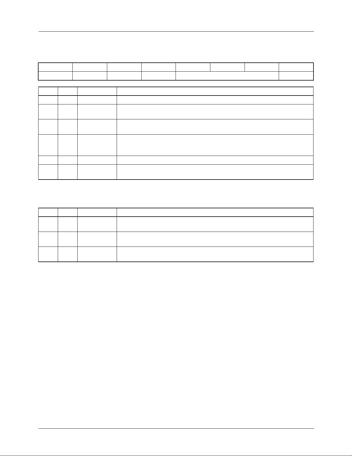
Table 2. Microprocessor Port Control
A1-0 R/W Action
00 0 Write D7-0 into Control Register
pointer
00 1 Read Control Register pointer
on D7-0
01 0 Write D7-0 into CLUT Address
Pointer
01 1 Read CLUT Address Pointer on
D7-0
10 0 WriteD7-0 to addressed Control
Register
10 1 Read addressed Control
Register on D7-0
11 0 Write D7-0 to addressed CLUT
location
11 1 Read addressed CLUT location
on D7-0
Table 3. Control Register Map
Reg Bit Name Function
Global Control Register
00 7-5 Reserved
00 4 SRESET Software reset
00 3 PAL Standard select, NTSC
or PAL
00 2 LUMDIS Luminance input disable
00 1 CHRDIS Chrominance input
disable
00 0 HRESET Software reset disable
Format Control Register
01 7 Reserved
01 6 LCREN Layering Control
Register enable
(TMC22191)
01 5 RAMPEN Modulated ramp test
01 4 CB Color bar test
01 3-2 FORMAT PD23-0 input format
select
01 1-0 INMODE PD23-0 input mode
select
Interface Control Register
02 7 VITSEN VITS lines enable
02 6 SHCY Short-cycle test mode
02 5-4 TBASE Time-base source select
02 3 SOUT Sync output mode select
02 2 FBDIS Frame buffer signals
disable
02 1 PDCDIR PDC master, slave
select
02 0 FLDLK Field lock select
Test Control Register
03 7 Reserved
03 6 LIMEN Luminance limiter
enable
03 5 TESTEN Test enable
03 4 HOLDEN MSBs/LSBs hold select
03 3 TSTMSB LSBs, MSBs in/out
select
03 2 LUMTST LUMA channel test
03 1 8FSUBR 8-field subcarrier reset
enable
03 0 CHRTST CHROMA channel test
Key Control Register
04 7 Reserved
04 6 HKEN Hardware key enable
04 5 BUKEN Burst key enable
04 4 SKEXT Data key operation
select
04 3 DKDIS Green/red/Y data key
disable
04 2 EKDIS Blue/green/CBdata key
disable
04 1 FKDIS Red/blue/CRdata key
disable
04 0 SKEN Data key enable
Layering Control Register (TMC22191)
04 7 LAYMODE MSB of Layer
Assignments select
04 6 HKEN Hardware key enable
04 5 BUKEN Burst key enable
04 4 SKEXT Data key operation
select
04 3-1 LAYMODE LSBs of Layer
Assignments select
04 0 SKEN Data key enable
KeyValue Registers
05 7-0 DKEY Green/red/Y data key
value
06 7-0 EKEY Blue/green/CBdata key
value
Table 3. Control Register Map (continued)
Reg Bit Name Function

TMC22091/TMC22191 PRODUCT SPECIFICATION
12
07 7-0 FKEY Red/blue/CRdata key
value
08-0D Reserved
Misc. Control Register
0E 7 EFEN Register 0E and 0F
enable
0E 6 COMPD/A COMPOSITE D/A
disable
0E 5 SVIDD/A LUMA/CHROMA D/A
disable
0E 4 FKREN Luminance processing
enabled
0E 3 RATIO Luminance ratio select
0E 2 TFLK Luminance pass
threshold select
0E 1 T512 EH/SL offset select
0E 0 CB100 NTSC/PAL Color Bars
Standards Control Register
0F 7 EFEN Same as Reg 0E bit 7
but read-only
0F 6 SIX25 625/525 line per frame
select
0F 5 PALID Phase alternate line
select
0F 4 SETUP 7.5 IRE Pedestal Enable
0F 3-2 YGAIN Luminance gain settings
0F 1-0 CGAIN Chrominance gain
settings
Timing Registers
10 7-0 SY Horizontal sync tip
length
11 7-0 BR Breezeway length
12 7-0 BU Burst length
13 7-0 CBP Color back porch length
14 7-0 XBP Extended color back
porch 8 LSB
15 7-0 VA Active video 8 LSB
16 7-0 VC Active video start 8 LSB
17 7-0 VB Active video end 8 LSB
18 7-6 XBP Extended color back
porch 2 MSB
18 5-4 VA Active video 2 MSB
18 3-2 VC Active video start 2 MSB
18 1-0 VB Active video end 2 MSB
Table 3. Control Register Map (continued)
Reg Bit Name Function
Notes:
1. Functions are listed in the order used for reading and
writing.
2. For each register listed above, all bits not listed are
reserved and should be set to zero to ensure proper
operation.
3. The meaning of Register 04 (Key Control Register/Layer-
ing Control Register) is determined by Format Control
Register bit 6 (TMC22191).
19 7-0 FP Front porch length
1A 7-0 EL Equalization pulse LOW
length
1B 7-0 EH Equalization pulse HIGH
length
1C 7-0 SL Vertical sync LOW
length
1D 7-0 SH Vertical sync HIGH
length
1E 7-0 CBL Color bar length
1F 7-5 FIELD Field identification
1F 4-0 LTYPE Line type identification
Subcarrier Registers
20 7-0 FREQL Subcarrierfrequency4th
byte (LSBs)
21 7-0 FREQ3 Subcarrierfrequency3rd
byte
22 7-0 FREQ2 Subcarrier frequency
2nd byte
23 7-0 FREQM Subcarrierfrequency 1st
byte (MSBs)
24 7-0 SYSPHL Video phase offset LSBs
25 7-0 SYSPHM Video phase offset
MSBs
26 7-0 BURPHL Burst phase offset LSBs
27 7-0 BURPHM Burst phase offset MSBs
28-3F Reserved
Test I/O Register
40 7-0 TESTDAT Test data input/output
Mask Register
50 7-0 MASK Mask register
Y-Component Register
60 7-0 Y Y-component input/
output
Table 3. Control Register Map (continued)
Reg Bit Name Function
PRODUCT SPECIFICATION TMC22091/TMC22191
13
Control Register Definitions
Global Control Register (00)
76543210
Reserved SRESET PAL LUMDIS CHRDIS HRESET
Reg Bit Name Function
00 7-5 Reserved.
00 4 SRESET Software reset. When LOW, resets and holds internal state machines and
disables outputs. When HIGH (normal), starts and runs state machines and
enables outputs.
00 3 PAL Video standard select. When LOW, the NTSC standard is generated with 7.5
IRE pedestal. When HIGH, PAL standard video is generated. This bit is ignored
if Register 0E bit 7 is HIGH, enabling the 0E and 0F registers.
00 2 LUMDIS Luminance input disable. When LOW (normal), luminance (Y) data from
external frame buffer is enabled. When HIGH, luminance (Y) data into the
TMC22x91 is forced to 0 IRE but sync pulses continue from the LUMA output.
00 1 CHRDIS Chrominance input disable. When LOW (normal), burst and frame buffer data
into the TMC22x91 are enabled. when HIGH, burst and frame buffer data are
suppressed, enabling monochrome operation.
00 0 HRESET Software reset enable. SRESET is forced LOW when the RESET pin is taken
LOW. State machines are reset and held. When HRESET is LOW, RESET may
be taken HIGH at any time. The TMC22x91 is enabled and a new frame is
begun with line 1, field 1 on the next PXCK after SRESET is set HIGH. The D/A
converters are powered down while RESET is LOW. When HRESET is HIGH,
a new frame is begun with line 1, field 1 on the next PXCK after RESET is taken
HIGH. SRESET is ignored. The D/A converters remain active during the reset
sequence.

TMC22091/TMC22191 PRODUCT SPECIFICATION
14
Control Register Definitions (continued)
Format Control Register (01)
76543210
Reserved LCREN RAMPEN CB FORMAT INMODE
Reg Bit Name Function
01 7 Reserved.
01 6 LCREN (TMC22191) Layering Control Register enable. When LOW, the Layering
Control Register is not available and Key Control Register functions are
enabled. In this mode, the TMC22191 functions like the TMC22091. When
HIGH, the Layering Control Register takes the place of the Key Control
Register and enables the layering functions. Data loaded into the Key or
Layering Control Registers will remain but have a different meaning if this bit is
changed.
01 5 RAMPEN Modulated ramp test. When LOW (normal), the TMC22x91 encodes and
outputs video corresponding to input data. When RAMPEN and CB are both
HIGH, an internally generated 40 IRE modulated ramp is produced, preempting
input data.
01 4 CB Color bar test. When HIGH (normal), the TMC22x91 encodes and outputs
video corresponding to input data. When CB, RAMPEN, and Format Control
Register bit 0 are LOW, internally generated color bars are produced,
preempting input data.
01 3-2 FORMAT PD23-0 input format select. Two bits select RGB, GBR, or YCBCRinput data.
When bits 3 and 2 are:
0 0 the CLUT output is interpreted as RGB and is converted to YCBCR.
0 1 is reserved. Bits 3 and 2 must be 00 or 10 when the Layering Control
Register is enabled (TMC22191).
1 0 the CLUT output is interpreted as GBR, and is converted to YCBCR.
1 1 the CLUT output is interpreted as YCBCR.
01 1-0 INMODE PD23-0 input mode select. These two bits set up the TMC22x91 for either 444,
422, 15-bit, or 8-bit input modes.
0 0 24-bit/pixel GBR, RGB, or YCBCR444 data enters from PD23-0
0 1 YCBCR422 data enters from PD23-8; CRand CBalternate from PD15-8
1 0 15-bit/pixel GBR or RGB data from PD14-0
1 1 8-bit/pixel color indexed data enters from PD7-0.
Bits 1 and 0 must be 00, 01, or 11 when the Layering Control Register is
enabled (TMC22191).

PRODUCT SPECIFICATION TMC22091/TMC22191
15
Control Register Definitions (continued)
Interface Control Register (02)
76543210
VITSEN SHCY TBASE SOUT FBDIS PDCDIR FLDLK
Reg Bit Name Function
02 7 VITSEN VITS lines enable. When LOW, all UBB lines in the vertical interval are black
burst regardless of input data. When HIGH, all UBB lines in the vertical interval
become UVV active video and are dependent upon input data.
02 6 SHCY Short-cycle test mode. When LOW, normal operation is enabled. when HIGH,
EH (equalization pulse HIGH length) and SL (vertical sync LOW length) are
shortened by 256.
02 5-4 TBASE Time-base source select. These two bits set up the TMC22x91 for either
genlock or frame buffer control of timing. When bits 5 and 4 are:
0 0 the encoder counts out its own time-base from input clock PXCK.
0 1 the encoder locks to synchronizing signals from external genlock.
1 0 the encoder locks to synchronizing signals from frame buffer controller.
02 3 SOUT Sync output mode select. When LOW, VHSYNC and VVSYNC output separate
horizontal and vertical sync pulses. When HIGH, composite sync (H and V) is
output on VVSYNC while horizontal sync is output on VHSYNC.
02 2 FBDIS Frame buffer signals enable. When LOW, VVSYNC and VHSYNC outputs to
frame buffer are enabled. When HIGH, VVSYNC and VHSYNC outputs to
frame buffer are disabled.
02 1 PDCDIR PDC master/slave select. When LOW, PDC is an output where the encoder is
requesting data from the frame buffer. When HIGH, PDC is an input, and
directs the encoder to accept data from the frame buffer.
02 0 FLDLK Field lock select. When LOW, (in Slave mode) the encoder locks to each new
field. When HIGH, the encoder locks to field 1 only.
TMC22091/TMC22191 PRODUCT SPECIFICATION
16
Control Register Definitions (continued)
Test Control Register (03)
76543210
Reserved LIMEN TESTEN HOLDEN TSTMSB LUMTST 8FSUBR CHRTST
Reg Bit Name Function
03 7 Reserved.
03 6 LIMEN Luminance limiter enable. When LOW, all luminance values are passed to
modulator. when HIGH, luminance values are limited to 101 IRE.
03 5 TESTEN Test enable. When LOW, normal operation is enabled. When HIGH,
TESTDAT7-0 (Register 40) is connected to the composite output (READ) and
D/A converters (WRITE) for test.
03 4 HOLDEN MSBs/LSBs hold select. When LOW, alternates MSBs and LSBs in test, at
PXCK rate. When HIGH, reads/writes only MSBS or LSBS in test (per
TSTMSB, bit 3)
03 3 TSTMSB LSBS,MSBS hold select. When LOW, connects 2 LSBs to TESTDAT1-0
for testing when TESTEN is HIGH. When HIGH, connects 8 MSBs to
TESTDAT7-0 for testing when TESTEN is HIGH.
03 2 LUMTST LUMA channel test. When LOW (normal), the luminance D/A converter is
driven from luminance channel. When HIGH, the luminance D/A converter is
driven from TESTDAT for testing when TESTEN is HIGH.
03 1 8FSUBR 8-field subcarrier reset enable. When LOW, the internal subcarrier generator is
reset with frequency and phase data from FREQ, SYSPH, and BURPH
registers every eight fields. When HIGH, the internal subcarrier generator free-
runs on the basis of frequency and phase data from the last time it was reset.
When RESET goes LOW, the subcarrier frequency and phase will be reset
from FREQ, SYSPH, and BURPH after field 8.
03 0 CHRTST CHROMA channel test. When LOW (normal), the chrominance D/A converter is
driven from chrominance channel. When HIGH, the chrominance D/A converter
is driven from TESTDAT when TESTEN is HIGH.

PRODUCT SPECIFICATION TMC22091/TMC22191
17
Control Register Definitions (continued)
Key Control Register (04)
76543210
Reserved HKEN BUKEN SKEXT DKDIS EKDIS FKDIS SKEN
Reg Bit Name Function
04 7 Reserved.
04 6 HKEN Hardware key enable. When LOW, the KEY input pin ignored. When HIGH, the
KEY input pin is enabled.
04 5 BUKEN Burst key enable. When LOW, output video burst is generated on TMC22x91.
When HIGH, output burst is taken from genlock input data.
04 4 SKEXT Data key operation select. When LOW, data keying is allowed only during
active video. When HIGH, keying is allowed during active video and blanking.
04 3 DKDIS Green/red/Y data key disable. When LOW, green/red/Y input data is enabled
for data keying. When HIGH, green/red/Y input data is ignored for data keying.
This function is enabled when Layering Control Register is enabled
(TMC22191).
04 2 EKDIS Blue/green/CBdata key disable. When LOW, Blue/green/CBinput data is
enabled for data keying. When HIGH, Blue/green/CBinput data is ignored for
data keying. This function is enabled when Layering Control Register is
enabled (TMC22191).
04 1 FKDIS Red/blue/CRdata key disable. When LOW, red/blue/CRinput data is enabled
for data keying. When HIGH, red/blue/CRinput data is ignored for data keying.
This function is enabled when Layering Control Register is enabled
(TMC22191).
04 0 SKEN Data key enable. When LOW, data keying is disabled. When HIGH, data keying
is enabled.
TMC22091/TMC22191 PRODUCT SPECIFICATION
18
Control Register Definitions (continued)
Layering Control Register (04) (TMC22191)
76543210
LAYMODE HKEN BUKEN SKEXT LAYMODE SKEN
Reg Bit Name Function
04 7 LAYMODE MSB of Layer Assignments select.
04 6 HKEN Hardware key enable. When LOW, the KEY input pin ignored. When HIGH, the
KEY input pin is enabled.
04 5 BUKEN Burst key enable. When LOW, output video burst is generated on TMC22191.
When HIGH, output burst is taken from genlock input data.
04 4 SKEXT Data key operation select. When LOW, data keying is allowed only during
active video. When HIGH, data keying is allowed during active video and
blanking.
04 3-1 LAYMODE Three LSBs of Layer Assignments select.
04 0 SKEN Data key enable. When LOW, data keying is disabled. When HIGH, data keying
is enabled.
KeyValue Registers (05-07)
Reg Bit Name Function
05 7-0 DKEY Green/red/Y data key value. Eight bits hold the match value which triggers
keying on red/Y.
06 7-0 EKEY Blue/green/U data key value. Eight bits hold the match value which triggers
keying on green/U.
07 7-0 FKEY Red/blue/V key value. Eight bits hold the match value which triggers keying on
blue/V.

PRODUCT SPECIFICATION TMC22091/TMC22191
19
Control Register Definitions (continued)
Miscellaneous Control Register (0E)
76543210
EFEN COMPD/A SVIDD/A FKREN RATIO TFLK T512 CB100
Reg Bit Name Function
0E 7 EFEN Register 0E and 0F enable. When LOW, the functions of Register 0E and 0F
are disabled. When HIGH, Registers 0E and 0F are active. When Registers 0E
and 0F are enabled, Register 00 bit 3 is ignored. Register 0E bit 7 will read back
whatever value was written.
0E 6 COMPD/A COMPOSITE D/A disable. When HIGH, the COMPOSITE D/A converter is
powered-down. When LOW, the D/A is enabled.
0E 5 SVIDD/A LUMA/CHROMA D/A disable. When HIGH, the LUMA and CHROMA D/A
converters are powered-down. When LOW, they are enabled.
0E 4 FKREN Luminance processing enable. When FKREN is HIGH, the KEY input defines
the function of CVBS input data. When the KEY input is HIGH, CVBS data is
keyed over PD input data. When KEY is LOW, CVBS data is assumed to be
luminance data delayed by one When FKREN is LOW, the KEY input operates
normally, switching between CVBS and PD data.
0E 3 RATIO Luminance ratio control bit. When LOW, 1/2 of current luminance and 1/2 of
field delayed luminance from the CVBS input are added to yield a new
combined luminance value. When RATIO is HIGH, 3/4 of current luminance is
added to 1/4 of the delayed luminance to produce a new luminance value.
0E 2 TFLK Luminance-pass threshold. The difference between current luminance and
delayed luminance (from the CVBS inputs) is compared against a preset
threshold set by TFLK. When TFLK is LOW, the high threshold must be
exceeded to trigger the combining of current and delayed luminance (according
to RATIO). If the higher threshold is not exceeded, current luminance is passed
without modification. When TFLK is HIGH, a lower threshold is used to trigger
the combining of current and delayed luminance.
0E 1 T512 EH/SL offset control bit. When LOW, the true value of EH and SL is offset by
256. When HIGH, the true value for EH and SL is offset by 512.
0E 0 CB100 NTSC/PAL color bars select. When HIGH, color bars with 100% white level are
selected. When LOW, color bars will have 75% white level.

TMC22091/TMC22191 PRODUCT SPECIFICATION
20
Control Register Definitions (continued)
Standards Control Register (0F)
76543210
EFEN SIX25 PALID SETUP YGAIN CGAIN
Reg Bit Name Function
0F 7 EFEN Same as Register 0E bit 7, but read-only.
0F 6 SIX25 Select 625 lines per frame. When HIGH, the encoder assumes 625 line per
frame. When LOW, 525 lines per frame are assumed.
0F 5 PALID PAL select. When HIGH, Phase alternate line (PAL) operation is selected.
When LOW, operation conforms to NTSC standards.
0F 4 SETUP Setup enable. When HIGH, a 7.5 IRE Pedestal is added to the output video.
when LOW, no pedestal is added.
0F 3-2 YGAIN Luminance gain settings are adjusted to conform to the following NTSC and
PAL standards:
0 0 NTSC without SETUP
0 1 NTSC-A and PAL-M
1 0 PAL-I and PAL-N
1 1 Reserved
0F 1-0 CGAIN Chrominance gain settings are adjusted to conform to the following NTSC and
PAL standards:
0 0 NTSC without SETUP
0 1 NTSC-A and PAL-M
1 0 PAL-I and PAL-N
1 1 Reserved
Timing Registers (10-17)
Reg Bit Name Function
10 7-0 SY Horizontal sync tip length. This 8-bit register holds a value extending from 0 to
255 PCK cycles.
11 7-0 BR Breezeway length. This 8-bit register holds a value extending from 0 to 255
PCK cycles.
12 7-0 BU Burst length. This 8-bit register holds a value extending from 0 to 255 PCK
cycles.
13 7-0 CBP Color back porch length. This 8-bit register holds a value extending from 0 to
255 PCK cycles.
14 7-0 XBP Extended color back porch 8 LSBs. This 8-bit register holds the LSBs of a
10-bit value extending from 0 to 1023 PCK cycles. The two MSBs are located in
control register 18.
15 7-0 VA Active video 8 LSBs. This 8-bit register holds the LSBs of a 10-bit value
extending from 0 to 1023 PCK cycles. The two MSBs are located in control
register 18.
16 7-0 VC Active video start 8 LSBs. This 8-bit register holds the LSBs of a 10-bit value
which is the initial half active video length extending from 0 to 1023 PCK cycles.
The two MSBs are located in control register 18.
17 7-0 VB Active video end 8 LSBs This 8-bit register holds the LSBs of a 10-bit value
which is the end half active video length extending from 0 to 1023 PCK cycles.
The two MSBs are located in control register 18.
This manual suits for next models
1
Table of contents
Other Exar Recording Equipment manuals


