Exar XRT73L03 User manual
Exar Corporation 48720 Kato Road, Fremont CA, 94538 •(510) 668-7000 •FAX (510) 668-7017 •www.exar.com
áç
áçáç
áç XRT73L03
3 CHANNEL DS3/E3/STS-1 LINE INTERFACE UNIT
MARCH 2001 REV. 1.1.0
GENERAL DESCRIPTION
The XRT73L03, 3-Channel, DS3/E3/STS-1 Line In-
terface Unit consists of three independent line trans-
mitters and receivers integrated on a single chip de-
signed for DS3, E3 or SONET STS-1 applications.
Each channel of the XRT73L03 can be configured to
support the E3 (34.368 Mbps), DS3 (44.736 Mbps) or
the SONET STS-1 (51.84 Mbps) rates. Each channel
can be configured to operate in a mode/data rate that
is independent of the other channels.
In the transmit direction, each channel encodes input
data to either B3ZS (DS3/STS-1) or HDB3 (E3) for-
mat and converts the data into the appropriate pulse
shapes for transmission over coaxial cable via a 1:1
transformer.
In the receive direction, the XRT73L03 performs
equalization on incoming signals, performs Clock Re-
covery, decodes data from either B3ZS or HDB3 for-
mat, converts the receive data into TTL/CMOS for-
mat, checks for LOS or LOL conditions and detects
and declares the occurrence of Line Code Violations.
FEATURES
•Meets E3/DS3/STS-1 Jitter Tolerance Require-
ments
•Contains a 4-Wire Microprocessor Serial Interface
•Full Loop-Back Capability
•Transmit and Receive Power Down Modes
•Full Redundancy Support
•Uses Minimum External components
•Single +3.3V Power Supply
•5V tolerant I/O
•-40°C to +85°C Operating Temperature Range
•Available in a Thermally Enhanced 120 pin TQFP
package
APPLICATIONS
•Digital Cross Connect Systems
•CSU/DSU Equipment
•Routers
•Fiber Optic Terminals
•Multiplexers
•ATM Switches
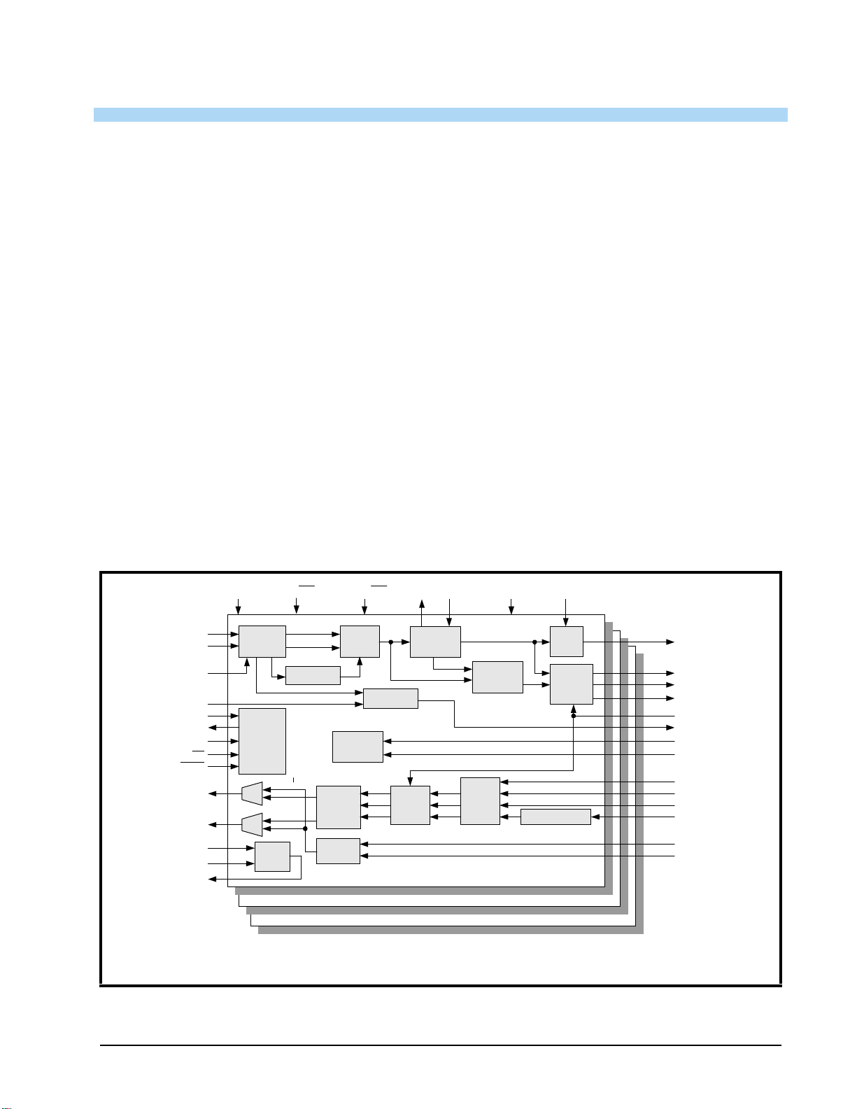
FIGURE 1. XRT73L03 BLOCK DIAGRAM
ENDECDIS
RLOS_(n)
LLB_(n)
RLB_(n)
TAOS_(n)
TPData_(n)
TNData_(n)
TxClk_(n)
TxLEV_(n)
TxOFF_(n)
Channel 2 - (n) = 2
AGC/
Equalizer
Serial
Processor
Interface
Peak
Detector
LOS Detector
Slicer Clock
Recovery
Data
Recovery
Invert
Loop MUX
HDB3/
B3ZS
Decoder
LOSTHR_(n)
SDI
SDO
SClk
CS
REGR
RTIP_(n)
RRing_(n)
REQEN_(n)
Channel 0 - (n) = 0
Channel 1 - (n) = 1
Notes: 1. (n) = 0, 1, or 2 for respective Channels
2. Serial Processor Interface input pins are shared by the three Channels in HOST Mode and redefined in Hardware Mode.
Device
Monitor
MTIP_(n)
MRing_(n)
DMO_(n)
Transmit
Logic Duty Cycle Adjust
TTIP_(n)
TRing_(n)
Pulse
Shaping
HDB3/
B3ZS
Encoder
E3_(n) STS-1/DS3_(n) Host/(HW) RLOL_(n) EXClk_(n) RxOFF RxClkINV
RxClk_(n)
RPOS_(n)
RNEG_(n)
LCV_(n)
Tx
Control

XRT73L03 áç
áçáç
áç
3 CHANNEL DS3/E3/STS-1 LINE INTERFACE UNIT
REV. 1.1.0
2
TYPICAL APPLICATIONS
TRANSMIT INTERFACE CHARACTERISTICS:
•Accepts either Single-Rail or Dual-Rail data from
Terminal Equipment and generates a bipolar signal
from the line
•Integrated Pulse Shaping Circuit
•Built-in B3ZS/HDB3 Encoder (which can be dis-
abled)
•Contains Transmit Clock Duty Cycle Correction Cir-
cuit on-chip
•Generates pulses that comply with the ITU-T G.703
pulse template (E3 applications)
•Generates pulses that comply with the DSX-3 pulse
template as specified in Bellcore GR-499-CORE
and ANSI T1.102_1993
•Generates pulses that comply with the STSX-1
pulse template as specified in Bellcore GR-253-
CORE
•Transmitter can be turned off in order to support
redundancy designs
RECEIVE INTERFACE CHARACTERISTICS:
•Integrated Adaptive Receive Equalization (optional)
and Timing Recovery
•Declares and Clears the LOS defect per ITU-T
G.775 requirements (E3 and DS3 applications)
•Meets Jitter Tolerance Requirements as specified in
ITU-T G.823_1993 (E3 Applications)
•Meets Jitter Tolerance Requirements as specified in
Bellcore GR-499-CORE (DS3 Applications)
•Declares Loss of Signal (LOS) and Loss of Lock
(LOL) Alarms
•Built-in B3ZS/HDB3 Decoder (which can be dis-
abled)
•Recovered Data can be muted while the LOS Con-
dition is declared
•Outputs either Single-Rail or Dual-Rail data to the
Terminal Equipment
•Receiver can be powered down in order to con-
serve power in redundancy designs
FIGURE 2. MULTICHANNEL ATM APPLICATION
ATM
Switch/
SAR XRT72L73
RPOS
RNEG
RxLineClk
XRT71D03 XRT73L03
RRPOS
RRNEG
RRClk
RPOS
RNEG
RxClk
RPOS
RNEG
RxClk
RTIP
RRing
TTIP
TRing
TPOS
TNEG
TxLineClk
MClk TPOS
TNEG
TxClk
3 Channel DS3 ATM UNI 3 Channel E3/DS3 J/A 3 Channel E3/DS3 LIU
FIGURE 3. MULTISERVICE - FRAME RELAY APPLICATION
Frame
Relay XRT72L56
RPOS
RNEG
RxLineClk
XRT71D03 XRT73L03
RRPOS
RRNEG
RRClk
RPOS
RNEG
RxClk
RPOS
RNEG
RxClk
RTIP
RRing
TTIP
TRing
TPOS
TNEG
TxLineClk
MClk
TPOS
TNEG
TxClk
6 Channel E3/DS3 Framer 2 x 3 Channel E3/DS3 J/A 2 x 3 Channel E3/DS3 LIU

áç
áçáç
áç XRT73L03
3 CHANNEL DS3/E3/STS-1 LINE INTERFACE UNIT
REV. 1.1.0
3
ORDERING INFORMATION
FIGURE 4. PIN OUT OF THE XRT73L03 IN THE 120 PIN TQFP PACKAGE
1
2
3
4
5
6
7
8
9
10
11
12
13
14
15
16
17
18
19
20
21
22
23
24
25
26
27
28
29
30
31
32
33
34
35
36
96
95
94
93
92
91
90
89
88
87
86
85
84
83
82
81
80
79
78
77
76
75
74
73
72
71
70
69
68
67
66
65
64
63
62
61
97
98
99
100
101
102
103
104
105
106
107
108
109
110
111
112
113
114
115
116
117
118
119
120
60
59
58
57
56
55
54
53
52
51
50
49
48
47
46
45
44
43
42
41
40
39
38
37
XRT73L03
RLOL_2
LCV_2
RLOS_2
RLOL_0
LCV_0
RLOS_0
RxDGND_0
NC
NC
RPOS_0
RNEG_0
RxClk_0
RxDVDD_0
EXClk_0
RxDGND_2
RPOS_2
RNEG_2
RxClk_2
HOST/(HW)
RxDVDD_2
AGND_0
TxAGND_0
DMO_0
TxAVDD_0
REGR/(RxClkINV)
STS-1/DS3_1
AGND_2
SR/(DR)
E3_1
NC
NC
LOSTHR_1
LLB_1
RLB_1
RxAVDD_1
RRing_1
RTIP_1
RxAGND_1
REQEN_1
RxAGND_2
RTIP_2
RRing_2
RxAVDD_2
RLB_2
LLB_2
LOSTHR_2
REQEN_0
RxAGND_0
RTIP_0
RRing_0
RxAVDD_0
RLB_0
LLB_0
LOSTHR_0
ICT
STS-1/DS3_0
SDO/(E3_0)
SDI/(RxOFF_0)
SClk/(RxOFF_1)
CS/(ENDECDIS)
TNData_1
TPData_1
TxClk_1
MRing_1
MTIP_1
TAOS_1
TAOS_2
TxLEV_1
TxLEV_2
TTIP_1
TxAVDD_1
TRing_1
TxAGND_1
TxAGND_2
MRing_2
MTIP_2
TxAGND_2
TRing_2
TxAVDD_2
TTIP_2
DMO_2
TxAVDD_2
TNData_2
TPData_2
TxClk_2
TxAGND_0
TRing_0
TxAVDD_0
TTIP_0
MTIP_0
MRing_0
TNData_0
TPData_0
TxClk_0
TxLEV_0
TAOS_0
EXDGND
EXDVDD
EXClk_1
REQEN_2
STS1/DS3_2
E3_2
EXClk_2
RxOFF_2
RLOL_1
LCV_1
RLOS_1
RxDGND_1
RPOS_1
RNEG_1
RxClk_1
LOSMUTEN
RxDVDD_1
AGND_1
TxOFF_2
TxOFF_1
TxOFF_0
TxAGND_1
TxAVDD_1
DMO_1
PART #P
ACKAGE OPERATING TEMPERATURE RANGE
XRT73L03IV 120 Pin TQFP 14mm X 20mm -40oC to +85oC

XRT73L03 áç
áçáç
áç
3 CHANNEL E3/DS3/STS-1 LINE INTERFACE UNIT
REV. 1.1.0
I
TABLE OF CONTENTS
GENERAL DESCRIPTION ................................................................................................. 1
FEATURES .................................................................................................................................................... 1
APPLICATIONS ......................................................................................................................................... 1
TYPICAL APPLICATIONS ................................................................................................................................. 2
TRANSMIT INTERFACE CHARACTERISTICS: ..................................................................................................... 2
RECEIVE INTERFACE CHARACTERISTICS: ....................................................................................................... 2
ORDERING INFORMATION ............................................................................................... 3
PIN DESCRIPTIONS (BY FUNCTION) .............................................................................. 4
TRANSMIT INTERFACE ................................................................................................................................... 4
RECEIVE INTERFACE ..................................................................................................................................... 6
CLOCK INTERFACE ........................................................................................................................................ 7
OPERATING MODE SELECT ........................................................................................................................... 7
CONTROL AND ALARM INTERFACE ................................................................................................................. 9
MICROPROCESSOR INTERFACE .................................................................................................................... 11
POWER AND GROUND PINS ......................................................................................................................... 13
NOCONNECTION PINS ................................................................................................................................ 14
ELECTRICAL CHARACTERISTICS ................................................................................ 15
ABSOLUTE MAXIMUM RATINGS .................................................................................................................... 21
SYSTEM DESCRIPTION .................................................................................................. 23
THE TRANSMIT SECTION - CHANNELS 0, 1 AND 2 ......................................................................................... 23
THE RECEIVE SECTION - CHANNELS 0, 1 AND 2 ........................................................................................... 23
THE MICROPROCESSOR SERIAL INTERFACE ................................................................................................. 23
1.0 Selecting the Data Rate .................................................................................................................... 24
1.1 CONFIGURING CHANNEL(N) ............................................................................................................................... 24
2.0 The Transmit Section ....................................................................................................................... 26
COMMAND REGISTER, CR4-(N) ...................................................................................................... 26
2.1 THE TRANSMIT LOGIC BLOCK ............................................................................................................................ 26
2.1.1 Accepting Dual-Rail Data from the Terminal Equipment ...................................................................... 26
2.1.2 Accepting Single-Rail Data from the Terminal Equipment ................................................................... 27
COMMAND REGISTER CR1-(N) ....................................................................................................... 27
2.2 THE TRANSMIT CLOCK DUTY CYCLE ADJUST CIRCUITRY ................................................................................... 28
2.3 THE HDB3/B3ZS ENCODER BLOCK .................................................................................................................. 28
2.3.1 B3ZS Encoding .................................................................................................................................... 28
2.3.2 HDB3 Encoding .................................................................................................................................... 29
2.3.3 Disabling the HDB3/B3ZS Encoder ..................................................................................................... 29
COMMAND REGISTER CR2-(N) ....................................................................................................... 30
2.4 THE TRANSMIT PULSE SHAPING CIRCUITRY ....................................................................................................... 30
2.4.1 Enabling the Transmit Line Build-Out Circuit ....................................................................................... 31
COMMAND REGISTER, CR1-(N) ...................................................................................................... 31
2.4.2 Disabling the Transmit Line Build-Out Circuit ....................................................................................... 31
COMMAND REGISTER, CR1-(N) ...................................................................................................... 32
2.4.3 Design Guideline for Setting the Transmit Line Build-Out Circuit ......................................................... 32
2.4.4 The Transmit Line Build-Out Circuit and E3 Applications .................................................................... 32
2.5 INTERFACING THE TRANSMIT SECTIONS OF THE XRT73L03 TO THE LINE ........................................................... 32
TRANSFORMER VENDOR INFORMATION ........................................................................................... 33
3.0 The Receive Section ......................................................................................................................... 33
3.1 INTERFACING THE RECEIVE SECTIONS OF THE XRT73L03 TO THE LINE ............................................................. 33
3.2 THE RECEIVE EQUALIZER BLOCK ...................................................................................................................... 34
3.2.1 Guidelines for Setting the Receive Equalizer ...................................................................................... 35
COMMAND REGISTER CR2-(N) ....................................................................................................... 36
3.3 CLOCK RECOVERY PLL .................................................................................................................................... 36
3.3.1 The Training Mode ............................................................................................................................... 37
3.3.2 The Data/Clock Recovery Mode .......................................................................................................... 37

áç
áçáç
áç XRT73L03
3 CHANNEL E3/DS3/STS-1 LINE INTERFACE UNIT
REV. 1.1.0
II
3.4 THE HDB3/B3ZS DECODER ............................................................................................................................. 37
3.4.1 B3ZS Decoding (DS3/STS-1 Applications) .......................................................................................... 37
3.4.2 HDB3 Decoding (E3 Applications) ....................................................................................................... 37
3.4.3 Configuring the HDB3/B3ZS Decoder ................................................................................................. 38
COMMAND REGISTER CR2-(N) ...................................................................................................... 39
3.5 LOS DECLARATION/CLEARANCE ....................................................................................................................... 39
3.5.1 The LOS Declaration/Clearance Criteria for E3 Applications ............................................................... 39
3.5.2 The LOS Declaration/Clearance Criteria for DS3 and STS-1 Applications .......................................... 40
COMMAND REGISTER CR0-(N) ...................................................................................................... 41
COMMAND REGISTER CR2-(N) ...................................................................................................... 41
COMMAND REGISTER CR0-(N) ...................................................................................................... 42
COMMAND REGISTER CR2-(N) ...................................................................................................... 42
3.5.3 Muting the Recovered Data while the LOS is being Declared ............................................................. 42
COMMAND REGISTER CR3-(N) ...................................................................................................... 42
3.6 ROUTING THE RECOVERED TIMING AND DATA INFORMATION TO THE RECEIVING TERMINAL EQUIPMENT .............. 42
3.6.1 Routing Dual-Rail Format Data to the Receiving Terminal Equipment ................................................ 42
COMMAND REGISTER CR3-(N) ...................................................................................................... 44
3.6.2 Routing Single-Rail Format (Binary Data Stream) data to the Receive Terminal Equipment .............. 44
COMMAND REGISTER CR3-(N) ...................................................................................................... 44
3.7 SHUTTING OFF THE RECEIVE SECTION ............................................................................................................. 45
COMMAND REGISTER CR3-(N) ...................................................................................................... 45
4.0 Diagnostic Features of the XRT73L03 ............................................................................................ 46
4.1 THE ANALOG LOCAL LOOP-BACK MODE ............................................................................................................ 46
4.2 THE DIGITAL LOCAL LOOP-BACK MODE. ........................................................................................................... 47
COMMAND REGISTER CR4-(N) ...................................................................................................... 47
COMMAND REGISTER CR4-(N) ...................................................................................................... 47
4.3 THE REMOTE LOOP-BACK MODE ...................................................................................................................... 48
COMMAND REGISTER CR4-(n) ...................................................................................................... 48
4.4 TXOFF FEATURES ........................................................................................................................................... 49
COMMAND REGISTER CR1-(N) ...................................................................................................... 49
4.5 THE TRANSMIT DRIVE MONITOR FEATURES ....................................................................................................... 49
4.6 THE TAOS (TRANSMIT ALL ONES) FEATURE .................................................................................................... 50
5.0 The Microprocessor Serial Interface .............................................................................................. 50
5.1 DESCRIPTION OF THE COMMAND REGISTERS .................................................................................................... 50
COMMAND REGISTER CR1-(N) ...................................................................................................... 50
5.2 DESCRIPTION OF BIT-FIELDS FOR EACH COMMAND REGISTER ........................................................................... 52
5.2.1 Command Register - CR0-(n) .............................................................................................................. 52
COMMAND REGISTER CR0-(N) ....................................................................................................... 52
COMMAND REGISTER CR1-(N) ...................................................................................................... 52
5.2.3 Command Register CR2-(n) ................................................................................................................ 53
COMMAND REGISTER CR2-(N) ...................................................................................................... 53
COMMAND REGISTER CR3-(N) ...................................................................................................... 53
COMMAND REGISTER CR4-(N) ...................................................................................................... 54
5.3 OPERATING THE MICROPROCESSOR SERIAL INTERFACE. ................................................................................... 55
ORDERING INFORMATION ............................................................................................. 57
PACKAGE DIMENSIONS ................................................................................................. 57
REVISION HISTORY ..................................................................................................................................... 58

XRT73L03 áç
áçáç
áç
3 CHANNEL DS3/E3/STS-1 LINE INTERFACE UNIT
REV. 1.1.0
4
PIN DESCRIPTIONS (BY FUNCTION)
TRANSMIT INTERFACE
PIN #N
AME TYPE DESCRIPTION
29
10
20
TTIP_0
TTIP_1
TTIP_2
OTransmit TTIP Output - Channel (n):
The XRT73L03 uses this pin along with TRing_(n) to transmit a bipolar
line signal via a 1:1 transformer.
27
12
18
TRing_0
TRing_1
TRing_2
OTransmit Ring Output - Channel (n):
The XRT73L03 uses this pin along with TTIP_(n) to transmit a bipolar
line signal via a 1:1 transformer.
34
3
25
TxClk_0
TxClk_1
TxClk_2
ITransmit Clock Input for TPData and TNData - Channel (n):
This input pin must be driven at 34.368 MHz for E3 applications, 44.736
MHz for DS3 applications, or 51.84 MHz for SONET STS-1 applications.
The XRT73L03 uses this signal to sample the TPData_(n) and
TNData_(n) input pins. By default, the XRT73L03 is configured to sam-
ple these two pins on the falling edge of this signal.
N
OTE
: If the XRT73L03 is operating in the HOST Mode, then the device
can be configured to sample the TPData_(n) and TNData_(n) input pins
on either the rising or falling edge of TxClk_(n).
33
2
24
TPData_0
TPData_1
TPData_2
ITransmit Positive Data Input - Channel (n):
The XRT73L03 samples this pin on the falling edge of TxClk_(n). If the
device samples a "1", then it generates and transmits a positive polarity
pulse to the line.
The data should be applied to this input pin if the Transmit Section is
configured to accept Single-Rail data from the Terminal Equipment.
N
OTE
: If the XRT73L03 is operating in the HOST Mode, then the
XRT73L03 can be configured to sample the TPData_(n) pin oneither the
rising or falling edge of TxClk_(n).
32
1
23
TNData_0
TNData_1
TNData_2
ITransmit Negative Data Input - Channel (n):
The XRT73L03 samples this pin on the falling edge of TxClk_(n). If the
device samples a "1", then it generates and transmits a negative polarity
pulse to the line.
In Single-Rail Mode, this pin must be tied to GND to enable the HDB3/
B3ZS Encoder and Decoder, (internally pulled-down).
In Dual-Rail Mode this input is the N-Rail Data input.
N
OTE
: If the XRT73L03 is operating in the HOST Mode, then the
XRT73L03 can be configured to sample the TNData_(n) pin on either the
rising or falling edge of TxClk_(n).

áç
áçáç
áç XRT73L03
3 CHANNEL DS3/E3/STS-1 LINE INTERFACE UNIT
REV. 1.1.0
5
35
8
9
TxLEV_0
TxLEV_1
TxLEV_2
ITransmit Line Build-Out Enable/Disable Select - Channel (n):
This input pin permits the Transmit Line Build-Out circuit within Channel
(n) to be enabled or disabled. In E3 mode, this pin has no effect on the
transmit pulse shape.
Setting this pin to "High" disables the Line Build-Out circuit. In this
mode, Channel (n) outputs partially-shaped pulses onto the line via the
TTIP_(n) and TRing_(n) output pins.
Setting this pin to "Low" enables the LineBuild-Out circuit within Channel
(n). In this mode, Channel (n) outputs shaped pulses onto the line via
the TTIP_(n) and TRing_(n) output pins.
To comply with the Isolated DSX-3/STSX-1 Pulse Template Require-
ments per Bellcore GR-499-CORE or Bellcore GR-253-CORE:
a. Set this input pin to "1" if the cable length between the Cross-Con-
nect and the transmit output of Channel (n) is greater than 225
feet.
b. Set this input pin to "0" if the cable length between the Cross-Con-
nect and the transmit output of Channel (n) is less than 225 feet.
This pin is active only if the following two conditions are true:
a. The XRT73L03 is configured to operate in either the DS3 or
SONET STS-1 Modes.
b. The XRT73L03 is configured to operate in the Hardware Mode.
N
OTE
: This pin to should be tied to GND if the XRT73L03 is going to be
operating in the HOST Mode, (internally pulled-down).
117
116
115
TxOFF_0
TxOFF_1
TxOFF_2
ITransmitter OFF Input - Channel (n):
Setting this input pin "High" turns off all of the Transmitter Sections. In
this mode the TTIP and TRing outputs are tri-stated.
N
OTES
:
1. This input pin controls the TTIP and TRing outputs even when
the XRT73L03 is operating in the HOST Mode.
2. For HOST Mode Operation, this pin is tied to GND if the Trans-
mitter is intended to be turned off via the Microprocessor Serial
Interface.
TRANSMIT INTERFACE
PIN #N
AME TYPE DESCRIPTION

XRT73L03 áç
áçáç
áç
3 CHANNEL DS3/E3/STS-1 LINE INTERFACE UNIT
REV. 1.1.0
6
RECEIVE INTERFACE
PIN #N
AME TYPE DESCRIPTION
49
111
43
RxClk_0
RxClk_1
RxClk_2
OR
eceive Clock Output - Channel (n):
This output pin is the Recovered Clock signal from the incoming line sig-
nal for Channel (n). The Receive Section of Channel (n) outputs data via
the RPOS_(n) and RNEG_(n) output pins on the rising edge of this clock
signal.
Configure the Receive Section of Channel (n) to update the data on the
RPOS_(n) and RNEG_(n) output pins on the falling edge of RxClk_(n) by
doing one of the following:
a. Operating in the Hardware Mode
Pull the RxClkINV pin to "High".
b. Operating in the HOST Mode
Write a "1" into the RxClkINV bit-field within the Command Register.
50
110
44
RNEG_0
RNEG_1
RNEG_2
OReceive Negative Data Output - Channel (n):
This output pin pulses "High" whenever Channel (n) of the XRT73L03
has received a Negative Polarity pulse in the incoming line signal at the
RTIP_(n)/RRing_(n) inputs.
N
OTE
: If the Channel (n) B3ZS/HDB3 Decoder is enabled, then the zero
suppression patterns in the incoming line signal (such as: "00V","000V",
"B0V", "B00V") is not reflected at this output.
51
109
45
RPOS_0
RPOS_1
RPOS_2
OReceive Positive Data Output - Channel (n):
This output pin pulses “High" whenever Channel (n) of the XRT73L03
has received a Positive Polarity pulse in the incoming line signal at the
RTIP_(n)/RRing_(n) inputs.
N
OTE
: If the Channel (n) B3ZS/HDB3 Decoder is enabled, then the zero
suppression patterns in the incoming line signal (such as: "00V","000V",
"B0V", "B00V") is not reflected at this output.
71
85
79
RRing_0
RRing_1
RRing_2
IReceive Ring Input - Channel (n):
This input pin along with RTIP_(n) is used to receive the bipolar line sig-
nal from the Remote DS3/E3/STS-1 Terminal.
72
84
80
RTIP_0
RTIP_1
RTIP_2
IReceive TIP Input - Channel (n):
This input pin along with RRing_(n) is used to receive the bipolar line sig-
nal from the Remote DS3/E3/STS-1 Terminal.
74
82
100
REQEN_0
REQEN_1
REQEN_2
IReceive Equalization Enable Input - Channel (n):
Setting this input pin "High" enables the Internal Receive Equalizer
within Channel (n). Setting this pin "Low" disables the Internal Receive
Equalizer. The guidelines for enabling and disabling the Receive Equal-
izer are described in Section 3.2.
N
OTE
: This pin is ignored and should be tied to GND if the XRT73L03 is
going to be operating in the HOST Mode, (internally pulled-down).

áç
áçáç
áç XRT73L03
3 CHANNEL DS3/E3/STS-1 LINE INTERFACE UNIT
REV. 1.1.0
7
96 REGR/
RxClkINV IRegister Reset Input pin (Invert RxClk(n)) Output - Select):
The function of this pin depends upon whether the XRT73L03 is operat-
ing in the HOST Mode or in the Hardware Mode.
N
OTE
: This pin is internally pulled "High".
In the HOST-Mode - Register Reset Input pin:
Setting this input pin "Low" causes the XRT73L03 to reset the contents
of the Command Registers to their default settings and default operating
configuration.
In the Hardware Mode - Invert RxClk Output Select:
Setting this input pin "High" configures the Receive Section of all Chan-
nels in the XRT73L03 to invert their RxClk_(n) clock output signals and
configures Channel (n) to output the recovered data via the RPOS_(n)
and RNEG_(n) output pins on the falling edge of RxClk_(n).
Setting this pin "Low" configures Channel (n) to output the recovered
data via the RPOS_(n) and RNEG_(n) output pins on the rising edge of
RxClk_(n).
RECEIVE INTERFACE
PIN #N
AME TYPE DESCRIPTION
CLOCK INTERFACE
PIN #N
AME TYPE DESCRIPTION
47
99
103
EXClk_0
EXClk_1
EXClk_2
IExternal Reference Clock Input - Channel (n):
Apply a 34.368 MHz clock signal for E3 applications, a 44.736 MHz clock
signal for DS3 applications or a 51.84 MHz clock signal for SONET STS-
1 applications.
The Channel (n) Clock Recovery PLL uses this signal as a Reference
Signal for Declaring and Clearing the Receive Loss of Lock Alarm. The
Clock recovery PLL also generates the exact clock for the LIU.
It is permissible to use the same clock that drives the TxClk_(n) input
pin.
It is permissible to operate the three Channels at different data rates.
OPERATING MODE SELECT
PIN #N
AME TYPE DESCRIPTION
93 SR/(DR)I
Receive Output Single-Rail/Dual-Rail Select:
Setting this pin"High" configures the Receive Sections of all Channelsto
output data in a Single-Rail Mode to the Terminal Equipment.
Setting this pin "Low" configures the Receive Section of all Channels to
output data in a Dual-Rail Mode to the Terminal Equipment.
XRT73L03 áç
áçáç
áç
3 CHANNEL DS3/E3/STS-1 LINE INTERFACE UNIT
REV. 1.1.0
8
64 SDO/(E3_0) I/O Serial Data Output from the Microprocessor Serial Interface/
E3_Mode Select - Channel 0:
The function of this pin depends on whether the XRT73L03 is operating
in the HOST Mode or in the Hardware Mode.
HOST Mode Operation - Serial Data Output for the Microprocessor
Serial Interface:
This pinserially outputsthe contents of the specified Command Register
during Read Operations. The data is updated on the falling edge of the
SClk input signal and tri-stated upon completion of data transfer.
Hardware Mode Operation - E3 Mode Select - Channel 0:
This input pin is used to configure Channel 0 in the XRT73L03 to operate
in the E3 or STS/DS3 Modes. Setting this input pin to "High" configures
Channel 0 to operate in the E3 Mode. Setting this input pin to "Low" con-
figures Channel 0 to operate in either the DS3 or STS-1 Modes, depend-
ing upon the state of the STS-1/DS3_0 input pin.
N
OTE
: This pin is internally pulled “Low” when XRT73L03 is in the Hard-
ware Mode.
92
102 E3_1
E3_2 IE3 Select Input - Channel (n):
A "High" on this pin configures Channel (n) of the XRT73L03 to operate
in the E3 Mode.
A "Low" on this pin configures Channel (n) of the XRT73L03 to check the
state of the STS-1/DS3_(n) input pin
N
OTE
: This input pin is ignored and should be connected to GND if the
XRT73L03 is operating in the HOST Mode.
65
95
101
STS-1/DS3_0
STS-1/DS3_1
STS-1/DS3_2
ISTS-1/DS3 Select Input - Channel (n):
“High” for STS-1 and “Low” for DS3 Operation.
The XRT73L03 ignores this pin if the E3_(n) pin is set to "1".
This input pin is ignored if the XRT73L03 is operating in the HOST Mode.
N
OTE
: This pin should be tied to GND if the XRT73L03 is going to be
operating in the HOST Mode, (internally pulled-down).
42 HOST/(HW)I
HOST/Hardware Mode Select:
This input pin is used to enable or disable the Microprocessor Serial
Interface (e.g., consisting of the SDI, SDO, SClk, and CS pins).
Setting this input pin "High" enables the Microprocessor Serial Interface
(e.g. configures the XRT73L03 to operate in the HOST Mode). In this
mode, configure the XRT73L03 via the Microprocessor Serial Interface.
When the XRT73L03 is operating in the HOST Mode, then it ignores the
states of many of the discrete input pins.
Setting this input pin "Low" disables the Microprocessor Serial Interface
(e.g., configures the XRT73L03 to operate in the Hardware Mode). In
this mode, many of the external input control pins are functional.
OPERATING MODE SELECT
PIN #N
AME TYPE DESCRIPTION

áç
áçáç
áç XRT73L03
3 CHANNEL DS3/E3/STS-1 LINE INTERFACE UNIT
REV. 1.1.0
9
CONTROL AND ALARM INTERFACE
PIN #N
AME TYPE DESCRIPTION
31
4
15
MRing_0
MRing_1
MRing_2
IMonitor Ring Input - Channel (n):
The bipolar line output signal from TRing_(n) can be connected to this
pin via a 270-ohm resistor in order to check for line driver failure. This
pin is internally pulled "High".
30
5
16
MTIP_0
MTIP_1
MTIP_2
IMonitor Tip Input - Channel (n):
The bipolar line output signal from TTIP_(n) can be connected to this pin
via a 270-ohm resistor in order to check for line driver failure. This pin is
internally pulled "High".
38
120
21
DMO_0
DMO_1
DMO_2
ODrive Monitor Output - Channel (n):
If no transmitted AMI signal is present on MTIP_(n) and MRing_(n) input
pins for 128±32 TxClk periods, then DMO_(n) toggles and remains
"High" until the next AMI signal is detected.
36
6
7
TAOS_0
TAOS_1
TAOS_2
ITransmit All Ones Select - Channel (n):
A "High" on this pin causes the Transmit Section, within Channel (n), to
generate and transmit a continuous AMI all “1’s" pattern onto the line.
The frequency of this "1’s" pattern is determined by TxClk_(n).
This input pin is ignored if the XRT73L03 is operating in the HOST Mode.
N
OTE
: This pin should be tied to GND if the XRT73L03 is going to be
operating in the HOST Mode, (internally pulled-down).
55
107
58
RLOS_0
RLOS_1
RLOS_2
OReceive Loss of Signal Output Indicator - Channel (n):
This output pin toggles "High" if Channel (n) has detected a Loss of Sig-
nal Condition in the incoming line signal.
The criteria that the XRT73L03 uses to declare an LOS Condition
depends upon whether the device is operating in the E3 or STS-1/DS3
Mode.
57
105
60
RLOL_0
RLOL_1
RLOL_2
OReceive Loss of Lock Output Indicator - Channel (n):
This output pin toggles "High" if Channel (n) has detected a Loss of Lock
Condition. Channel (n) declares an LOL (Loss of Lock) Condition if the
recovered clock frequency deviates from the Reference Clock frequency
(available at the EXClk(n) input pin) by more than 0.5%.
56
106
59
LCV_0
LCV_1
LCV_2
OLine Code Violation Indicator - Channel 0:
Whenever the Receive Section of Channel (n) detects a Line Code Vio-
lation, it pulses this output pin "High". This output pin remains "Low" at
all other times.
N
OTE
: The XRT73L03 outputs an NRZ pulse via this output pin. It is
advisable to sample this output pin via the RxClk_(n) clock output signal.
66 ICT IIn-Circuit Test Input:
Setting this pin "Low" causes all digital and analog outputs to go into a
high-impedance state to allow for in-circuit testing. This pin should be
set to "High" for normal operation.
This pin is internally pulled "High".
67
89
75
LOSTHR_0
LOSTHR_1
LOSTHR_2
ILoss of Signal Threshold Control - Channel (n):
Forcing the LOSTHR_(n) pin to GND or VDD provides two settings. This
pin must be set to a “High” or “Low” level upon power up and should not
be changed during operation.
This pin is only applicable during DS3 or STS-1 operations.

XRT73L03 áç
áçáç
áç
3 CHANNEL DS3/E3/STS-1 LINE INTERFACE UNIT
REV. 1.1.0
10
68
88
76
LLB_0
LLB_1
LLB_2
ILocal Loop-back - Channel (n):
This input pin along with RLB_(n) dictates which Loop-Back mode Chan-
nel (n) is operating in.
A "High" on this pin with RLB_(n) set to "Low" configures Channel (n) to
operate in the Analog Local Loop-Back Mode.
A "High" on this pin with RLB_(n) also being set to "High" configures
Channel (n) to operate in the Digital Local Loop-Back Mode.
N
OTE
: This pin is ignored and should be tied to GND if the XRT73L03 is
going to be operating in the HOST Mode.
69
87
77
RLB_0
RLB_1
RLB_2
IRemote Loop-Back - Channel (n):
This input pin in conjunction with LLB_(n) dictates which Loop-Back
mode Channel (n) is operating in.
A "High" on this pin with LLB_(n) being set to "Low" configures Channel
(n) to operate in the Remote Loop-Back Mode.
A "High" on this pin with LLB_(n) also being set to "High" configures
Channel (n) to operate in the Digital Local Loop-Back Mode.
N
OTE
: This pin is ignored and should be tied to GND if the XRT73L03 is
going to be operating in the HOST Mode.
112 LOSMUTEN I MUTE-upon-LOS Enable Input (Hardware Mode):
This input pin is use to configure the XRT73L03, while it is operating in
the Hardware Mode, to MUTE the recovered data via the RPOS_(n),
RNEG_(n) output pins whenever one of the Channels declares an LOS
conditions.
Setting this input pin “High" configures all Channels to automatically pull
the RPOS_(n) and RNEG_(n) output pins “Low” whenever it is declaring
an LOS condition, thereby MUTing the data being output to the Terminal
Equipment.
Setting this input pin "Low" configures allChannels to NOT automatically
MUTE the recovered data whenever an LOS condition is declared.
N
OTES
:This pin is ignored and should be tied to GND if the XRT73L03 is
going to be operating in the HOST Mode. This pin is internally pulled
"Low".
CONTROL AND ALARM INTERFACE
PIN #N
AME TYPE DESCRIPTION

áç
áçáç
áç XRT73L03
3 CHANNEL DS3/E3/STS-1 LINE INTERFACE UNIT
REV. 1.1.0
11
MICROPROCESSOR INTERFACE
PIN # NAME TYPE DESCRIPTION
61 CS/
(ENDECDIS) IMicroprocessor Serial Interface - Chip Select Input/Encoder-
Decoder Disable Input:
This pin’s functionality depends on whether the XRT73L03 is operating
in the HOST or Hardware Mode.
HOST Mode - Chip Select Input
The Local Microprocessor must assert this pin (set it to "0") in order to
enable communication with the XRT73L03 via the Microprocessor Serial
Interface.
N
OTE
: This pin is internally pulled “High".
Hardware Mode - Encoder/Decoder Disable Input
Setting this input pin "High" disables the B3ZS/HDB3 Encoder &
Decoder blocks in the XRT73L03 and configures it to transmit and
receive the line signal in an AMI format.
Setting this input pin "Low" enables the B3ZS/HDB3 Encoder & Decoder
blocks and configures it to ransmit and receive the line signal in the
B3ZS format for STS-1/DS3 operation or in the HDB3 format for E3 oper-
ation.
N
OTE
: If the XRT73L03 is operating in the Hardware Mode, this pin set-
ting configures the B3ZS/HDB3 Encoder and Decoder Blocks for all
Channels.
63 SDI/(RxOFF_0) I Serial Data Input for the Microprocessor Serial Interface/Receiver
Shut OFF Input pin - Channel 0:
The function of this input pin depends on whether the XRT73L03 is oper-
ating in the HOST Mode or in the Hardware Mode.
HOST Mode - Serial Data Input for the Microprocessor Serial Inter-
face:
To read or write data into the Command Registers over the Microproces-
sor Serial Interface, apply the Read/Write bit, the Address Values of the
Command Registers and Data Value to be written during Write Opera-
tions to this pin.
This input is sampled on the rising edge of the SClk pin.
Hardware Mode - Channel 0 Receiver Shut OFF Input pin:
Setting this input pin “High” shuts off the Channel 0 receiver. Setting this
input pin “Low” enables the Receive Section for full operation.
62 SClk/(RxOFF_1) I Microprocessor Serial Interface Clock Signal/Receiver Shut OFF
Input - Channel 1:
The function of this pin depends on whether the XRT73L03 is operating
in the HOST Mode or in the Hardware Mode.
HOST Mode - Microprocessor Serial Interface Clock Signal:
This signal is used to sample the data on the SDI pin on the rising edge
of this signal. Additionally, during Read operations the Microprocessor
Serial Interface updates the SDO output on the falling edge of this signal.
Hardware Mode - Receiver Shut OFF input pin - Channel 1:
Setting this input pin "High" shuts off the Channel 1 receiver. Setting this
input pin "Low" enables the Receive Section for full operation.

XRT73L03 áç
áçáç
áç
3 CHANNEL DS3/E3/STS-1 LINE INTERFACE UNIT
REV. 1.1.0
12
104 RxOFF_2 I Receiver Shut OFF Input - Channel 2:
Hardware Mode - Receiver Shut OFF Input pin - Channel 2:
Setting this input pin "High" shuts off the Receive Section in Channel 2.
Setting this input pin "Low" enables the Receive Section for full opera-
tion.
96 REGR/
RxClkINV IRegister Reset Input pin (Invert RxClk(n)) Output - Select):
The function of this pin depends upon whether the XRT73L03 is operat-
ing in the HOST Mode or in the Hardware Mode.
N
OTE
: This pin is internally pulled "High".
In the HOST-Mode - Register Reset Input pin:
Setting this input pin "Low" causes the XRT73L03 to reset the contents
of the Command Registers to their default settings and default operating
configuration.
In the Hardware Mode - Invert RxClk Output Select:
Setting this input pin "High" configures the Receive Section of all Chan-
nels in the XRT73L03 to invert their RxClk_(n) clock output signals and
configures Channel (n) to output the recovered data via the RPOS_(n)
and RNEG_(n) output pins on the falling edge of RxClk_(n).
Setting this pin "Low" configures Channel (n) to output the recovered
data via the RPOS_(n) and RNEG_(n) output pins on the rising edge of
RxClk_(n).
MICROPROCESSOR INTERFACE
PIN # NAME TYPE DESCRIPTION

áç
áçáç
áç XRT73L03
3 CHANNEL DS3/E3/STS-1 LINE INTERFACE UNIT
REV. 1.1.0
13
POWER AND GROUND PINS
PIN # NAME TYPE DESCRIPTION
11 TxAVDD_1 **** Transmitter Analog Supply, 3.3V + 5% - Channel(n)
13 TxAGND_1 **** Transmitter Analog Ground - Channel(n)
14 TxAGND_2 **** Transmitter Analog Ground - Channel(n)
17 TxAGND_2 **** Transmitter Analog Ground - Channel(n)
19 TxAVDD_2 **** Transmitter Analog Supply, 3.3V + 5% - Channel(n)
22 TxAVDD_2 **** Transmitter Analog Supply, 3.3V + 5% - Channel(n)
26 TxAGND_0 **** Transmitter Analog Ground - Channel(n)
28 TxAVDD_0 **** Transmitter Analog Supply, 3.3V + 5% - Channel(n)
37 TxAVDD_0 **** Transmitter Analog Supply, 3.3V + 5% - Channel(n)
39 TxAGND_0 **** Transmitter Analog Ground - Channel (n)
40 AGND_0 **** Analog Ground - Channel (n)
41 RxDVDD_2 **** Receiver Digital Supply 3.3V + 5% Channel (n)
46 RxDGND_2 **** Receiver Digital Ground - Channel(n)
48 RxDVDD_0 **** Receiver Digital Supply 3.3V + 5% Channel (n)
54 RxDGND_0 **** Receiver Digital Ground - Channel(n)
70 RxAVDD_0 **** Receiver Analog Supply 3.3V + 5% Channel (n)
73 RxAGND_0 **** Reciever Analog Ground Channel (n)
78 RxAVDD_2 **** Receiver Analog Supply 3.3V + 5% - Channel (n)
81 RxAGND_2 **** Receiver Analog Ground - Channel (n)
83 RxAGND_1 **** Receiver Analog Ground - Channel (n)
86 RxAVDD_1 **** Receiver Analog Supply 3.3V + 5% - Channel (n)
94 AGND_2 **** Analog Ground - Channel (n)
97 EXDGND **** External Reference Clock Ground
98 EXDVDD **** External Reference Clock Power Supply
108 RxDGND_1 **** Receiver Digital Ground - Channel(n)
113 RxDVDD_1 **** Receiver Digital Supply 3.3V + 5% Channel (n)
114 AGND_1 **** Analog Ground - Channel (n)
118 TxAGND_1 **** Transmitter Analog Ground - Channel(n)
119 TxAVDD_1 **** Transmitter Analog Supply, 3.3V + 5% - Channel(n)
XRT73L03 áç
áçáç
áç
3 CHANNEL DS3/E3/STS-1 LINE INTERFACE UNIT
REV. 1.1.0
14
NO CONNECTION PINS
PIN # NAME TYPE DESCRIPTION
52 NC No connection
53 NC No connection
90 NC No connection
91 NC No connection

áç
áçáç
áç XRT73L03
3 CHANNEL DS3/E3/STS-1 LINE INTERFACE UNIT
REV. 1.1.0
15
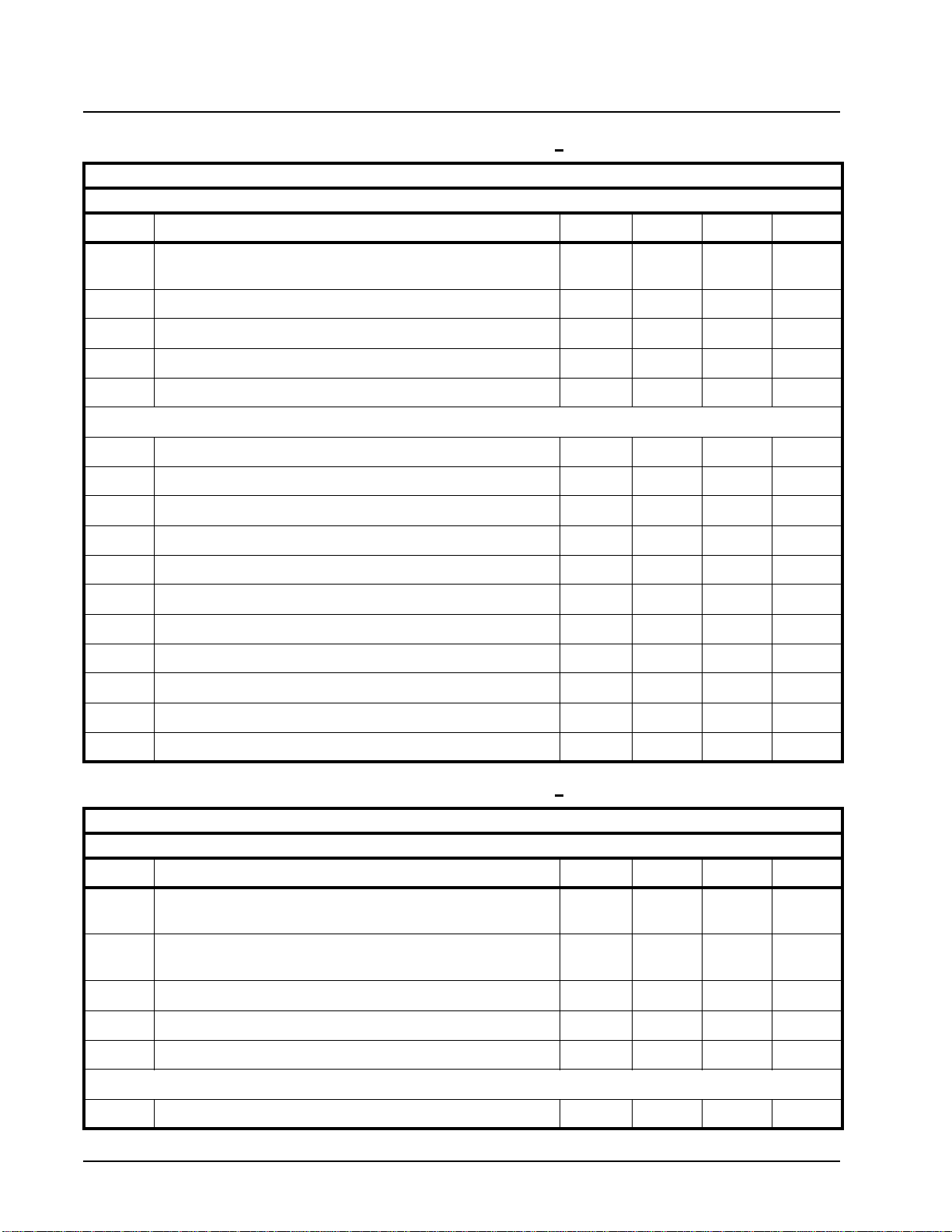
ELECTRICAL CHARACTERISTICS
N
OTE
: * Not applicable to pins with pull-down resistors.
ELECTRICAL CHARACTERISTICS (TA= 25°C, VDD = 3.3V + 5%, UNLESS OTHERWISE SPECIFIED)
SYMBOL PARAMETER MIN.TYP.M
AX.U
NITS
DC Electrical Characteristics
DVDD Digital DC Supply Voltage 3.135 3.3 3.465 V
AVDD Analog DC Supply Voltage 3.135 3.3 3.465 V
ICC Supply Current (Measured while Transmitting and Receiving all
"1’s") 325 370 mA
VIL Input Low Voltage * 0.8 V
VIH Input High Voltage * 2.0 5.0 V
VOL Output Low Voltage, IOUT = -4.0mA * 0.4 V
VOH Output High Voltage, IOUT = 4.0mA * 2.8 V
ILInput Leakage Current * ±10 µA

XRT73L03 áç
áçáç
áç
3 CHANNEL DS3/E3/STS-1 LINE INTERFACE UNIT
REV. 1.1.0
16
N
OTES
:
1. All XRT73L03 digital inputs are designed to be TTL
5V compliant.
2. All XRT73L03 digital outputs are also TTL 5V com-
pliant. However, these outputs will not drive to 5V
nor will they accept external 5V pull-ups.
ELECTRICAL CHARACTERISTICS (CONTINUED) (TA= 25°C, VDD = 3.3V + 5%, UNLESS OTHERWISE SPECIFIED)
AC ELECTRICAL CHARACTERISTICS (SEE FIGURE 5)
TERMINAL SIDE TIMING PARAMETERS (SEE FIGURE 6 AND FIGURE 7) -- {(n) = 0, 1 OR 2 }
SYMBOL PARAMETER MIN.TYP.M
AX.U
NITS
TxClk_(n) Clock Duty Cycle (STS-1/DS3) 30 50 70 %
TxClk_(n) Clock Duty Cycle (E3) 30 50 70 %
TxClk_(n) Frequency (SONET STS-1) 51.84 MHz
TxClk_(n) Frequency (DS3) 44.736 MHz
TxClk_(n) Frequency (E3) 34.368 MHz
tRTX TxClk_(n) Clock Rise Time (10% to 90%) 3 5 ns
tFTX TxClk_(n) Clock Fall Time (90% to 10%) 3 5 ns
tTSU TPData_(n)/TNData_(n) to TxClk_(n) Falling Set up time 3 1.5 ns
tTHO TPData_(n)/TNData_(n) to TxClk_(n) Falling Hold time 3 1.5 ns
tLCVO RxClk_(n) to rising edge of LCV_(n) output delay 2.5 ns
tTDY TTIP_(n)/TRing_(n) to TxClk_(n) Rising Propagation Delay time 8 ns
RxClk_(n) Clock Duty Cycle 50 %
RxClk_(n) Frequency (SONET STS-1) 51.84 MHz
RxClk_(n) Frequency (DS3) 44.736 MHz
RxClk_(n) Frequency (E3) 34.368 MHz
tCO RxClk_(n) to RPOS_(n)/RNEG_(n) Delay Time 0 2.5 ns
tRRX RxClk_(n) Clock Rise Time (10% to 90%) 1.5 ns
tFRX RxClk_(n) Clock Fall Time (10% to 90%) 1.5 ns
CIInput Capacitance 10 pF
CLLoad Capacitance 10 pF

áç
áçáç
áç XRT73L03
3 CHANNEL DS3/E3/STS-1 LINE INTERFACE UNIT
REV. 1.1.0
17
FIGURE 5. TRANSMIT PULSE AMPLITUDE TEST CIRCUIT FOR E3, DS3 AND STS-1 RATES (TYPICAL CHANNEL)
FIGURE 6. TIMING DIAGRAM OF THE TRANSMIT TERMINAL INPUT INTERFACE
R1
31.6Ω
R2
31.6Ω
Channel (n)
Channel (n)
TxPOS_(n)
TxNEG_(n)
TxLineClk_(n)
TTIP_(n)
TRing_(n)
TPData_(n)
TNData_(n)
TxClk_(n)
Only One Channel Shown
1:1
R3
75Ω
TPDATA or
TNDATA
TTIP or
TRING
TClk
t
TSU
t
THO
t
RTX
t
FTX
t
TDY
FIGURE 7. TIMING DIAGRAM OF THE RECEIVE TERMINAL OUTPUT INTERFACE
RClk
t
RRX
t
FRX
RPOS or
RNEG
LCV
t
LCVO
t
CO
XRT73L03 áç
áçáç
áç
3 CHANNEL DS3/E3/STS-1 LINE INTERFACE UNIT
REV. 1.1.0
18
ELECTRICAL CHARACTERISTICS (CONTINUED), (TA= 25°C, VDD = 3.3V + 5%, UNLESS OTHERWISE SPECIFIED)
LINE SIDE PARAMETERS E3 APPLICATION
TRANSMIT CHARACTERISTICS (SEE FIGURE 5)
SYMBOL PARAMETER MIN.T
YP.M
AX UNITS
Transmit Output Pulse Amplitude
(Measured at Secondary Output of Transformer) 0.9 1.0 1.1 Vpk
Transmit Output Pulse Amplitude Ratio 0.95 1.00 1.05
Transmit Output Pulse Width 12.5 14.55 16.5 ns
Transmit Output Pulse Width Ratio 0.95 1.00 1.05
Transmit Output Jitter with jitter-free input @ TxClk_(n) 0.02 0.05 UIpp
Receive Line Characteristics
Receive Sensitivity (Length of cable) 1200 feet
Interference Margin -20 -15 dB
Signal Level to Declare Loss of Signal -35 dB
Signal Level to Clear Loss of Signal -15 dB
Occurrence of LOS to LOS Declaration Time 10 255 UI
Termination of LOS to LOS Clearance Time 10 255 UI
Intrinsic Jitter (As Measured in the RxClk_(n) signal) 0.02 UI
Jitter Tolerance @ Jitter Frequency = 100Hz 64 UI
Jitter Tolerance @ Jitter Frequency = 1kHz 30 UI
Jitter Tolerance @ Jitter Frequency = 10kHz 4 UI
Jitter Tolerance @ Jitter Frequency = 800kHz 0.15 UI
ELECTRICAL CHARACTERISTICS (CONTINUED), (TA= 25°C, VDD = 3.3V + 5%, UNLESS OTHERWISE SPECIFIED)
LINE SIDE PARAMETERS SONET STS-1 APPLICATION
TRANSMIT CHARACTERISTICS (SEE FIGURE 5)
SYMBOL PARAMETER MIN.T
YP.M
AX UNITS
Transmit Output Pulse Amplitude
(Measured with TxLEV=0) 0.68 0.75 0.85 Vpk
Transmit Output Pulse Amplitude
(Measured with TxLEV=1) 0.93 0.98 1.08 Vpk
Transmit Output Pulse Width 8.6 9.65 10.6 ns
Transmit Output Pulse Amplitude Ratio 0.9 1.0 1.1
Transmit Output Jitter with jitter-free input @ TxClk_(n) 0.02 0.05 UI
Receive Line Characteristics
Receive Sensitivity (Length of Cable) 1000 feet
Table of contents
Other Exar Recording Equipment manuals


