FRIENDCOM WSN27-915R User manual

2
This page is blank.

3
WSN27-915(B)R
LICENSE-FREE SOLUTION
For Sub-1G Frequency Band
915 MHz Wi-SUN 6LoWPAN RFModule
1 Overview
WSN27-915(B)R is a RF module compliant with interoperable Wireless Smart Ubiquitous IoT
Network standard as described by IEEE® 802.15.4g/e. It is ideally suited for use as an embedded RF
module in one or two-way data links with electricity meters, DA sensor, devices, terminals and
concentrators.
2BLOCK DIAGRAM
Note: The above block diagram is only used to indicate the internal structure of the module.
Embedded Module

4
3PIN DESCRIPTION
INTERFACE PINS DEFINITION
Pin
Symbol
Name
Definition
1
GND
RF Gnd
Connected to power ground
2
ANT
RF Port
Module RF output, external antenna
3
GND
RF Gnd
Connected to power ground
4
RXD1
Debug UART1
Module debug serial port data receiving end, connecting
user data sending end, RSTTL level, 3.3V
5
TXD1`
Debug UART1
Module debug serial port data sending end, connecting
user data receiving end, RSTTL level, 3.3V
6
RXD0
APP UART0
The module communicates with the data receiving end of
the serial port of the external device and connects with the
user data sending end, with RSTTL level of 3.3V
7
TXD0
APP UART0
The module communicates with the data sending end of
the serial port of the external device and connects with the
user data receiving end, with RSTTL level of 3.3V
8
GND
Power Gnd
External power supply cathode
9
+3.3V
Power supply
External power supply positive pole, voltage 3.3V, power
supply load current at least 1A
10
IOA7
Communication
Indicator
Low level when sending data, external LED indicator
11
IOA6
Communication
Indicator
Low level when receiving data, external LED indicator
12
Boot
Startup control
Start mode selection, internal is pulled down, embedded
flash boot when Boot=0, Boot=1 internal ROM boot,
13
RESET
Reset
Reset RF module at low level
14
IOE4
Communication
Network indication, output low level, external LED indicator

5
Indicator
15
TXD5
IO Port
Expansion port, connecting SRAM HOLD pin of external
equipment
16
RXD5
IO Port
Expansion port, connecting SRAM WP pin of external
equipment
17
MODE
Mode Select
Internal pull-up, MODE=0: Debug mode MODE=1: Normal
mode
18
SWIO
IO Port
Data signal of debug port
19
SWCLK
IOPort
Clock signal of debug port
20
GND
Power Gnd
Connect to power ground
21
TXD4
IO Port
NC, extended standby
22
RXD4
IO Port
NC, extended standby
23
SDA
IO Port
NC, extended standby
24
SCL
IO Port
NC, extended standby
25
SPI_MOSI
IO Port
Connect SPI of external equipment_ MOSI pin
26
SPI_MISO
IO Port
Connect SPI of external equipment_ MISO pin
27
SPI_CLK
IO Port
Connecting SPI of external equipment_ CLK foot
28
SPI_CSN
IO Port
Connecting SPI of external equipment_ CSN pin
29
IOB8
IO Port
SRAM CSN, connect CS pin of external SRAM
30
GND
Power Gnd
Power supply ground
31
+5V
Power Supply
Positive pole of power supply, PA power supply, the load
current of power supply is required to be at least 1A
32
GND
Power Gnd
Power supply ground
4SIZE DESCRIPTION
The specific dimensions of the module are shown in the figure below:

6
5SCHEMATIC DESIGN
At the periphery of RF module, a 1206 packaged magnetic bead M1 and filter capacitor shall be
connected in series to the 5 V power supply interface, and L2, C18 and C19 constitute the antenna
port matching circuit.
5.1
Debug Interface as follows.
5.2
LED indication, plus PSRAM (increase node capacity) schematic diagram is as follows.
5.3
Antenna port
The WSN27-915(B)R communication module is encapsulated by the patch. The user PCB board
should leave an antenna port. The user configures the appropriate antenna according to the actual
application. The antenna port is impedance of 50Ohm and connected to the external antenna of 50
Ohm.
6Antenna Design

7
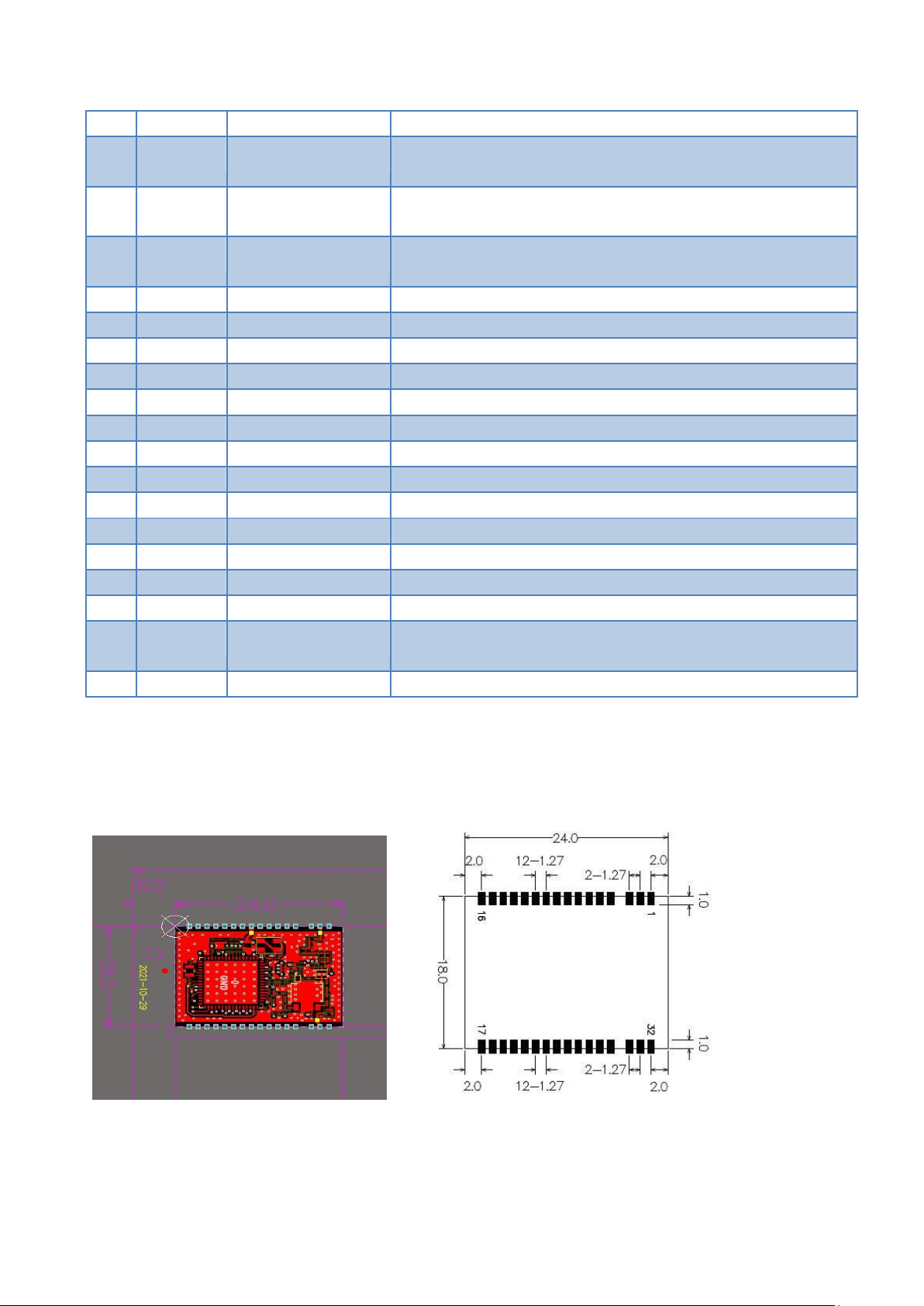
The Wi-SUN RF module is packaged in a stamp hole patch. All I/O ports and antenna ports need to
be led out from the user board. Suggested RF signal routing: PCB Layout RF routing between the
module and the antenna is required to be 50Ω Impedance rule design, and trace length as short as
possible. Since the impedance cannot be controlled, it is recommended that the impedance line
width be 0.8-1mm when routing the PCB Layout, and the distance between the surrounding
grounding copper foil be 1-1.5 times the line width. Ground vias to ensure that the grounding
impedance is as small as possible. Keep the RF port away from all sources of interference, especially
high-speed digital signals and switching power supplies, otherwise the receiving sensitivity of the
module will be reduced.
If a long trace is used, a matching network needs to be added in the middle, as shown in the figure
below.
In order to reduce the reduction of the antenna performance caused by the parasitic capacitor
caused by the RF pad, the first and second layers of the module radio frequency port pads are
recommended to be hollowed out, as shown in the figure below.
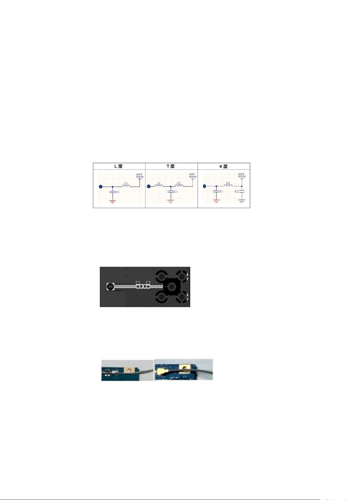
The method of outer radiation frequency feed cable or IPEX welding is connected to the module,
but it is necessary to ensure the sufficientness of the welding and prevent excessive cable damage
from affecting the radio frequency performance of the module. The effect diagram of the two
connection methods is shown in the figure below.
The antenna used in the module must meet the equipment standards. The Bobby should be
between 1.1 and 1.5, the input impedance is 50Ω, the use environment is different, and the gain
requirements for the antenna are also different. Generally, the greater the internal gain, the more
foreign gain, the gain of the external gain, The smaller, the better the antenna performance
Notice: Check the stick external antenna specification for details.

8
7TECHNICAL SPECIFICATION
No.
Parameters Index
Value Description
1
Chip set
Cortex-M3 MCU, 512 KB Flash, 128 KB SRAM, sub-GHz
radio
2
Operating Frequency
902-928MHz
3
Data Modulation
GMSK
4
Operating Mode
RF channel hopping
5
Number of Channels (50 Kbps)
129
6
Interfaces
Application UART & Debug UART,115200-8-n-1
7
Main Host Operating Voltage
3.3V ±10%
8
Radio PA Operating Voltage
5V±10% or 3.3V ±10%
9
RF Receive Current
40mA
10
Operating Temperature Range
-40℃~+70℃
11
Mechanical Dimension
24×18×3 mm
8RADIO SPECIFICATION
Frequency
(MHz)
Wi-SUN PHY
Mode
Data Rate
Modulation
Modulation
Index
No. of
Channels
Channel
Spacing(KHz)
902-928MHz
3
50kbps
2GFSK
1
129
200

9
9FREQUENCY MAPPING
Channel Definitions is as the following table:
No.
Frequency
Center
(MHz)
No.
Frequency
Center
(MHz)
No.
Frequency
Center
(MHz)
No.
Frequency
Center
(MHz)
1
902.2
16
905.2
31
908.2
46
911.2
2
902.4
17
905.4
32
908.4
47
911.4
3
902.6
18
905.6
33
908.6
48
911.6
4
902.8
19
905.8
34
908.8
49
911.8
5
903.0
20
906.0
35
909.0
50
912.0
6
903.2
21
906.2
36
909.2
51
912.2
7
903.4
22
906.4
37
909.4
52
912.4
8
903.6
23
906.6
38
909.6
53
912.6
9
903.8
24
906.8
39
909.8
54
912.8
10
904.0
25
907.0
40
910.0
55
913.0
11
904.2
26
907.2
41
910.2
56
913.2
12
904.4
27
907.4
42
910.4
57
913.4
13
904.6
28
907.6
43
910.6
58
913.6
14
904,8
29
907,8
44
910,8
59
913,8
15
905.0
30
908.0
45
911.0
60
914.0
No.
Frequency
Center
(MHz)
No.
Frequency
Center
(MHz)
No.
Frequency
Center
(MHz)
No.
Frequency
Center
(MHz)
61
914.2
76
917.2
91
920.2
106
923.2
62
914.4
77
917.4
92
920.4
107
923.4
63
914.6
78
917.6
93
920.6
108
923.6
64
914.8
79
917.8
94
920.8
109
923.8
65
915.0
80
918.0
95
921.0
110
924.0
66
915.2
81
918.2
96
921.2
111
924.2
67
915.4
82
918.4
97
921.4
112
924.4
68
915.6
83
918.6
98
921.6
113
924.6
69
915.8
84
918.8
99
921.8
114
924.8
70
916.0
85
919.0
100
922.0
115
925.0
71
916.2
86
919.2
101
922.2
116
925.2
72
916.4
87
919.4
102
922.4
117
925.4
73
916.6
88
919.6
103
922.6
118
925.6
74
916,8
89
919,8
104
922,8
119
925,8
75
917.0
90
920.0
105
923.0
120
926.0

10
No.
Frequency
Center
(MHz)
No.
Frequency
Center
(MHz)
No.
Frequency
Center
(MHz)
No.
Frequency
Center
(MHz)
121
926.2
122
926.4
123
926.6
124
926.8
125
927.0
126
927.2
127
927.4
128
927.6
129
927.8
10 Hopping Scheme
Each module will receive at its channel according to channel order table(Channel1--Channel2
-channels--....Channel 129).If module A transmits RF frame to module B module A first know the
receiving channel of module B.
Channel hopping average interval is 25 S. The maximum time of each transmission is 200ms.
11 TX POWER SPECIFICATION
Power ±1dB
3.3V
5V
20dBm
<150mA
23dBm
<450mA
27dBm
<150mA
<600mA

11
12 RX SENSITIVITY
-108dBm@50Kbps,PER=10%
Shenzhen Friendcom Technology Co.,Ltd.
5th-6th Floor, 17 Building, Guangqian Industrial Park, Xili Town,
Nanshan District, Shenzhen, 518055, China
Tel: +86-755-86026600
Fax: +86-755-86026300

This equipment complies with the FCC RF radiation exposure limits set forth for an uncontrolled environment.
This equipment should be installed and operated with a minimum distance of 20cm between the radiator and any part
of your body.
FCC Statement
This device complies with part 15 of the FCC Rules. Operation is subject to the following two conditions: (1) This device
may not cause harmful interference, and (2) this device must accept any interference received, including interference
that may cause undesired operation.
Any Changes or modifications not expressly approved by the party responsible for compliance could void the user's
authority to operate the equipment.
Note: This equipment has been tested and found to comply with the limits for a Class B digital device, pursuant to part
15 of the FCC Rules. These limits are designed to provide reasonable protection against harmful interference in a
residential installation. This equipment generates, uses and can radiate radio frequency energy and, if not installed and
used in accordance with the instructions, may cause harmful interference to radio communications. However, there is
no guarantee that interference will not occur in a particular installation. If this equipment does cause harmful
interference to radio or television reception, which can be determined by turning the equipment off and on, the user is
encouraged to try to correct the interference by one or more of the following measures:
—Reorient or relocate the receiving antenna.
—Increase the separation between the equipment and receiver.
—Connect the equipment into an outlet on a circuit different from that to which the receiver is connected.
—Consult the dealer or an experienced radio/TV technician for help.
FCC Radiation Exposure Statement
This modular complies with FCC RF radiation exposure limits set forth for an uncontrolled environment. This equipment
should be installed and operated with a minimum distance of 20cm between the radiator and your body.
Shenzhen Friendcom Technology Development Co., Ltd./ADS-BLEnRF1-ANT902 MHz - 928 MHz:
2dBi(declare by Applicant)

Compliance list INTEGRATION INSTRUCTIONS for 996369 D03 OEM the and 996369 D03 OEM by Sections 2.2 through
2.12.
Requirement
Yes
N/A
Comment
2.2 List of applicable FCC rules
List the FCC rules that are applicable to the
modular transmitter. These are the rules that
specifically establish the bands of operation,
the power, spurious emissions, and operating
fundamental frequencies. DO NOT list
compliance to unintentional-radiator rules
(Part 15 Subpart B) since that is not a
condition of a module grant that is extended
to a host manufacturer. See also Section 2.10
below concerning the need to notify host
manufacturers that further testing is
required.3
YES
FCC standards: FCC CFR Title 47 Part 15
Subpart C Section 15.247
2.3 Summarize the specific operational use
conditions
Describe use conditions that are applicable to
the modular transmitter, including for example
any limits on antennas, etc. For example, if
point-to-point antennas are used that require
reduction in power or compensation for cable
loss, then this information must be in the
instructions. If the use condition limitations
extend to professional users, then instructions
must state that this information also extends to
the host manufacturer’s instruction manual. In
addition, certain information may also be
needed, such as peak gain per frequency band
and minimum gain, specifically for master
devices in 5 GHz DFS bands.
YES
Glue stick antenna with antenna gain 2dBi
2.4 Limited module procedures
If a modulartransmitter is approved as a “limited
module,” then the module manufacturer is
responsible for approving the host environment
that the limited module is used with. The
manufacturer of a limited module must describe,
both in the filing and in the installation
instructions, the alternative means that the
limited module manufacturer uses to verify that
the host meets the necessary requirements to
satisfy the module limiting conditions.
A limited module manufacturer has the
flexibility to define its alternative method to
address the conditions that limit the initial
approval, such as: shielding, minimum
N/A
Not applicable

signaling amplitude, buffered modulation/data
inputs, or power supply regulation. The
alternative method could include that the limited
module manufacturer reviews detailed test data
or host designs prior to giving the host
manufacturer approval.
This limited module procedure is also
applicable for RF exposure evaluation when it
is necessary to demonstrate compliance in a
specific host. The module manufacturer must
state how control of the product into which the
modular transmitter will be installed will be
maintained such that full compliance of the
product is always ensured. For additional hosts
other than the specific host originally granted
with a limited module, a Class II permissive
change is required on the module grant to
register the additional host as a specific host
also approved with the module.
2.5 Trace antenna designs
For a modular transmitter with trace antenna
designs, see the guidance in Question 11 of
KDB Publication 996369 D02 FAQ –Modules for
Micro-Strip Antennas and traces. The
integration information shall include for the
TCB review the integration instructions for the
following aspects: layout of trace design, parts
list (BOM), antenna, connectors, and isolation
requirements.4
a) Information that includes permitted
variances (e.g., trace boundary limits, thickness,
length, width, shape(s), dielectric constant, and
impedance as applicable for each type of
antenna);
b) Each design shall be considered a
different type (e.g., antenna length in
multiple(s) of frequency, the wavelength, and
antenna shape (traces in phase) can affect
antenna gain and must be considered);
c) The parameters shall be provided in
a manner permitting host manufacturers to
design the printed circuit (PC) board layout;
d)
Appropriate parts
by
manufacturer and specifications;
e) Test procedures for design verification;
and
N/A
Not applicable

compliance.
The module grantee shall provide a notice that
any deviation(s) from the defined parameters of
the antenna trace, as described by the
instructions, require that the host product
manufacturer must notify the module grantee
that they wish to change the antenna trace
design. In this case, a Class II permissive change
application is required to be filed by the
grantee, or the host manufacturer can take
responsibility through the change in FCC ID
(new application) procedure followed by a Class
II permissive change application.
2.6 RF exposure considerations
It is essential for module grantees to clearly and
explicitly state the RF exposure conditions that
permit a host product manufacturer to use the
module. Two types of instructions are
required for RF exposure information: (1) to the
host product manufacturer, to define the
application conditions (mobile, portable –xx
cm from a person’s body); and (2) additional
text needed for the host product manufacturer
to provide to end users in their end-product
manuals. If RF exposure statements and use
conditions are not provided, then the host
product manufacturer is required to take
responsibility of the module through a change
in FCC ID (new application).
YES
This modular complies with FCC RF radiation
exposure limits set forth for an uncontrolled
environment. This transmitter must not be
co-located or operating in conjunction with
any other antenna or transmitter.
2.7 Antennas
A list of antennas included in the application for
certification must be provided in the instructions.
For modular transmitters approved as limited
modules, all applicable professional installer
instructions must be included as
part of the information to the host product
manufacturer. The antenna list shall also identify
the antenna types (monopole, PIFA, dipole, etc.
(note that for example an “omni-directional
antenna” is not considered to be a specific
“antenna type”)).
For situations where the host product
manufacturer is responsible for an external
connector, for example with an RF pin and
antenna trace design, the integration
instructions shall inform the installer that
YES
Glue stick antenna with antenna gain 2dBi

unique antenna connector must be used on the
Part 15 authorized transmitters used in the host
product. The module manufacturers shall
provide a list of acceptable unique connectors.
2.8 Label and compliance information Grantees
are responsible for the continued compliance of
their modules to the FCC rules. This includes
advising host product manufacturers that they
need to provide a physical or e-label stating
“Contains FCC ID” with their finished product.
YES
If the FCC identification number is not
visible when the module is installed inside
another device, then the outside of the
device into which the module is installed
must also display a label referring to the
enclosed module. This exterior label can
use wording such as the following:
“Contains Transmitter Module FCC ID:
UU3FC-3902-915 Or Contains FCC ID:
UU3FC-3902-915
2.9 Information on test modes and additional
testing requirements5
Additional guidance for testing host products is
given in KDB Publication 996369 D04 Module
Integration Guide. Test modes should take into
consideration different operational conditions
for a stand-alone modular transmitter in a host,
as well as for multiple simultaneously
transmitting modules or other transmitters in a
host product.
The grantee should provide information on how
to configure test modes for host product
evaluation for different operational conditions
for a stand-alone modular transmitter in a host,
versus with multiple, simultaneously
transmitting modules or other transmitters in a
host.
Grantees can increase the utility of their modular
transmitters by providing special means, modes,
or instructions that simulates or characterizes a
connection by enabling a transmitter. This can
greatly simplify a host manufacturer’s
determination that a module as installed in a host
complies with FCC requirements.
YES
The modular transmitter has been fully tested
by the module grantee on the required
number of channels, modulation types, and
modes, it should not be necessary for the host
installer to re-test all the available transmitter
modes or settings.
2.10 Additional testing, Part 15 Subpart B
disclaimer
The grantee should include a statement that
the modular transmitter is only FCC authorized
for the specific rule parts (i.e., FCC transmitter
rules) listed on the grant, and that the host
product manufacturer is responsible
YES
Refer to instruction
Any company of the host device which install this modular
with limit modular approval should perform the test of
radiated & conducted emission and spurious emission,etc.
according to FCC part 15B : 15107 and 15.109, 15B Class B
requirement, Only if the test result comply with FCC part
15B : 15.107 and 15.109, 15B Class B requirement,then the
host can be
sold legally.

for compliance to any other FCC rules that
apply to the host not covered by the modular
transmitter grant of certification. If the grantee
markets their product as being Part 15 Subpart
B compliant (when it also contains
unintentional-radiator digital circuity), then the
grantee shall provide a notice stating that the
final host product still requires Part 15 Subpart
B compliance testing with the modular
transmitter installed.
When the module is installed inside another device, the
user manual of the host must contain below warning
statements;
Note: This equipment has been tested and found to comply
with the limits for a Class B digital device, pursuant to part 15
of the FCC Rules. These limits are designed to provide
reasonable protection against harmful interference in a
residential installation. This equipment generates, uses and
can radiate radio frequency energy and, if not installed and
used in accordance with the instructions, may cause harmful
interference to radio communications.
However, there is no guarantee that interference will not
occur in a particular installation. If this equipment does cause
harmful interference to radio or television reception, which
can be determined by turning the equipment off and on, the
user is encouraged to try to correct the interference by
one or more
of the following measures:
—Reorient or relocate the receiving antenna.
—Increase the separation between the equipment and
receiver.
—Connect the equipment into an outlet on a circuit
different from that to
which the receiver is connected.
—Consult the dealer or an experienced radio/TV technician
for help.
2.11 Note EMI Considerations
Note that a host manufacture is recommended
to use D04 Module Integration Guide
recommending as "best practice" RF design
engineering testing and evaluation in case
non-linear interactions generate additional
non-compliant limits due to module placement
to host components or properties
For standalone mode, reference the guidance in
D04 Module Integration Guide and for
simultaneous mode7; see D02 Module Q&A
Question 12, which permits the host
manufacturer to confirm compliance.
YES
Note: host manufacture is recommended to use D04
Module Integration Guide recommending as "best
practice" RF design engineering testing and evaluation in
case non-linear interactions generate additional
non-compliant limits due to module placement to host
components or properties
For standalone mode, reference the guidance in D04
Module Integration Guide and for simultaneous mode7;
see D02 Module Q&A Question 12, which permits the
host manufacturer to confirm compliance.

2.12 How to make changes
Since . only Grantees are permitted to
make permissive changes, it is
recommended that module manufactures
provide contact information and some
guidance to host providers in the
integration instructions if they expect their
module will be used differently than
granted.
YES
only Grantees are permitted to make
permissive changes.

IC STATEMENT
This device contains licence-exempt transmitter(s)/receiver(s) that comply with Innovation,
Science and Economic
Development Canada’s licence-exempt RSS(s). Operation is subject to the following two
conditions:
(1) This device may not cause interference.
(2) This device must accept any interference, including interference that may cause undesired
operation of the device
Cet appareil contient des émetteurs / récepteurs exemptés de licence conformes aux RSS (RSS)
d'Innovation, Sciences
et Développement économique Canada. Le fonctionnement est soumis aux deux conditions
suivantes :
(1) Cet appareil ne doit pas causer d'interférences.
(2) Cet appareil doit accepter toutes les interférences, y compris celles susceptibles de provoquer
un fonctionnement
indésirable de l'appareil.
IC Radiation Exposure Statement
This modular complies with IC RF radiation exposure limits set forth for an uncontrolled
environment. This transmitter
must not be co-located or operating in conjunction with any other antenna or transmitter.
If the IC number is not visible when the module is installed inside another device, then the
outside of the device into
which the module is installed must also display a label referring to the enclosed module. This
exterior label can
use wording such as the following: “Contains IC: 11418A-BLENRF1”
when the module is installed inside another device, the user manual of this device must contain
below warning
statements;
1. This device contains licence-exempt transmitter(s)/receiver(s) that comply with Innovation,
Science and Economic
Development Canada’s licence-exempt RSS(s). Operation is subject to the following two
conditions:
(1) This device may not cause interference.
(2) This device must accept any interference, including interference that may cause undesired
operation of the device.
2. Cet appareil contient des émetteurs / récepteurs exemptés de licence conformes aux RSS (RSS)
d'Innovation,
Sciences et Développement économique Canada. Le fonctionnement est soumis aux deux
conditions suivantes :
(1) Cet appareil ne doit pas causer d'interférences.
(2) Cet appareil doit accepter toutes les interférences, y compris celles susceptibles de provoquer
un fonctionnement
indésirable de l'appareil.

The devices must be installed and used in strict accordance with the manufacturer's instructions
as described in the user
documentation that comes with the product.
This manual suits for next models
1
Table of contents
Popular Computer Hardware manuals by other brands

Orsys
Orsys micro-line C6713CPU Hardware reference guide

NXP Semiconductors
NXP Semiconductors i.MX 6SoloX SABRE-SDB quick start guide

Texas Instruments
Texas Instruments tideP-0095 Reference design

Fakir
Fakir prestige TV 18 operating instructions

InPOWER
InPOWER 1IPSE1A33-60 Technical documentation

DAQ system
DAQ system ADP-ADI01 user manual