G-QRP Club Limerick Sudden User manual

1
The G-QRP Club
The Limerick Sudden 80m Transmier Kit
Circuit design – Ge rge D bbs G3RJV
PCB design – Rex Harper W1REX
Kit – Graham Firth G3MFJ
Manual – G3RJV and G3MFJ

2
Founded in 1974, the G-QRP Club is the largest QRP Club in the
world. The club e ists to promote interest and growth in low
power amateur radio communication (5 watts or less). Member-
ship is open to any licensed radio amateur or short wave listener
anywhere in the world.
The club publishes a quarterly journal called SPRAT, which is
sent free to members. SPRAT contains many circuits, technical
hints and ideas for QRP construction projects, together with club
news, contest and award information and other items of interest
to QRP operators. SPRAT is an e clusive QRP journal and con-
tains much practical information in each issue. The club operates
a club sales department where components are available at spe-
cial prices to club members. We also publish QRP books which
are available to members.
If you are not a member, and would like to find out more, please
look at www.gqrp.com. For a sample SPRAT and a membership
form, please send your name and address to our membership
secretary:
Daphne Newsum G7ENA, 33 Swallow Drive, Louth, LN11 0DN
membership@gqrp.co.uk
Please mention where you saw this information

3
Transmier Overview
The Limerick Sudden Transmier is a simple circuit f r a reliable QRP transmier. Alt-
h ugh crystal c ntr lled, the scillat r stage (T1) is a Variable Crystal Oscillat r (VXO).
The crystal supplied is a fundamental frequency crystal n 3.560MHz, the QRP calling
frequency n the 80 metre band, alth ugh ther frequencies are available f r the CW
end f this band. N 5ce that an induct r (L1) and a variable capacit r (VC1) have been
added in series with the crystal and gr und. These induc5ve and capaci5ve elements
all w s me shi7ing f the frequency.
The scillat r utput is c upled via C4 t a 2N3904 Driver stage (T2). TR1 f rms the RF
(radi frequency) l ad f r the stage. It is als a c upling transf rmer t drive the p wer
amplifier. The transf rmer is w und n an FT37-43 c re; a ferrite c re f r br adband
c upling. The primary winding is 25 turns f 30 s.w.g. enameled wire. (G ld) The sec-
ndary winding is 5 turns f the red wire w und ver the centre f the primary winding.
The value f the resistance in the emier f T2 determines the am unt f drive available
t T3 and hence the utput p wer f the transmier. A preset p ten5 meter (VR1) is
placed in series with R6 and acts as a DRIVE c ntr l.
The NPN 2N3906 transist r (T4) is used as a Key Switch t key the transmier. This keys
b th the scillat r and the buffer/driver (T1 and T2). In many QRP transmier designs it
is c mm n t leave the scillat r free running and t key later stages. This is because
keying an RF scillat r can result in a “chirpy” CW n te. H wever, T1 is a crystal c n-
tr lled scillat r and n such chirp ccurs. Keying b th stages verc mes the pr blem
f scillat r break-thr ugh when the scillat r is s5ll running in the receive m de.
SW1 is a NET switch that enables the scillat r t run with ut keying the transmier. It
pr vides 12 v lts f r the scillat r and D1 prevents this v ltage reaching T2. This facility
all ws the scillat r t be heard in the receiver s that the VXO signal can be adjusted t
a desired frequency r aligned with a desired sta5 n signal. “NeHng” is standard prac-
5ce when a separate transmier and receiver are being used; it is als called “sp Hng”
in N rth America.
T3 is the transmier p wer amplifier (the Final). This is a simple Class C amplifier biased
by the drive v ltage fr m TR1. The utput l ad is pr vided by L2, an RF ch ke. A zener
di de (ZD1) ffers pr tec5 n f r the utput transist r sh uld the transmier be inad-
vertently perated with ut an antenna r int a sh rt circuit. A clip- n heat sink keeps
the transist r c l. C6 c uples the RF utput t a seven element L w-Pass Filter based
n the W3NQN filter data, with enhanced 2
nd harm nic filtering.
The capacit r C7 leads t the transmier-receiver break-in circuit p pularized by W7EL
in his “Op5mised Transceiver” design. It is a simple meth d f sharing the same anten-
na by a transmier and receiver with ut damage t the receiver during transmissi n r
significant l ss f signal fr m the transmier. S me mu5ng f the signal fed t the re-
ceiver is achieved by the circuit T5, T6 and T7. The mu5ng circuit is such that when a
receiver is c nnected t the transmier, 12 v lts must be c nnected t the transmier
t hear signals. The mu5ng is m st effec5ve when the c vers are n the transmier and
receiver.

4
Building the Transmier
Y u will have n 5ced that this is a rather unusual kit. It has a printed circuit b ard
with ut any h les. We call it “Limerick C nstruc5 n” because it was designed by Rex
Harper, W1REX, f Limerick, Maine. It is a surface m unted b ard in that the c mp -
nents are m unted n the surface f the b ard, alth ugh the c mp nents used are
“thr ugh-h le” parts. This all ws f r ease f c nstruc5 n and easy c rrec5 n f any
err rs. The main b ard als has the fr nt and back panels f r the transmier. They are
sc red and can be snapped ff the main b ard. We suggest y u sm th the snapped
ff edges with emery paper r an emery b ard. The c mp nent parts are s ldered t
the t p surface f the b ard using the leads that w uld g thr ugh the b ard n a
c nven5 nal printed circuit b ard. The interc nnec5 ns between the m un5ng pads
are ready made but hidden by the black screen printed verlay. The designa5 n f all
the parts is printed next t the appr priate pads. Each sec5 n f the transmier
(OSCILLATOR, DRIVER, FINAL, LOW-PASS FILTER and KEY SWITCH) is als marked n
the b ard. The MUTE circuit c mp nents are m unted n the back panel. Any refer-
ences t t p, b m, le4 and right assume that the b ard is held with the printed text
the c rrect way, with the G-QRP Club l g in the centre right. T p is actually the Rear
f the finished b ard, and b m is, f c urse, the Fr nt.
It d es help t set ut all the c mp nents in the rder
f designa5 n. i.e. C1, C2 etc. The best way is t use a
small piece f p lystyrene t h ld the individual parts.
If y u are g ing t use this idea f r semic nduct rs, a
piece f aluminium f il wrapped r und the p lystyrene
will prevent any sta5c damage. D uble check the ca-
pacit r values—there is a l t f difference between a
101 and a 104 capacit r!
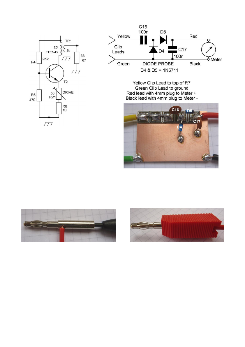
The building f the transmier d es entail winding f ur
c ils n t r id c res (TR1, and L4, L5 and L6), and an RF
ch ke f r the PA wired n a pig-n sed bin cular c re
(L2). The c res are the small rings that l k like miniature “P l Mints”. L1 and L3 are
pre-w und ch kes (c ils) that l k like fat resist rs. Winding the c ils is n t difficult; it
just requires a lile care and the accurate c un5ng f the number f turns. There is
ample guidance in the pages f this manual. It is a g d idea t wind TR1 bef re begin-
ning t add any ther c mp nents t the b ard. It is the m st difficult f the hand-
w und c ils as it has tw windings, a tuned winding and a smaller link winding.
TR1 is w und n the FT37-43 c re. This is the black c re - the ne with ut the yell w
c a5ng. The primary winding has 25 turns f the g ld wire. There is guide as t h w
t wind these n the next page. Each 5me the wire passes thr ugh the h le f the c re
c unts as ne turn. The turns sh uld be laid side by side and ccupy ab ut three-
quarters f the circumference f the c re. The link winding is 5 turns f the red wire
w und ver the centre f the main winding. Placement f the link winding is n t t
cri5cal – just guess the centre p si5 n.

5
When the windings have been made, trim the ends f the wires t ab ut 1cm. The wire is
c ated with enamel insula5 n. Ab ut 5mm f each wire sh uld be 5nned with s lder pri r
t making the c nnec5 ns. The enamel c a5ng n the wire supplied is designed t melt
when the s ldering ir n is applied. This d es require quite a bit f heat. The best meth d is
t f rm a bl b f s lder n the s ldering ir n 5p. Apply the 5p t the very end f the wire
and wait un5l the enamel melts and the s lder fl ws nt the c pper wire. This can take up
t 20 sec nds. Then m ve the wire thr ugh the bl b un5l y u get the required 5mm r s
5nned. It’s best n t t breathe in the sm ke given ff during this pr cess.
Winding t r idal c ils is easy. It just requires pa5ence
and care. TR1 uses the black c re with the g ld wire f r
the main winding. The 25 turns require 15” f wire. Each
5me the wire passes thr ugh the
h le (including the first 5me) it
c unts as ONE turn. H ld the
c re firmly with ne hand and
thread the wire thr ugh
with the ther hand, lay-
ing the windings side by
side. Tighten the wire a7er each turn f r a neat c il.
S me5mes if the wire
gets twisted and f rms
a l p it results in a
kink. Untwist the wire carefully. Trying t pull ut the
kink can snap the wire. C mplete the 25 turns. They
sh uld ccupy ab ut three-quarters f the circumfer-
ence. The 5 turn link winding, using red wire, is added
ver the centre f the main winding. Guess the cen-
tre, it is n t really cri5cal

6
TR1 is m unted ver5cally in the centre f f ur pads. The primary
(larger) winding is s ldered t the t p right pad and the b m
le7 pad. The link (5 turn) winding t the ther tw pads.
The transmier is built in tw sec5 ns; the first being the le7-
hand side f the circuit diagram as far as R7. This includes the
OSCILLATOR, the DRIVER and the KEY SWITCH. These are then
tested bef re the rest f the stages are added.
Begin by s ldering the transist rs T1, T2 and T4 t the appr priate pads.
The shape f the transist rs marked n the b ard indicates their rienta-
5 n. They must be placed the c rrect way r und. T enable a secure s l-
der c nnec5 n f the parts, the leads are bent int an “L” shape f r adding
t the pads n the b ard.
Add the resist rs as far as R9 and the capacit rs C1 t C5,
C8 and C9, C10 and C11. Capacit r C11 is an electr ly5c
capacit r and must be c nnected the c rrect way r und.
The nega5ve lead (marked with a series f dashes – see
drawing) g es t the b m pad f the tw pads designat-
ed f r C11. C8 sh uld be bent t be flat against the b ard as therwise it may f ul the key
jack later.
When the resist rs and capacit rs are in place, the s cket f r X1 (the
quartz crystal), L1, D1 and RV1 sh uld be added in their appr priate
places. The s cket f r X1 is a 3 way strip and alth ugh we nly use
the uter 2 pins, we will c nnect all three pins t the pads n the
circuit b ard. The di de D1 pads have a bar marking t c rresp nd
with the band n the di de. This di de is very similar t ZD1 – y u
may need a magnifying glass t be sure that y u have the c rrect
di de.
The fr nt panel
The fr nt panel h lds the variable tuning capacit r (TUNE), the net switch (NET SW) and
the key jack s cket (KEY). These sh uld be fied, and we suggest that the wiring f r these is
added as well. S lder these at the c mp nent ends first, we will s lder the main b ard
ends later.
The tuning capacit r
The tuning capacit r is a tw sec5 n p lyvaric n type but nly the
sec5 n with the smallest capacitance is used. There are markings
(rather small) t indicate the capacitance f each sec5 n. A = 140pF,
O = 60pF and G = Gr und. We nly require the O and G c nnec5 ns.
The “A” s lder tag can be cut sh rt (but n t rem ved) t av id c n-
fusi n. 2 ff 3cm lengths f wire (yell w (O) and black (G)) f r the
tuning capacit r sh uld be s ldered n the capacit r.
The tuning capacit r is m unted t the fr nt panel using the tw
small screws pr vided. It is m unted tags d wnward.

7
The key jack s cket
The s cket is a 3.5mm s cket t be used with a 3.5mm m n jack plug
s ne f the c nnec5 ns, (which is a switch c ntact), is unused. It is a
g d idea t cut ff the unwanted s lder tag t av id c nfusi n. The
gr und tag sh uld be t the uter edge. The wires f r this will be s l-
dered t the main b ard first, and c nnected t the jack a7er the panel
is fied.
The NET switch
NET SW is a small t ggle switch that requires tw wires
t be j ined t the SW1 pads n the main b ard. Which
wire g es t which pad is n t imp rtant as this is a sim-
ple n/ ff switch. Use the t p tw c ntacts n the
switch f r the wires. When the switch lever is p in5ng
d wnwards a c nnec5 n is made between these tw c ntacts. The n rmal p si5 n f the lever
when using the transmier is upwards. 2 pieces f wire (blue and range, 10 cm l ng) sh uld be
s ldered t the net switch, and then twisted t gether ver their full length. N rth American
builders wh seem t like their switches upside d wn c mpared t Eur pean switches may wish
t use this switch with VFO n being up!
N w, the LED (light emiHng di de) can be m unted n the fr nt
panel. This fits int a small h le marked “SIG” f r signal because the
di de t there t gl w whenever a signal is being transmied.
On the inside f the fr nt panel, either side f the SIG h le, there is a d uble pad and a single
pad. The nega5ve side (-) f the LED is c nnected t gr und at the single pad. The p si5ve side
f the LED is c nnected t the d uble pad nearest the h le. The uter pad, marked “LED” is
c nnected with a wire t the LED pads t the right f R10 n the main b ard. The l ngest lead
f the LED is the p si5ve lead. T m unt the LED, push it int the SIG h le and, using p inted
pliers, gently bend the leads in an arc t reach the desired pads.
The finished fr nt panel sh uld l k like this –
N w rem ve the insula5 n c mpletely fr m tw 2cm
pieces f the black wire, and s lder ne end f each
piece f bare wire t the KEY pads n the main b ard. Be
careful y u d n’t catch y ur fingers n these when they
are stuck up in the air!

8
Add the side cheeks
This is a g d 5me t s lder the “side
cheeks” int place either side f the main
b ard. These are designed as fixing plate f r
the encl sure. Adding the side cheeks at
this p int d es mean that the fixing f the fr nt and back panels f the receiver is much
easier. Aaching the side cheeks d es require a really h t s ldering ir n bit and plenty f
s lder. These are n t iden5cal s make sure y u have the right nes at the c rrect sides –
see the picture bel w t check. We sh uld, at this p int, rec mmend ur SBSS clamps,
which are designed f r this purp se - b th the side cheeks, and the fr nt panel are easily
fixed this way.
If y u d n’t use ur clamps, then we suggest that y u begin with a large bl b f s lder at
ne end t fix the p si5 n. Aempt t get the side cheek as near ver5cal as p ssible and
exactly in line with the main b ard. When y u are happy with this, y u sh uld put a few
bl bs al ng the narr w pads n the length f the b ard. Be careful near the blue variable
resist r, the plas5c easily melts when t uched by the ir n!
When y u have fied these, the fr nt panel can be s ldered
in place – a7er c nnec5ng the variable capacit r and net
switch leads. The O (yell w) g es t the le7-hand pad nearest
t the centre f the fr nt f the b ard, and the G c nnec5 n
(black) g es t the right-hand (nearer the edge) pad.
This picture sh ws that d ne, and the c rrect way r und f
the side panels alth ugh they have n t been s ldered int
place yet.
Like the side cheeks the fr nt panel is
s ldered t the main b ard. This panel,
unlike the side cheeks, verlaps the base
b ard. The base b ard sh uld be put in
the gap between the s ldered tracks at
the b m f the fr nt panel. This pic-
ture sh ws the c rrect p si5 n f the
fr nt panel against the base. Again, we
suggest that y u use the “ ne bl b” tech-
nique underneath the b ard t get the
panel aligned c rrectly and ver5cal. Add a
sec nd bl b when y u are happy with the
alignment, then y u sh uld put a few
g d bl bs f s lder al ng the t p side f the b ard f r extra
strength.
Finally f r this stage, c nnect the tw bare wires t the key
jack – this picture sh ws that d ne. The gr und c nnec5 n
(see diagram—t p f page 7) sh uld be nearest the side f
the case

9
C mplete circuit
diagram

10
Tes9ng the first sec9 n
Tes5ng the transmier at this stage re-
quires a Di de Pr be. All the parts are
pr vided f r making such a pr be as
sh wn in the picture.
The di de pr be is built “Manhaan-style”
by aaching a strip f five pads t the t p
le7-hand c rner f the printed circuit b ard material using super glue. The c mp nents are
surface m unted as sh wn. The three le7-hand pads are j ined using an ff-cut fr m ne f
the trimmed c mp nent leads.
Flexible wire in red, black, yell w and green is supplied. The yell w and green leads are
terminated with cr c dile clips and the red and black leads are terminated with 4mm plugs
(the standard plug used in test meters). If y ur meter uses a different size f plug, then y u
will have t btain these y urself. The placement f the f ur leads is sh wn in the circuit
drawing. Later the di de pr be will be c nverted int a basic wameter t measure the final
transmier utput.
F r th se n t familiar with 4mm plugs, the centre f the metal insert c ntains a grub screw
t secure the end f the wire. A small screw driver pushed up the centre f the metal insert
is used t clamp the end f the wire as sh wn. The metal insert is then pushed int the plas-
5c h using f the plug, wire being place in line with the sl t in the plas5c h using. The insert
is n w pushed un5l the end f the plug is as far ut as it will travel. This d es take f rce!
Pushing the end f the insert against a firm surface will help. Y u might need a screwdriver
t push in the final bit f the metal insert.

11
The cr c dile clips are easier t aach t the ends f the yell w and green wire. Prize the
clip pen a lile and slide ff the plas5c c v-
ering. The wire can be s ldered t the clip
and held in place by the crimps at the end.
Remember – Push the plas5c c vering nt
the wire bef re s ldering the wire in place.
The clip is chr mium plated and s ldering will
be much easier if the area t take the s lder
is r ughed a lile with emery paper r the
edge f a sharp knife.
The red and black leads are plugged int the p si5ve (+) and nega5ve (-) inputs f the meter.
The yell w lead is clipped n the le7 side f R7 (the pad c nnected t the utput f TR1) and
the green lead is c nnected t the ther (gr unded) end f R7. The meter sh uld be set n a
range that will indicate 10 v lts DC.
Tes9ng the Transmier
Having made the RF pr be, the first sec5 n f the transmier is n w ready f r tes5ng, s
make a temp rary supply lead using red & black wires – t the +12 and gr und pads, respec-
5vely, in the centre f the b ard. We suggest that y u make these ab ut 20cm l ng. As a
precau5 n, y u sh uld turn the blue drive preset fully an5-cl ckwise bef re y u p wer the
b ard – d n’t f rget t insert the crystal!
When y u are happy with all the c nnec5 ns (a check that all the parts are in the c rrect
places is useful at this stage). Apply 12 V lt p wer t the b ard: +12v t the red wire, and
the nega5ve t the black wire.
Firstly, check the scillat r. If y u press the net switch, the scillat r nly will run, and this
can be f und ar und 3.560MHz n a suitable receiver. The tune c ntr l sh uld vary the fre-
quency fr m ar und 3.558MHz t 3.561MHz.
[NOTE – there is sc pe f r experiment with the value f the series induct r L1.
Increasing the value f this will give an increase in frequency range, h wever, this
may be at the expense f scillat r stability. The value supplied with the kit is a
safe value. See the m difica5 n n tes n page 17]
Sec ndly, check the keying and driver stages.
A 3.5mm m n jack plug is supplied with the kit t fit
the KEY jack s cket. Aach this t a M rse key r tw
pieces f wire that can be sh rted t simulate a M rse
key.
Depressing the key r j ining the wires sh uld give an indica5 n f a few v lts in the meter
c nnected t the RF pr be. The Oscillat r, Driver and Key Switch stages are all w rking if the
meter sh ws an utput v ltage. Ar und 3 v lts is a reas nable value, and y u sh uld be able
t change this with the drive preset. Remember t turn this back t the fully an5-cl ckwise
p si5 n bef re y u m ve n t the next step.

12
N w, the rest f the transmier.
The final amplifier
Firstly, wind the c il L2. This is 5 turns n a FT43-2402 bin cular
t r id. Each turn g es thr ugh b th h les f the c re, and y u
sh uld end up with it l king like this.
It is helpful t insert this and the ther c mp nents in the sec5 n marked “FINAL” (ZD1,
R10, C6 and C7) bef re adding the final amplifier transist r (T3) (2N3866). ZD1 must be
c nnected the c rrect way r und. The b m pad f the ZD1 placement sh ws a bar
marking; this c rresp nds t the bar ( r ring) near ne end f the zener di de.
Trim the transist r leads t ab ut 10mm and bend the end 3mm f the transist r leads t
f rm a “f t” that will lay flush with the pads. The best direc5 ns f r the f t, assuming
the tab n the transist r case p ints upwards, are emier upwards, c llect r d wnwards
and base t the le7. Refer t the base c nnec5 n diagram n the circuit schema5c. Using
p inted pliers manipulate the leads un5l each f t rests n the required pad. Tin the pads
and the leads and s lder them in place. The heatsink is applied t the transist r by placing
a screwdriver blade in the gap and twis5ng it t pen the vanes. The heatsink sh uld n w
fit ver the transist r casing. The screwdriver is rem ved t all w the heatsink t clamp
firmly n the sides f the transist r.
The next step is t s lder a 10cm length f yell w wire t the LED pad n the main b ard
(just t the rear f the +12v p wer pad, c nnect the ther end f this t the LED pad n
the fr nt panel. Tuck this wire in 5dily as y u can see n the picture f the main b ard and
fr nt panel bel w. The di des D2 & D3 sh uld be s ldered int place - the di de D2/3 pads
have a bar marking (like ZD1) t sh w the way t m unt them. Finally s lder the “fat resis-
t r” sized induct r, L3 int place.
The l w-pass filter
The l w-pass filter c ils (L4, L5 & L6) are w und n the red c res
using the g ld wire. L4 and L6 have 26 turns, L5 has 25 turns. These
require 18” (45cm) f wire f r each c il. Wind as f r TR1 with ne
pass thr ugh the c re being ne turn. L5 has ne less turn (25) than
L4 and L6 (26 each) s wind L5 first and lay it aside s that it w n’t
be c nfused with the thers. 45cm f wire is easily en ugh f r each
c il. The windings n each c re sh uld ccupy ab ut three-quarters
f the circumference.

13
Quite a few f the capacit rs ar und the PA transist r are actually tw in
parallel as the c rrect values are n t c mmercially available. We suggest
that y u parallel these pairs first as sh wn here, bef re fiHng them. A
g d plan is t m unt C12 - C15 and C18, then m unt L5, f ll wed by L4
and L6.
Here is a picture f the c mpleted
b ard s far.
The lay ut f the printed circuit
b ard. This sh ws the wiring between the pads

14
The back panel.
Firstly, m unt the three s ckets n the back panel – the antenna s cket, the receiver aerial
s cket and the p wer s cket.
The antenna s ckets
The antenna s cket (ANT) is a single h le fixing
ph n s cket, as is the RECEIVER s cket. These
require tw wires t be j ined t the ANT pads n
the main b ard and we will c nnect these in a
m ment.
The p wer s cket
The POWER s cket als has tw c nnec5 ns that c nnect t the
main b ard and it is vital t get these the c rrect way r und. Again,
we will c nnect these sh rtly.
The receiver mu9ng
The c mp nents f r the receiver mu5ng sec5 n are m unted inside the back panel, and
y u sh uld n w fit these. S lder the resist rs int place first, f ll wed by the transist rs. It
is best t keep the lead length f these parts sh rt if p ssible.
The next j b is t c nnect the rear panel t main b ard. Firstly, y u need t cut seven
lengths f wire. The first three are n the back panel and are as f ll ws:
RCVR n the back panel c nnects t the centre f the RECEIVER ph n s cket – use
3cm f range wire f r this.
GND n the back panel c nnects t the gr und tag n the RECEIVER ph n s cket –
use 1½cm f bare wire f r this.
S lder a 10cm length f red wire t the +12 tag n the back panel but d n t c nnect
the ther end yet.
N w cut the ther f ur pieces as f ll ws and s lder these t the pads n the main b ard:
R-MUTE n the main b ard – use a 9cm length f green wire f r this.
K-MUTE n the (b m f club l g ) n the main b ard – use a 10cm length f r-
ange wire f r this.
ANT n the main b ard – use tw 9cm lengths f wire – black and blue, the black
(gr und) c nnec5 n g es t the le7-hand pad and the blue (antenna c nnec-
5 n) g es t the right-hand pad. Y
Y u sh uld already have tw pieces f wire c nnected t the +12V and GND tags f
the main b ard that we used f r tes5ng. Cut these t 9cm l ng.

15
Wiring the back panel t the main b ard.
N w, if y u place the rear panel behind the main b ard, y u can c nnect the ther end f
all the wires – green t R-MUTE, range t K-MUTE, black t the uter s lder tag f the
antenna s cket, and the blue wire t the centre c nnec5 n. Finally a7er stripping the ends
f the tw red wires, twist them t gether and s lder them b th t the centre pin f the
p wer s cket.
This picture sh ws that d ne. (N te—this picture is f a 30m transmier s s me c mp -
nents may be different t the 80m TX.)
Finally, having finished the wiring t the back panel, y u sh uld s lder the back panel in
place using the same meth d that y u used f r the fr nt panel. Be careful when s ldering
near the wires as the insula5 n is easily damaged by the s ldering ir n. There is en ugh
length t m ve them ut f the way f the ir n.
Tes9ng the transmier
The first step is t c nvert the RF Pr be int a simple RF
Wameter.
The riginal di de pr be has three 150 Ohm large resis-
t rs added t the three le7-hand pads and gr und.
These resist rs c nnected in parallel f rm a 50 Ohm l ad
f r the transmier. D n t aempt t transmit with ut
either a 50 Ohm l ad r c nnec5ng the utput t a
matched antenna.

16
C nnect the yell w clip lead t the centre f the ANT s cket and the green clip t the gr und
f the ANT s cket and the red and black leads t a v ltmeter. C nnect the 12 v lt supply, leav-
ing the NET SW switch upwards, and press the M rse KEY d wn. Read the utput v ltage. The
v ltage is the peak t peak measure-
ment. If y u are g ing t use the RF wa-
meter 7en, then we suggest that y u
replace the yell w and green leads with
a sh r5sh piece f 50 Ohm c ax termi-
nated in a Ph n (RCA) plug. The inner
c nduct r sh uld g where the yell w
lead was c nnected, and the screen t the c pper where the green wire was c nnected.
The utput in was = r.m.s v ltage
2 divide by 50.
The calcula5 n is simple:
• V ltage reading (peak t peak) divide by 2 = the peak v ltage
• The peak v ltage is mul5plied by 0.707 = the r.m.s. v ltage.
• The r.m.s. v ltage mul5plied by itself = r.m.s. v ltage
2
• Divide this by 50 (the l ad resist r value) f r the RF p wer utput in was.
A suitable 2.1mm p wer plug is supplied with the kit – the centre pin is +ve and the uter c n-
nec5 n is –ve. D n t get these reversed as there is n reverse p larity pr tec5 n in the trans-
mier.
The transmier sh uld pr duce ab ut 1 t 2 was. The Drive c ntr l (RV1) may be used t
adjust the final utput. Alth ugh the 2N3866 final amplifier transist r is quite rugged and is
pr tected by ZD1, it is p ssible t destr y the transist r by either verdriving it, r by trans-
miHng f r m re than a few sec nds int an inc rrect l ad. With this in mind a spare 2N3866
is pr vided with the kit – d n t destr y this as well! We suggest y u begin bel w 1 wa and
increase the utput if y u can, t ar und 2 was maximum. Try f r an utput v ltage n the
test meter f s me 15 t 25 v lts. Tw was n 80 metres represents a useful am unt f QRP
transmier p wer. If y u turn up the drive c ntr l up t much, the utput p wer will start t
g d wn - and this sh uld be av ided as it will pr duce a bad utput signal. Remember t use
the transmier with the NET SW in the upward ( ff) p si5 n. Pressing the switch d wnwards
switches p wer t the scillat r nly. Use this p si5 n t find the frequency f the transmier
n the receiver. This may be used t find a par5cular frequency r t “net” the transmier t
an ther sta5 n. The transmier utput is 50 Ohms and the transmier sh uld be used int a
50 Ohm antenna (e.g. a dip le) r via an Antenna Tuner t match the 50 Ohms t the antenna.

17
Finally – the case
The case parts sh uld n w be s ldered t gether – the imp rtant p int here is that the sides
must be at right-angles t the t p. Again, use the single bl b technique un5l y u are sa5s-
fied with the angles – it is beer if y u d n t s lder right up t the fr nt f the lid as the
case verlaps the fr nt t give a h ded effect, and if y u s lder right up t the fr nt, the
case may n t fit as well.
What next? - P ssibili9es f r experiment
Radi amateurs w uld n t be radi amateurs if they didn't want t experiment with things,
s here are a c uple f things that y u may wish t experiment with. Rem ve the trans-
mier p wer, and be careful that y u d n t destr y anything in the transmier whilst y u
are changing parts! If y u are n t sure f y ur wn abili5es, then ask a m re experienced
c nstruct r t d it f r y u.
The VXO
The VXO circuit is a “sure fire” circuit that will always w rk, but there is a p ssibility t in-
crease the shi7 range by altering the value f L3. If y u increase L3 , then the p lyvaric n
VC1 will m ve the frequency m re. P ssible disadvantages are that either the scillat r will
st p scilla5ng at s me parts f the tuning c ntr l travel, and/ r, the scillat r will chirp
when the TX is keyed. Y u may need the use f the sta5 n receiver t test these. Y u will
pr bably have t unfasten VC1 and m ve it aside t change any f these parts. The p lyvar-
ic n has a sec nd part—this has a capacitance shi7 f 6 t 160pF. Y u may wish t try
swapping the tw parts. When y u have altered any values, take a careful list n a g d
receiver t ensure that y u have a stable n n-chirping transmissi n. Be careful! An ther
change is that y u c uld try tw iden5cal crystals in parallel—this can c nsiderably increase
the VXO shi7
The RX mu9ng circuit
This circuit is a simple and reas nably effec5ve way f c nsiderably reducing the am unt f
transmied signal that gets back t the receiver. Because it is a simple circuit, and there is
n “mute” signal d wn a separate wire t the receiver, then the mu5ng may appear t n t
be w rking very well. In fact, with ut it, the received signal fr m the TX w uld be c nsider-
ably l uder. This is an ther p int at which y u c uld d s me experimen5ng and that is by
replacing C7 with a smaller fixed capacit r in parallel with a trimmer. There is just r m t
d this—but y u will have t be very careful with the s ldering ir n, and av id t uching
nearby parts. Aim, with the tw capacit rs, f r a value when the trimmer is mid-p si5 n, t
be a value ar und the supplied (and n w rem ved) C7. The trimmer sh uld be adjusted
with the TX p wered up, but n t transmiHng. Adjust the trimmer f r the maximum re-
ceived signal strength f a weak signal n the receiver - the weaker the beer. It sh uld n t
be adjusted when y u are either neHng, r transmiHng.
Again - be very careful - this is a m difica5 n f r experience c nstruct rs nly.
We d n t rec mmend that y u t uch r alter parts in the utput f the PA. If y u change
anything, then y u may reduce the harm nic filtering and then there c uld be unwanted r
even illegal radia5 ns fr m the transmier.

18
Value Markings
Resistors
R1 47k Yellow, purple, orange, gold
R2 470 Yellow, purple, brown, gold
R3 120 Brown, red, black, black, brown
R4 2k2 Red, red, red, gold
R5 470 Yellow, purple, brown, gold
R6 10 Brown, black, black, gold
R7 33 Orange, orange, black, gold
R8 1k Brown, black, red, gold
R9 47k Yellow, purple, orange, gold
R10 1k Brown, black, red, gold
R11 2k2 Red, red, red, gold
R12 10k Brown, black, orange, gold
R13 10k Brown, black, orange, gold
R14 150 Brown, green, black, black, brown
R15 150 Brown, green, black, black, brown
R16 150 Brown, green, black, black, brown
Capacitors
C1 100n 104
C2 180p 181
C3 100p 101
C4 47p 47
C5 100n 104
C6 100n 104
C7 94p (47 + 47p )* 47 + 47
C8 100n 104
C9 100n 104
C10 100n 104
C11 10u 10u (the –ve side is plainly marked)
C12 780p (390 + 390p ) * 391 + 391
C13 1300p (1200 + 100p ) * 122 + 101
C14 1300p (1200 + 100p ) * 122 + 101
C15 860p (470 + 390p ) * 471 + 391
C16 100n 104 (for R probe)
C18 197p (150 + 47p ) * 151 + 47
* these values are 2 capacitors in parallel – see text
Inductors
L1 39uH Orange, white, black, silver
L2 BN43-2402 binocular core Pig nose – 5 complete turns 30SWG
L3 22uH Red. red, black, silver
L4 T37-2 Red/black – 26 turns
L5 T37-2 Red/black – 25 turns
L6 T37-2 Red/black – 26 turns
TR1 T37-43 Black – 25t (30SWG) + 5t (27SWG)
C17 100n 104 (for R probe)

19
Other parts
RV1 50 Ohm Drive control preset
VC1 60p Tuning
SW miniature toggle switch Net switch (may be a 2 tag part)
J1 3.5mm mono jack socket Key jack
J2 Phono/RCA socket Antenna
J3 Phono/RCA socket Antenna to receiver
X1 Crystal 7.030MHz HC49U wire lead crystal
Socket Crystal socket 3 SIL sockets
35mm knob or VXO tuning capacitor
Magnet wire 30 SWG Gold coloured
Magnet wire 27 SWG Red coloured
PVC wire 6 colours of wire Red, Black, Orange, Yellow, Blue & Green
Heatsink or PA transistor
Power socket Panel mounting 2.1mm
Power plug 2.1mm
4 feet for case
Key plug 3.5mm mono plug
Blank PCB or probe
5 MEsquares or probe
Extra flexible wire or probe Black, Red, Yellow, Green
4mm plugs or probe Black, Red
Min crocodile clips or probe Yellow, Green
LED Output indicator
ZD1 33v zener diode (BZX55C33) PA protector
D2 1N5711 RX parallel mute
D3 1N5711 RX parallel mute
D4 1N5711 Probe detector
D5 1N5711 Probe detector
D1 1N4148 or net switch
T7 2N7000 RX parallel mute
Semiconductors
T1 2N3904 Oscillator
T2 2N3904 Driver
T3 2N3866 (4-247 CG9949) PA (spare included)
T5 2N7000 RX series mute
T6 2N7000 voltage inverter
T4 2N3906 Keyer
Toroid or T1 T37-43 - black
Toroids or L4, L5 & L6 3 x T37-2 - red/black
Pig-nose toroid or L2 BN43-2402
Screws 4 x self tapping screws To fasten the case on

20
The finished transmier
(NB - This is the 30m versi n f the kit s s me parts will be slightly different)
© G-QRP Club 2010/11/12/13/14/15/16
V2.6 May 2016
Other manuals for Limerick Sudden
1
Other G-QRP Club Transmitter manuals