Phone: +49 371 33 77 - 0
Fax:: +49 371 33 77 272
Internet: www.gemac-chemnitz.de
Email: interpolation@gemac-chemnitz.de
Gesellschaft für
Mikroelektronikanwendung Chemnitz mbH
Zwickauer Straße 227
D-09116 Chemnitz, Germany Date: 25.05.05 Page 7 of 13
Title:
User manual - IPE1000-U
Name of Document:
46500-HB-1-4-E-IPE1000-U.pdf
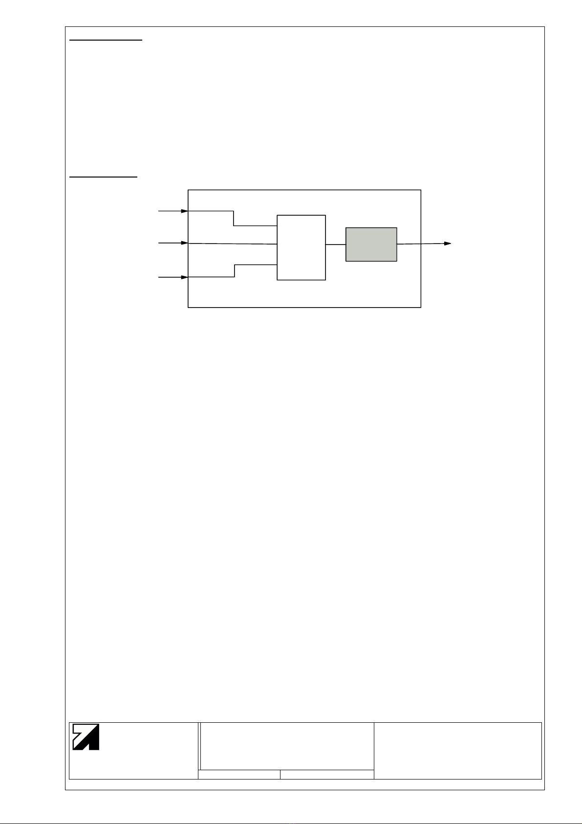
4 Output Signals
4.1 Output Signals RS422
The output signals are phase shifted square wave sequences (known by incremental measuring
transducers). They can be counted in a single or quadruple way. A synchronous reference pulse will be
generated when the angle of 0° (refer also to Fig. 3) is passed through and when the analogue differential
input voltage between REFP and REFN exceeds the positive comparator hysteresis level. If the differential
input voltage is permanently above this level, the reference pulse will be generated once during every signal
period.
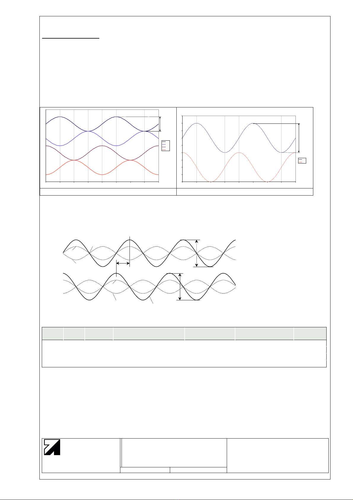
≥tpp
A
B
OREF
tpp: Minimum interval time
edge distance
/A
/B
Fig. 6 Output signals
For generating a reference pulse at the output and the exact assignment of the signals A, B and OREF it is
necessary to pass a Sin/Cos-period (for finding the zero degree angle). That status will be signalized by a
green Valid-LED (LED 3, looked status). In the case of an error the red Error-LED (LED 2) is switched on
and the green Valid-LED is switched off. An external reset pulse with a minimum length of 3µs will restart
the GC-IP1000. To get the locked status again a further Sin/Cos-period is needed.
In case of selected interpolation rates 125 and 250-fold the assignment of A, B and OREF can not be
guaranteed.
4.2 Error Signal
An error signal will be generated if the input signals are plausible no longer. The error signal will also be
generated if the input frequency is so high that the square-wave signals are unable to follow, and/or when
the maximum input frequency is exceeded.
If the error signal was activated, and/or if one of the error bits was set in the result register, the present
measuring result and all the following results would have to be discarded. Following elimination of the cause
of the error and a reset of the error bit, the reference point has to be passed by for absolute value
measurements once again!
5 Interpolation Rate
The interpolation rate can be set at 1000, 800, 500, 400, 250, 200, 125 and 100. The interpolation rate as
defined for the purposes of this application is the number of increments into which one sine period of the
input signal is divided. This also corresponds to the number of edge changes on the A/B output signals per
input signal period. This means that the number of square-wave periods at the Aand Boutputs totals 1/4 of
the interpolation rate per input signal period.
In the case that a standard interpolation counter or quadrature decoder is connected to the A/B outputs, this
has to work in "quadruple evaluation" mode in order to achieve the full interpolation rate.