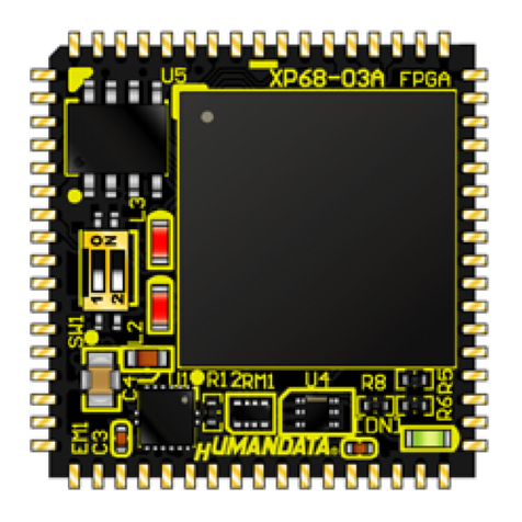
Humandata ACM-018 Series User manual

HuMANDATA LTD.
Cyclone III FPGA Board
ACM-018 Series (Rev2)
User’s Manual
Ver. 1.2

Table of Contents
Revision History.............................................................................................. 1
Introduction .................................................................................................... 1
1. Unused Pins [IMPORTANT] .............................................................................. 2
2. Specifications ..................................................................................................... 3
3. Overview ............................................................................................................ 4
3.1. Name of Parts.......................................................................................................4
3.2. Block Diagram......................................................................................................5
3.3. Power Supply........................................................................................................5
3.4. JTAG Connector ...................................................................................................6
4. Jumper Switches................................................................................................ 7
5. FPGA Configuration........................................................................................... 8
6. Configuration Device Programming ................................................................... 8
7. Additional Documentation and User Support ..................................................... 9

Precautions
Do Not
1. This product uses ordinary off-the-shelf electronic components, and is therefore inappropriate for use in
applications that require special quality or reliability and are expected to protect human lives or prevent
accidents, such as safety mechanisms in fields including space, aeronautics, medicine, and nuclear
power.
2. Do not be used underwater or in high-humidity environments.
3. Do not be used in the presence of corrosive gases, combustible gases, or other flammable gases.
4. Do not turn on power when circuit board surface is in contact with other metal.
5. Do not apply voltage higher than rated voltage.
Attention
6. This manual may be revised in the future without notice owing to improvements.
7. All efforts have been made to produce the best manual possible, but if users notice an error or other
problem, we ask that they notify us.
8. Item 7 notwithstanding, HuMANDATA cannot be held liable for the consequences arising from use of
this product.
9. HuMANDATA cannot be held liable for consequences arising from using this product in a way different
from the uses described herein, or from uses not shown herein.
10. This manual, circuit diagrams, sample circuits, and other content may not be copied, reproduced, or
distributed without permission.
11. If the product emits smoke, catches fire, or becomes unusually hot, cut the power immediately.
12. Be careful of static electricity.
13. This product may be subject to the export restrictions of Japan, the United States, or other countries.
Purchasers are responsible for properly observing export restrictions.
14. HuMANDATA firmly refuses to export (including reexporting) products to countries or regions subject to
export restrictions.
Product Warranty and Scope of Support
1. HuMANDATA guarantees that its products can be assembled as shown in published circuit diagrams and other design documents.
There may be differences between actual components or their prescribed quantities and model numbers and those shown in circuit
diagrams.
2. Except for the guarantee in item 1, above, no guarantees whatsoever are made. When assembling the product as shown in a circuit
diagram is impossible, and the problem can be solved by revising the diagram, HuMANDATA will revise the diagram. When a
problem can be solved only by replacing components or modifying the product, HuMANDATA will take back the product to replace it
with a properly functioning product.
3. If the problem is minor, HuMANDATA will sometimes describe how to make the revision or modification, and ask the customer to
solve the problem.
4. HuMANDATA will determine how to honor the warranty, as through repair, replacement, return, or other action. The customer cannot
specify what action to take.
5. FPGAs and other components used in products sometimes have characteristic defects. Returns and replacements are not possible
even if such defects are discovered, whether before or after purchase.
6. HuMANDATA shall not be obligated to inform customers about defects in the main components used in products.
7. HuMANDATA shall not be obligated to provide support for products, or to provide support for the software of other companies
needed to use HuMANDATA products.
8. Published documentation shall be limited to that published by HuMANDATA at the time of product purchase, and HuMANDATA shall
not be obligated to provide any other documentation.
9. When repairs or replacements are provided under warranty in Japan, purchaser shall pay shipping charges for shipping to
HuMANDATA, and HuMANDATA shall pay shipping charges for shipping to purchaser.
10. When shipping from outside of Japan, purchaser shall pay all expenses including shipping charges and taxes.
11. Under whatever circumstances, HuMANDATA shall provide support for its products for a maximum of one year after shipping from
factory.
12. The Warranty is not applicable and support ends in the event of fire, storm and flood damage, earthquakes, lightning strikes, and
other natural disasters, as well as conflict or other occurrences.
13. Purchaser is assumed to have read and understood all the above when purchasing a HuMANDATA product.
Limitation of Liability
1. Purchasers assume all liability associated with the use of this product.
2. HuMANDATA assumes no liability whatsoever for any direct, indirect, special, incidental, or consequential damages arising from the
use of this product, even if HuMANDATA has been advised of the possibility of such damage, whether legal or in tort.
3. At the time this product is purchased, items 1 and 2 above shall be deemed to have been confirmed by purchaser.
Trademarks and Other Considerations
1. This manual uses various companies’ trademarks in places.
2. HuMANDATA is this company’s registered trademark.
HuMANDATA’s Philosophy
1. HuMANDATA endeavors to raise product quality. We continually make detailed improvements and adjustments that are not shown
in circuit diagrams.
2. HuMANDATA actively publishes, on the Web and in other ways, information considered useful to customers. Examples would be
how to use FPGAs and how to use development tools.
3. HuMANDATA makes efforts for the long-term provision of products and for continuing their long-term support.
4. Instead of concealing small product problems and documentation errors, HuMANDATA makes them public.
5. HuMANDATA abides by Japanese law and its spirit. We make no transactions with purchasers who commit illegal acts.
1
ACM-018 Series v1.2
Revision History
Date
Revision
Description
Jul. 15, 2009
v1.0
Initial release
Oct. 2, 2009 v1.1 Upgrade a board version from C to D (add resistor array
RM3, 4)
Update a block diagram in Section 3.2
Feb. 16, 2012
v1.2
Delete Download cable connection example figure
Introduction
Thank you for buying our product ACM-018.
This is an evaluation board equipped with an Altera Cyclone III, power, reset, and
clock circuit and configuration device.
It can provide you with very convenient and easy-to-use environment.

2
ACM-018 Series v1.2
1. Unused Pins [IMPORTANT]
Some unused I/O pins are connected to GND or VCCINT (1.2 V).
Smaller FPGAs use those pins as general-purpose I/Os, but larger FPGAs use those
pins as GND or VCC.
Therefore, they must be set as “As input tri-stated”.
If you forget to set the pins properly, large current will flow and damage FPGA and
peripheral circuit.
To set the unused I/O pins follow the steps below:
1. Open “Assignments” and click “Device…”
2. Click “Device & Pin Options…” button
3. Open “Unused Pins” tab
4. Set Reserve all unused pins as “As input tri-stated”

3
ACM-018 Series v1.2
2. Specifications
Model Name
ACM-018-16C8 ACM-018-40C8
FPGA
EP3C16Q240C8N
EP3C40Q240C8N
Configuration Device
EPCS16SI16N (ALTERA, 16Mbit)
User I/Os
100
On-Board Clock
30 [MHz] (External inputs are available)
User Switches
1
User LED
1
Status LEDs
2 (POWER, DONE)
Power-On Reset
200 [ms] typ. (Configuration Reset Signal)
JTAG Connector
DIL 10-pin socket, 2.54 [mm] pitch
Power Input
DC 3.3 [V]
(Internal power is generated by an on-board regulator.)
PCB
4 Layer FR-4 t1.6 [mm] Immersion gold
Dimensions
3.386" x 2.126" (86 x 54 [mm])
Weight
29 [g] typ.
User I/O Connectors
66-pin through-hole
dia. 0.9 [mm], 100[mil]/2.54 [mm] pitch
Accessories
DIL 10-pin header (Mounted)
2 DIL 80-pin headers (Cuttable)
RoHS Compliance
YES
* There may be cases when compatible parts are used.

4
ACM-018 Series v1.2
3. Overview
3.1. Name of Parts
Component Side
Solder Side
Power & POR
User Switch
Config. Switch
User I/Os (CNA)
FPGA
Config. Device
JTAG
Oscillator
30 MHz
User I/Os (CNB)
Serial I/F
User LED
DONE LED
Power LED

5
ACM-018 Series v1.2
3.2. Block Diagram
3.3. Power Supply
This board operates from single DC 3.3 V power supply.
The external power supply should be sufficient and stabilized.
Please apply power to CNA and CNB with thick print
pattern or cable. Please connect all ground pins.
Notes
Cyclone-III
EP3C16/40
Q240C8N
Power Circuit
2.5 V
1.2 V
Power LED
(3.3 V)
DONE LED
Config Device
EPCS16
(16 Mbit)
User I/Os CNB
VIO(B) INPUT
External CLK
User I/Os CNA
3.3 V INPUT
External CLK
nCONFIG
50
Power-On Reset
Typ. 200ms
Config. Switch
50
JTAG
JTAG
Buffer
.JIC
Oscillator
30 MHz
User LED
User Switch
External CLK
External CLK

6
ACM-018 Series v1.2
3.4. JTAG Connector
This connector is used to configure the FPGA and program the configuration device
in-system.
Pin assignment is as follows.
CN1
Net Label
Signal Name
JTAG Pin
Signal Name
Net Label
XTCK
TCK
1
2
GND
GND
XTDO TDO 3 4 VCC (3.3 V) V33A
XTMS
TMS
5
6
-
-
- - 7 8 - -
XTDI
TDI
9
10
GND
GND
You can use Altera download cable. (ByteBlaster [II/MV] or USB Blaster)
Please pay attention not to attach cables in reverse.
1
2
9
10
Notice

7
ACM-018 Series v1.2
4. Jumper Switches
SW1 is used to set FPGA’s MSEL0, MSEL1, MSEL2. “ON” means “Low (Ground)
Position No.
1
2
3
4
Net Label
PSW1
MSEL2
MSEL1
MSEL0
Factory Setting
OFF OFF OFF OFF
Function
User Switch
Configuration Mode
MSEL2
MSEL1
MSEL0
PS Mode
ON ON ON
AS Mode
ON
OFF
ON
JTAG
Any Any Any
AS mode (Configuration device access) : SW1 (2, 4 ON)
MSEL0 = ON
MSEL1 = OFF
MSEL2 = ON
JTAG mode : SW1 (Any setting)
MSEL0 = Any
MSEL1 = Any
MSEL2 = Any
For more details, please see FPGA data sheets.
Notes

8
ACM-018 Series v1.2
5. FPGA Configuration
To configure the FPGA via JTAG, please refer to the following steps.
1. Open [Tools] menu, then click [Programmer].
2. Select [JTAG] from [Mode] list.
3. Open [Processing] menu, then click [Auto Detect].
4. Double-click [none] and select the sof file you made.
5. Check [Program/Configure] and [Verify].
6. Open [Processing] menu, then click [Start].
If configuration is completed successfully, the DONE LED will light up.
Advice
Check if FPGA device name you set is same as that on the board.
Please check unused pins setting. (See section.1)
Quartus II help will give you more information.
6. Configuration Device Programming
To program the configuration device via JTAG , you need to prepare jic (JTAG
Indirect Configuration) file. You can generate jic file from sof file using Quartus II.
Please refer to the following steps.
Generating jic file
1. Open [File] menu, then click [Convert Programming Files].
2. Select [JTAG Indirect Configuration File] from [Programming file type] list.
3. Select the device name which on the board from [Configuration device] list.
4. Fill the [File name] as you like.
5. Click [Add Device], then select [Device family] and [Device name].
6. Click [Add File…], then select the sof file for input file.
7. Click [Generate].
Programming Configuration Device
8. Open [Tools] menu, then click [Programmer].
9. Select [JTAG] from [Mode] list.
10. Open [Processing] menu, then click [Auto Detect].
11. Select the jic file you made.
12. Check [Program/Configure] and [Verify]
13. Open [Processing] menu, then click [Start].

9
ACM-018 Series v1.2
After programming is completed successfully, turn off and on the power.
Configuration data in the configuration device will be automatically loaded into the
FPGA.
Advice
Check if the configuration device name, FPGA device family name and
device name you selected in step 3 and 5 are same as those on the board.
Quartus II help will give you more information.
7. Additional Documentation and User Support
The following documents and other supports are available at
http://www.hdl.co.jp/en/spc/ACM/acm-018/
Circuit Schematic
Pin List
Dimensional drawing
PCB drawing
Net List
… and more.

Cyclone III FPGA Board
ACM-018 Series
User’s Manual
Ver. 1.2 ............................................Feb. 16, 2012
HuMANDATA LTD.
Address: 1-2-10-2F, Nakahozumi, Ibaraki
Osaka, Japan
ZIP 567-0034
Tel: 81-72-620-2002 (Japanese)
Fax: 81-72-620-2003 (Japanese/English)
URL: http://www.hdl.co.jp/en/ (Global)
http://www.hdl.co.jp/ (Japan)
This manual suits for next models
2
Table of contents
Other Humandata Control Unit manuals
Popular Control Unit manuals by other brands

YOODA
YOODA SMART CONTROL UNIT manual

HYDAC International
HYDAC International FCU 2110-5 Operating and maintenance instructions

Fluke
Fluke DTX-MFM user manual

Coolmay
Coolmay MX2NC PLC user manual

Spectrum Controls
Spectrum Controls SLC 500 user manual

Hattersley
Hattersley C31 Installation and operating instructions