HYT TM-610 User manual


TM-
610 Service Manual
1
Contents
General ...............................................................................................................................2
Radio Overview..................................................................................................................3
Software Specifications.....................................................................................................7
Circuit Description...........................................................................................................10
Semiconductor Data........................................................................................................14
TM-610 Parts List 1 ..........................................................................................................19
Tuning Description ..........................................................................................................58
Terminal Function............................................................................................................71
Troubleshooting Flow Chart ...........................................................................................75
Disassembly and Assembly for Repair..........................................................................79
Exploded View..................................................................................................................82
TM-610 Parts List 2 ..........................................................................................................83
Packing.............................................................................................................................85
TM-610 VHF PCB View.....................................................................................................86
TM-610 UHF PCB View ....................................................................................................88
TM-610 Block Diagram ....................................................................................................93
TM-610 VHF Schematic Diagram....................................................................................94
TM-610 UHF Schematic Diagram..................................................................................103
Specifications.................................................................................................................109

TM-610 Service Manual
2
General
Manual Scope
This manual is intended for use by experienced technicians familiar with similar types of communication equipment. It
contains all service information required for the equipment and is current as of the publication date.
Safety and General Information
Safety Standards
zThis equipment should be serviced by qualified technicians only.
zDo not modify the radio for any reason.
zUse only HYT supplied or approved antenna.
zInstall the mobile antenna at least 82cm (32 inches) away from your body, in accordance with the requirements
of the antenna manufacturer/supplier.
zTransmit only when people inside and outside the vehicle are at least 82cm (32 inches) away from a properly installed,
externally mounted antenna.
zTurn off your radio prior to entering any area with a potentially explosive atmosphere.
zTo avoid electromagnetic interference and/or compatibility conflicts, turn off your radio in any facility where posted
notices instruct you to do so.
zTo avoid possible interference with blasting operations, turn off your radio when you are near electrical blasting caps,
in a blasting area, or in areas posted: “Turn off two-way radio.” Obey all signs and instructions.
zFor vehicles with an air bag, do not place a radio in the area over an air bag or in the air bag deployment area.
zDo not expose the radio to direct sunlight over a long time, nor place it close to heating source.
zDo not place the radio in excessively dusty, humid areas, or on unstable surfaces.
Operation Safety Guidelines
zFor vehicles equipped with electronic anti-skid braking systems, electronic ignition systems or electronic fuel injection
systems, interferences may occur during the radio transmission. If the foregoing electronic equipments are installed
on your vehicle, please contact your dealer for further assistance to make sure that the radio transmission will not
interfere with these equipments.
zFor radio installation in vehicles fueled by LP gas with LP gas container within interior of the vehicles, the following
precautions are recommended for personal safety.
①Any space containing radio equipment shall be isolated by a seal from the space in which the LP gas container
and its fittings are located.
②Remote (outside) fitting connections shall be used.
③Good ventilation is required for the container space.
Installation Safety Guidelines
zDo not mount the mobile radio overhead or on a sidewall unless you take special precautions.
zIf the mobile radio is not properly installed, road shock could bump the radio loose, and the falling radio could, in
some circumstances, cause serious injury to the driver or a passenger. In case of vehicle accidents, even when
properly installed, the radio could break loose and become a dangerous projectile.

TM-
610 Service Manual
3
Radio Overview
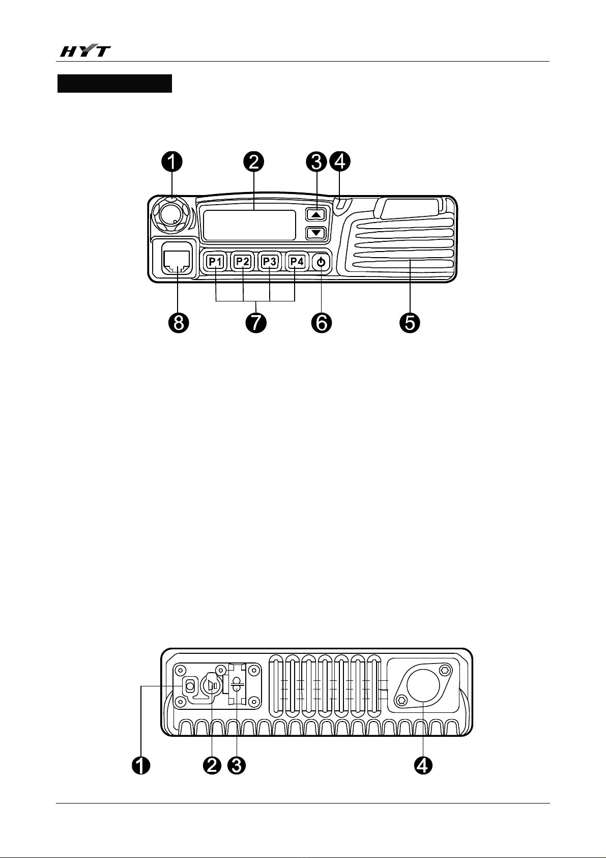
Front Panel View
①Volume Control Knob
Rotate the knob clockwise to increase the volume and counter-clockwise to decrease the volume.
②LCD
Please refer to section LCD Display.
③Programmable Function Keys ▲ / ▼
Your local dealer can program these keys with various auxiliary functions.
Please refer to section Programmable Function Keys.
④LED Indicator
⑤Speaker
⑥Power Switch
⑦Programmable Function Keys P1 / P2 / P3 / P4
Your local dealer can programmed these keys with various auxiliary functions.
Please refer to section Programmable Function Keys.
⑧Microphone Jack
Plug the microphone into the jack.
Rear Panel View

TM-
610 Service Manual
4
①15 Pin Connector (for external expansion)
②External Speaker Jack
Used to connect an external speaker with a 3.5 mm plug. Refer to Test Cable for Speaker Output in Tuning Description for
details.
③Power Inlet
Use HYT-authorized DC power cord to inlet 13.6 V DC power.
④Antenna Connector
Used to connect an external antenna.
Microphone
LED Indicator
Indicator Description
Light red Transmitting
Light green Receiving
Flash orange Receiving 5-Tone call
Light orange Transmitting call
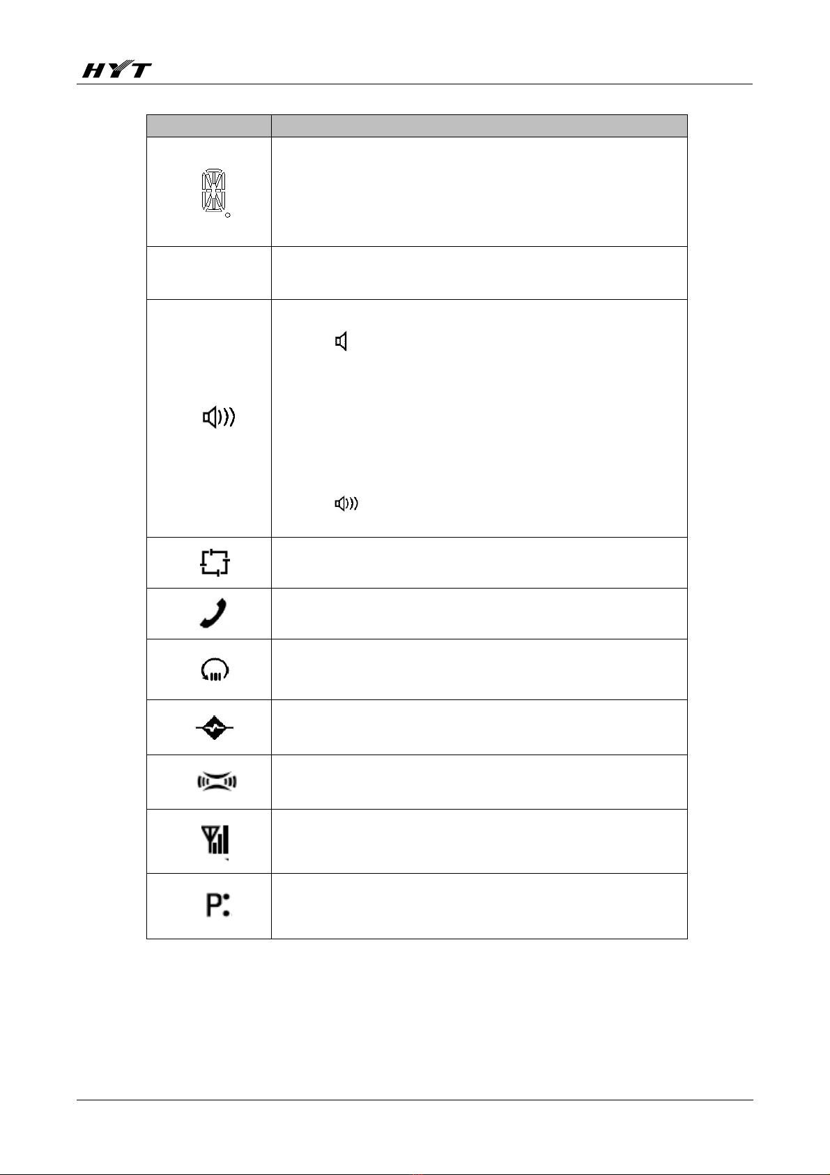
LCD Display
Figure 1 LCD Panel

TM-
610 Service Manual
5
Indicator Description
1. Display zone / channel number.
2. Display channel label
3. Display DTMF digit
4. Display channel Frequency
5. Display menu, setting items, etc.
Lo Display when the transmitting power is low.
The icon appears if any of the following conditions occurs:
1. Monitor status activated by pressing the Monitor key, and the channel
is initialized to Monitor Squelch.
2. Monitor status activated by a call or decoding, i.e., auto reset mode.
3. Monitor status activated by Force Monitor.
4. Carrier squelch mode under Rx Squelch.
5. Monitor status with authorization request.
The icon appears when speaker is unmated.
Appears when scan mode is active.
Appears during the auto reset time.
Appears when DTMF Keypad mode is enabled.
Appears when scrambler function is enabled.
Appears when compander function is enabled.
Appears when the selected channel is busy.
Appears when scan pauses on a priority channel. P•standards for
Priority Channel 1, P. standards for Priority Channel 2, and P: standards
for Priority Channels 1& 2.

TM-
610 Service Manual
6
Programmable Function Keys
[P1]-[P4], [▲ ]/ [▼ ] can be programmed with the following auxiliary functions:
1. None
2. CH Up
3. CH Down
4. Zone Up
5. Zone Down
6. Monitor/ Cancel Call
7. Cancel Call
8. Display Channel Alias
9. Display Freqency
10. Display Mode Switch
11. User Selectable Tone
12. Adjust Power Level
13. Scan
14. Nuisance Temporary Delete
15. Reverse
16. Talk Around
17. Adjust Squelch Level
18. Home Channel
19. Public Adress
20. Scrambler
21. Compander
22. AUX A
23. AUX B
24. Emergency
25. Call Forward
26. Wisper
27. Lone-Worker
28. Contact List
29. Status List
30. Channel Shortcut Button
31. Missed Calls
32. Received Calls
33. Keypad Mode
34. Menu
35. Call 1
36. Call 2
37. Call 3
38. Call 4
39. Call 5

TM-
610 Service Manual
7
Software Specifications
Radio Modes
1. Frame of Radio Modes
2. Keypad Entry for Mode Startup
Note: When power-on password is enabled, you must input the correct password before you can enter User Mode.
You can input password through the keypad and press [#] to clear.
MODE Main Menu Display/Sub Menu Operation Remarks
USER
MODE
Conventional
Mode ----------------------------
Turn on the radio to enter
Conventional Mode
ADJUST MODE ----------------------------
Press and hold [P1] to turn the
radio on.
Model Set Mode ----------------------------
Press and hold [P2] to turn the
radio on.
Firmware Version Display
Mode
---------------------------- While holding down [P4] key,
turn on the radio
Wired Clone Mode ----------------------------
While holding down [P3] key,
turn on the radio
PC Programming Mode ---------------------------- Receive commands from PC

TM-
610 Service Manual
8
3. Error Information and Measures in User Mode
The radio self-checks when power on. If no error is detected, the radio enters conventional mode. While the radio will
sound alert once any error is checked.
Error information and measures:
No. Error Information LCD Display Measures
1 Stun status Stun Re-program.
2 Data and Firmware Version mismatch No Data Re-program with programming software of right
version.
4. Firmware Version Display Mode
Turn the radio on while holding down [P4] to enter Firmware Version Display Mode, the firmware version will be displayed
on the LCD.
Release [P4] to enter User Mode.
5. PC Programming Mode
Connect the radio with a PC by programming cable. If data is written to the radio from PC, it can be programmed into the
EEPROM. Data programming is accessible by programming software.
When data is written to the radio from PC, “PROGRAM”appears on the LCD. LED glows green when data is written to the
radio and red when data is read from the radio. Radio will restart automatically when programming is completed.
6. Wired Clone Mode
Data can be transmitted from radio to radio by wired cloning.
(1) Turn on the source radio while holding down [P3] simultaneously, the radio enters Clone Mode with “CLONE”on
the LCD, or enters User Mode if Clone Mode is disabled by your dealer.
(2) Press [P3] to toggle between Dealer Clone and Factory Clone Mode. “DEACLONE”or “FACCLONE”appears on
the display when the corresponding mode is selected. The radio restores the original display after 5 seconds.
Unlike Factory Clone Mode, adjustment settings and embedded messages are not covered in Dealer Clone Mode.
Dealer Clone Mode is the default mode.
(3) Connect the two radios by cloning cable, then turn on the target radio.
(4) Press [P4] to start cloning, the LED of source radio glows red and that of target radio glows green during cloning.
“PROGRAM”is also displayed on the target radio. “END”appears on the source radio when cloning is completed
and the target radio enters user mode.
(5) Press [P4] to return to Clone Mode. “CLONE”appears on the source radio. Repeat the above steps to continue
wired cloning.
Note: Cloning is available only when both radios are in the same mode.
7. Panel Tuning Mode
The radio is tuned in this mode. Operations are as follows:
(1) Press [P1] to turn on the radio and enter tuning mode.

TM-
610 Service Manual
9
(2) Select the item with [Up]/[Down] keys. Press [P4] to enter the selected sub-item.
(3) Press [P4] to enter the sub-item and tune the data with [Up]/[Down] keys. Then press [P4] to save the data and
enter the next sub-item. Press [P1] to go back to the previous item without saving the data.
8. Model Set Mode
(1) Press [P2] to turn the radio on. The radio enters Model Set Mode. The frequency band appears on the LCD.
(2) Press [Up]/[Down] to choose right frequency band.
(3) Press [P4] to confirm. LED glows orange and ”WAIT”appears on the LCD; then the radio enters User Mode after
reset.
Notes:
1. Once [P4] key is pressed to set the new model, the previously stored channel data (frequency, CTCSS/CDCSS,
channel function settings) will be cleared, and part of functions also change. Therefore, do not make this operation unless
it’s necessary.
2. Initialization Data Table and frequency range (FL: lowest frequency- FH: highest frequency -FC: center frequency) of
different models are shown in the following table.
Model RX/TX 1 ( C ) 2 ( L ) 3 ( H ) 4 5 6 7 8
0 RX(MHz) 155.15 136.15 173.85 145.55 164.5 155 155.2 155.4
(V) TX(MHz) 155 136 174 145.5 164.5 155 155.2 155.4
1 RX(MHz) 435.15 400.15 469.85 417.55 452.5 435 435.2 435.4
(U1) TX(MHz) 435 400 470 417.5 452.5 435 435.2 435.4
2 RX(MHz) 475.15 450.15 499.85 462.55 487.5 475 475.2 475.4
(U2) TX(MHz) 475 450 500 462.5 487.5 475 475.2 475.4
3 RX(MHz) 495.15 470.15 519.85 482.55 507.5 495 495.2 495.4
(U3) TX(MHz) 495 470 520 482.5 507.5 495 495.2 495.4
4 RX(MHz) 375.15 350.15 399.85 362.55 387.5 375 375.2 375.4
(U4) TX(MHz) 375 350 400 362.5 387.5 375 375.2 375.4
5 RX(MHz) 455.15 440.15 469.85 447.55 462.55 455 455.2 455.4
(U5) TX(MHz) 455 440 470 447.5 462.5 455 455.2 455.4
6 RX(MHz) 503.15 480.15 525.85 491.55 514.55 503 503.2 503.4
(U6) TX(MHz) 503 480 526 491.5 514.5 503 503.2 503.4
7 RX(MHz) 340.15 330.15 349.85 335.05 345.05 340 340.2 340.4
(U7) TX(MHz) 340 330 350 335 345 340 340.2 340.4
TM600V: 136-174MHz
TM600U1: 400-470MHz
TM600U2: 450-500MHz
TM600U3: 470-520MHz
TM600U4: 350-400MHz
TM600U5: 440-470MHz
TM600U6 (for Taiwan only): 480-526MHz
TM600U7: 330-350MHz

TM-
610 Service Manual
10
CH 12345678
CTCSS Rx None None None CTS67.0HZ D023 CTS67.0HZ DI423 None
CDCSS Tx None None None CTS67.0HZ D023 CTS67.0HZ DI423 None
PWR Tx L L L L L L L L
CH CH 1 CH 2 CH 3 CH 4 CH 5 CH 6 CH 7 CH 8
NAME Wide Wide Wide Wide Wide Wide Wide Wide
Circuit Description
1. Frequency Configuration
The receiver utilizes double conversion superheterodyne. The first IF is 49.95MHz and the second is 450KHz. The first
local oscillator signal is supplied by the PLL circuit; and the second (50.4MHz) is generated from the frequency tripling of
TCXO (16.8MHz). The PLL circuit generates the frequencies required for transmission. (See figure 1).
Frequency Range VHF: 136MHz - 174MHz
UHF: 400MHz - 470MHz 450MHz - 500MHz
470MHz - 520MHz 350MHz - 400MHz
440MHz - 470MHz 480MHz - 526MHz
330MHz - 350MHz
2. Receiver Circuit
The receiver circuit is shown as figure 1.
Figure 1 Receiver Circuit
2.1 High Frequency Bandpass Amplifier Circuit
It consists of BPF, RF amplifier (Q111) and BPF (D110 and D111). The range of bandpass frequency is the frequency
range of the radio itself. The signal is filtered by the BPF to eliminate unwanted signals before going to the first mixer.
2.2 First Mixer
The signal from BPF is mixed with the first local oscillator signal from PLL circuit at the first mixer (D112) to become a
49.95MHz first IF signal. The first IF signal is then fed through the crystal filter (IF200) to further remove spurious signals.
2.3 IF Amplifier
The first IF signal is amplified by Q113 and then enters IC102 (TA31136FN), where the signal is mixed again with the

TM-
610 Service Manual
11
second local oscillator signal (50.4MHz) to become a 450KHz second IF signal. The second IF signal is then fed through a
ceramic filter (N: CF202; W: CF203) to eliminate unwanted signals. The resulting signal then is detected by IC102 and
output from Pin 9 as audio signals.
2.4 Audio Amplifier
The audio signal obtained from IC102 is amplified and filtered by IC402 before being amplified by IC401 (the received
signalling is separated and input into CPU for decoding). The processed signalling passes through Q406 (AF MUTE) and
is amplified by IC405. The amplified signal is fed to K301 controlling the volume and Q511 controlling SP MUTE on the
front panel before entering audio amplifier (IC511). The output audio signal drives the speaker.
2.5 Squelch Open
Part of the audio signals output from IC102 passes through IC102 Pin8 and is amplified by IC102 again, then is filtered
and rectified to produce an SQL level. The SQL level is compared with the existing reference level in CPU (IC502) to
generate a level to control AF MUTE and SP MUTE, which determines whether to output sounds from the speaker by
controlling Q406 and Q511.
3. Transmitter Circuit
The transmitter circuit is composed of the MIC circuit, modulation circuit, RF driver, final-stage power amplification circuit
and APC circuit.
Figure 2 Transmitter Circuit
3.1 MIC and Modulation Circuit
The audio signal from MIC is amplified by IC405 before being pre-emphasized and encoded by IC401. The output audio
signal is added into signalling and then is fed through VCO for modulation.
3.2 RF Driver and Final-Stage Power Amplification Circuit
The Tx-RF signal output from Q703 in the VCO circuit is amplified by Q101, drivers Q110 and Q109. The amplified signal
is then fed to IC101 (final-stage amplifier) and passes through LPF before reaching the antenna.
3.3 APC
The APC circuit stabilizes the output power at a predetermined level. D101 and D102 transform the signal from the
detector to DC voltage, which is then compared with the reference voltage from CPU in IC104 to output a DC voltage. The
DC voltage controls the output power by controlling the grid of IC101.

TM-
610 Service Manual
12
4. PLL Circuit
The frequencies of receiving the first local oscillator signal and transmitting signal are generated by the PLL circuit. The
PLL circuit consists of Tx frequency oscillator (Q701), Rx frequency oscillator (Q702), buffer amplifier (Q703), RF amplifier
(Q102), PLL IC (IC801), LPF and Tx/Rx VCO control switch (Q704, Q706).
In transmit mode, IC120 transmits the frequency data to PLL IC. Q704 is turned on to activate Tx VCO. The output signal
is amplified by Q703 and Q102, and then divided by PLL IC into 2.5KHz, 5KHz or 6.25KHz signals. The divided signal is
compared with the 2.5KHz, 5KHz or 6.25KHz reference signal from a 16.8MHz crystal oscillator (2.5 PPM frequency
stability) in the phase comparator. The frequency control voltage output from the phase comparator issent to Tx VCO after
passing through LPF (Q802, Q803). In the meantime, the modulation signal (Tx) is passed to Tx VCO for frequency
modulation.
The working principle in receive mode is similar to that in transmit mode.
Figure 3
5. Control Circuit
The control circuit is composed of CPU, reset IC and power supply control circuit.
5.1 CPU
IC502 (CPU) operates at 9.8304MHz. CPU controls the data transmission among E2PROM (IC501), Rx circuit, Tx circuit,
control circuit, display circuit and peripheral circuits.
Figure 4 Control Circuit

TM-
610 Service Manual
13
5.2 Power Supply
+B supplies power for the radio. D135 and D137 are over-voltage protection diodes. Power-on/off can be controlled via
the software.
Figure 5 Power Supply Circuit
Vout provides power for IC601, IC602 and IC803, which produces 8V, 5V, 3.3V voltage for the circuit.
6. Display Circuit
The display circuit is comprised of CPU (IC502), LCD, LED and other components. The radio can be manually operated
through P1 / P2 / P3 / P4 and ▲ / ▼ keys. Relevant channel information is displayed on the 15-segment LCD in
alphanumeric form.
Figure 6 Display Circuit

TM-
610 Service Manual
14
Semiconductor Data
1. Positive Voltage Regulator: TA7805F (POWER unit IC602) and TA7808S (POWER unit 601).
2. EEPROM: AT24C256N10SI2.7 (CPU unit IC501)
2.1 Pin Function
Pin No. Name I/O Function
1~3 A0~A2 I Address input
4 GND GND
5 SDA I/O Serial data
6 SCL Serial clock input
7 TEST Test
8 VCC +5V.
3. Audio Processor: AK2346 (AFPwr Unit IC404)
3.1 Pin Function
Pin No. Name I/O Function
1 AGNDIN I Analog ground input
2 AGND O Analog ground output
3 TxIN I Tx audio signal input
4 TxINO O TxA1 feedback output
5 LIMLV I Limit level tuning
6 EXTLIMIN I External signal input pin for pre-limiter circuit.
7 MOD O Modulated Tx signal output
8 VSS GND.
9 TCLK O Clock output pin for MSK transmission data.
10 TDATA I MSK transmission data input
Delay data is latched with the TCLK rising edge.
11 DI/O I/O Serial data input and output
Memory setting data during inputting; MSK receiving signal during outputting
12 RDF/FC O MSK signal output of receiving flag and frame detection signal
13 SCLK I I/O clock input of serial data
14 DIR I Serial data I/O control
15 XOUT I Crystal oscillator input
16 XIN I/O Crystal oscillator input and output
17 VDD Positive power supply
18 EXPOUT O Output signal after audio processing
19 RxAFIN I Rx audio signal input
20 RxAF O Rx audio signal output
21 RxLPFO O Rx LPF output
22 RxINO O RxA1 feedback output
23 RxIN I Demodulated Rx signal input
24 TEST I Test register control input
4. Audio Power Amplifier: TDA7297D (AFPwr unit IC511)
Pin Function

TM-
610 Service Manual
15
Pin No. Name I/O Function
1 PW GND Power ground 1
2 OUT1+ O Output 1+
3 N.C
4 N.C
5 OUT1- O Output 1-
6 VCC I Supply voltage
7 IN1 I Input 1
8 MUT I Operation switch
9 STAND-BY I Operation switch
10 PW GND Power ground 2
11 PW GND Power ground 3
12 N.C
13 SGND Signal ground
14 IN2 I Input 2
15 VCC I Supply voltage
16 OUT2- O Output 2-
17 N.C
18 N.C
19 OUT2+ O Output 2+
20 PW GND Power ground
5. LCD Driver: PCF8576DH (Display unit IC501)
Pin No. Name I/O Function
1 N.C.
2~7 S34~S39 O Output LCD.
8~9N.C.
10 SDA I/O Input/output I2C bus serial data
11 SCL O Output I2C bus clock
12 SYNC I N.C.
13 CLK I/O N.C.
14 VDD Power supply
15 OSC I Internal quartz crystal oscillator enable input
16~18 A0~A2 I Address line
19 SA0 I I2C bus sub-address bit 0
20 Vss GND
21 VLCD N.C
22~24 N.C.
25~28 BP0~BP3 O LCD base panel output
29~32 S0~S4 O Output LCD
33 N.C. .
34~47 S5~S18 O Output LCD
48 N.C.
49、50 S19、S20 O Output LCD
51~64 S21~S34 O Output LCD

TM-
610 Service Manual
16
6. Amplifier: TA75W558FU (AFPr unit IC404), TC75W51FU (AFPr unit IC402, AFPr unit IC405, AFPr unit IC403),
TA75S01F (RF unit IC1037), TA75W01FU (RF unit IC404).
7. IF Detector: TA31136FN (RF unit IC102).
8. Dual D-type trigger: TC4013BF (AFPwr unit IC512).
9. RF PLL Frequency Synthesizer: MB15A02 (PLL unit IC801).
10. CPU: SCM M3062LFGPGP (CPU unit IC502)
10.1 Pin Function
PIN No. Port Name Pin Name I/O Function
1 P94/DA1 APC O Modulated sensitivity output
2 P93/DA0 DTMF O DTMF/2-Tone/5-Tone/BEEP output
3 P92/ TB2in 2TN/5TN I 2-Tone/5-Tone decode pulse input
4 P91 AFDIO I/O AK2346 DATA I/O(SDAT)
5 P90 AFSCLK O AK2346 serial clock (SCLK)
6 BYTE BYTE I +5V(5C)
7 CNVSS CNVSS I GND (ground via 0 resistance)
8 P87 PA O MIC PA switch control,PA: H
9 P86 HMBL O Microphone backlight control
10 RESET RESET I Reset
11 XOUT XOUT O Clock output
12 VSS VSS I GND
13 XIN XIN I Clock input
14 VCC VCC I +5V
15 P85/NMI NMI I NMI (usually not used)
16 P84/INT2 AFRDF I Baseband chip MSK receive detect (RDF/FD)
17 P83/INT1 DTMFSTD I Not used (left open)
18 P82/INT0 AUX1 I/O Optional circuit board port 1(input)(renamed AUX1)
19 P81/TA4in SBC SB Power switch control,H: off,L: on
20 P80/TA4out CTC_OUT O CDCSS Balance
21 P77/TA3in SPMUTE O SP Mute,Mute: H
22 P76/TA3out CTC_PLL O CTCSS/CDCSS modulation output
23 P75/TA2in EMICC O External Mic control,External Mic: H (now NC)
24 P74/TA2out AFTDATA O Baseband chip MSK serial data (TDATA)
25 P73/TA1in AFTCLK I Baseband chip MSK serial clock (TCLK)
26 P72/TA1out AFDIR O Baseband chip I/O control pin (DIR)
27 P71/RxD2 RxD2 I Not used
28 P70/TxD2 TxD2 I Not used
29 P67/TxD1 TxD1 O Serial data output,PTT ON: L
30 P66/RxD1 RxD1 I Microphone HOOK input/serial data input,ON: L
31 P65 AUX4 I/O AUX4— — optional circuit board port 5 (output)
32 P64 AUX5 I/O AUX5— — optional circuit board port 6 (output)
33 P63 TxD2 O Acc comm0 (serial data output)
34 P62 RxD2 I Acc comm0 (serial data input)
35 P61 MICDAT I/O Microphone key code data input/output

TM-
610 Service Manual
17
36 P60 AUX2 I/O AUX2— — optional circuit board port 2 (input)
37 P57 RDY I Pull Up
38 P56 NC Not used (left open)
39 P55 HOLD Not used (left open)(for recording)
40 P54 NC Not used (left open)
41 P53 NC Not used (left open)
42 P52 RD O External expansion, read(Not used)
43 P51 NC Not used (left open)
44 P50 WR O External expansion, write(Not used)
45 P47 HNC O Horn alert control,ON: H,(Not used)
46 P46 SHIFT O Clock beat frequency,ON: H
47 P45 W/N O W/N switch,W: L,(change W to H)
48 P44 CS0 O NC (left open)
49 P43 MicMute O Mic mute,Mute: L,(change to H active)
50 P42 KEYBL O Keypad backlight control,ON: H, (NC)
51 P41 UP/LED4 O UP/LED4
52 P40 LED6 O LED6
53 P37 LCDCI/LED3 I/O LCD Driver CI PIN /LED3
54 P36 DOWN/LED5 O DOWN/LED5
55 P35 LCDCL/LED2 O LCD,Driver CL,PIN/LED2
56 P34 LCDBL/LED0 O LCD,Driver BL,PIN/LED0
57 P33 LED7 O LED7
58 P32 LCDCE/LED1 O LCD Driver CE PIN/LED1
59 P31 RLED O Red indicator
60 VCC VCC I +5V
61 P30 GLED O Green indicator
62 VSS VSS I GND
.63~66 A7~A4 A7~A4 I Not used (left open)
67 P23 PLLDAT O PLL data output
68 P22 PLLCLK O PLL clock output
69 P21 SLED O Scan status indicator
70 P20 PLED O High/low power indicator
71 P17 8RC O 8R power control,Rx: H
72 P16 8TC O 8T power control,Tx: H
73 P15 Rx O Tx/Rx VCO switch,Rx: L
74 P14 EEPDAT I/O EEPROM data input/output
75 P13 EEPCLK O EEPROM clock output
76 P12 PLLUL I PLL unlock detect,Unlock: L
77 P11 PLLSTB O PLL strobe output,Lock: L
78 P10 AFMUTE O Receive AF MUTE,Mute: H
79 P07 /IGN I Ignition sense input,H: off;L: on
80 P06 PWR I PWR key input,ON: L

TM-
610 Service Manual
18
81 P05 TYPE I TM-610/TM-610 Selection input,H: TM-610; L: TM-
610
82 P04 NC I Left open
83 P03 P4 I P4 input,ON: L (external pull-up resistor)
84 P02 P3 I P3 input,ON: L (external pull-up resistor)
85 P01 P2 I P2 input,ON: L (external pull-up resistor)
86 P00 P1 I P1 input,ON: L (external pull-up resistor)
87 AN7 Not used (left open)
88 AN6 Volume I Volume Tuning input
89 AN5 DTMF soft decode preserve
90 AN4 DTMF soft decode preserve
91 AN3 Temperature I Temperature data input
92 AN2 RSSI I RSSI input
93 AN1 SQL I SQL analog input
94 AVss AVss GND
95 AN0 TI I CTCSS/CDCSS signal input
96 VREF VREF I Reference voltage input
97 AVCC AVCC I +5V
98 P97/Sin4 AUX3 I/O Optional circuit board port 3 (INPUT)
99 P96/Sout4 AUX6 I/O Optional circuit board port 6 (OUTPUT)
100 P95/Clk4 APCO I/O Audio amplifer control port
Component Description
1. Tx-Rx Unit
Ref. No. Part Name Type Description
IC101 IC Power module Power module
IC501 IC AT2408N12.5S EROM
IC401 IC AK2346 Audio processor
IC404 IC TA75W558FU Dual operational amplifier
IC403 IC TC75W51FU Dual operational amplifier
IC803 IC XC62FP3302P Positive voltage regulator
IC602 IC TA7805F Positive voltage regulator
IC103 IC TA75S01F Single operational amplifier
IC104 IC TA75W01FU Dual operational amplifier
IC102 IC TA31136FN IF detector
IC502 IC M30624FCPGP#U5C CPU
IC121 IC BU4066BCFV Quad analog switch
IC122 IC LC73872M DTMF Rx circuit
IC125 IC M62364FP D/A converter with buffer amplifiers
IC126 IC TDA8561Q Power amplification
IC127 IC TC4013BF Dual D-type trigger
IC301 IC PCF8576DH LCD driver

TM-
610 Service Manual
19
TM-610 Parts List 1
Tx-Rx Unit (UHF)
No. Material No. Description Qty. Ref. No. Print No. Remarks
1 3001050000000 Chip resistor 0402 0ΩJ 1/16W 1 C404 B5E
2 3001050000000 Chip resistor 0402 0ΩJ 1/16W 1 R106 T2B
3 3001050000000 Chip resistor 0402 0ΩJ 1/16W 1 R110 T3B
4 3001050000000 Chip resistor 0402 0ΩJ 1/16W 1 R419 B5E
5 3001050000000 Chip resistor 0402 0ΩJ 1/16W 1 R448 B5F
6 3001050000000 Chip resistor 0402 0ΩJ 1/16W 1 R451 B5F
7 3001050000000 Chip resistor 0402 0ΩJ 1/16W 1 R455 T5F
8 3001050000000 Chip resistor 0402 0ΩJ 1/16W 1 R457 B5C
9 3001050000000 Chip resistor 0402 0ΩJ 1/16W 1 R480 T4B
10 3001050000000 Chip resistor 0402 0ΩJ 1/16W 1 R483 B4B
11 3001050000000 Chip resistor 0402 0ΩJ 1/16W 1 R485 T4F
12 3001050000000 Chip resistor 0402 0ΩJ 1/16W 1 R501 T4C
13 3001050000000 Chip resistor 0402 0ΩJ 1/16W 1 R509 T5F
14 3001050000000 Chip resistor 0402 0ΩJ 1/16W 1 R510 T4C
15 3001050000000 Chip resistor 0402 0ΩJ 1/16W 1 R513 T4C
16 3001050000000 Chip resistor 0402 0ΩJ 1/16W 1 R518 T5E
17 3001050000000 Chip resistor 0402 0ΩJ 1/16W 1 R520 T5E
18 3001050000000 Chip resistor 0402 0ΩJ 1/16W 1 R521 T5E
19 3001050000000 Chip resistor 0402 0ΩJ 1/16W 1 R522 T5E
20 3001050000000 Chip resistor 0402 0ΩJ 1/16W 1 R591 T5F
21 3001050000000 Chip resistor 0402 0ΩJ 1/16W 1 R600 T5F
22 3001050000000 Chip resistor 0402 0ΩJ 1/16W 1 R605 B2F
23 3001050000000 Chip resistor 0402 0ΩJ 1/16W 1 R608 T5F
24 3001050000000 Chip resistor 0402 0ΩJ 1/16W 1 R611 T4C
25 3001050000000 Chip resistor 0402 0ΩJ 1/16W 1 R620 T5F
26 3001050000000 Chip resistor 0402 0ΩJ 1/16W 1 R625 T5F
27 3001050000000 Chip resistor 0402 0ΩJ 1/16W 1 R627 T4C
28 3001050000000 Chip resistor 0402 0ΩJ 1/16W 1 R154 T4A U1:400-470MHz
29 3001053030010 Chip resistor 0402 30KΩJ 1/1 1 U2:450-500MHz
30 3001050000000 Chip resistor 0402 0ΩJ 1/16W 1 R153 T4A U1:400-470MHz
31 3001053320000 Chip resistor 0402 3.3KΩJ 1/ 1 U2:450-500MHz
32 3001051010000 Chip resistor 0402 100ΩJ 1/1 1 R146 T2D
33 3001051010000 Chip resistor 0402 100ΩJ 1/1 1 R197 T3A
34 3001051020010 Chip resistor 0402 1KΩJ 1/16 1 R145 B3A
35 3001051020010 Chip resistor 0402 1KΩJ 1/16 1 R200 T4A
36 3001051020010 Chip resistor 0402 1KΩJ 1/16 1 R439 B5E
37 3001051020010 Chip resistor 0402 1KΩJ 1/16 1 R453 B4F
38 3001051020010 Chip resistor 0402 1KΩJ 1/16 1 R476 B5B
39 3001051020010 Chip resistor 0402 1KΩJ 1/16 1 R503 T4C
40 3001051020010 Chip resistor 0402 1KΩJ 1/16 1 R504 T4C
Other manuals for TM-610
2
Table of contents
Other HYT Radio manuals