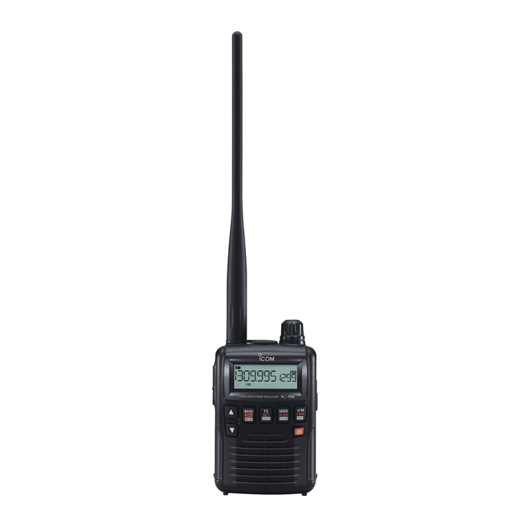
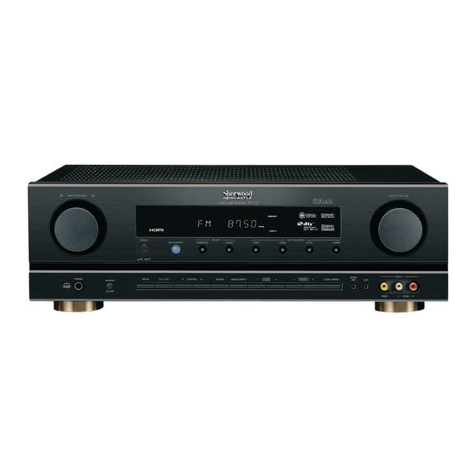
Icom IC-R5 User manual

SERVICE
MANUAL
COMMUNICATIONS RECEIVER
1-1-32, Kamiminami, Hirano-ku, Osaka, 547-0003, Japan S-13905IZ-C1
© 2002 Icom Inc.

INTRODUCTION
DANGER
ORDERING PARTS
REPAIR NOTES
This service manual describes the latest service information
for the IC-R5 COMMUNICATIONS RECEIVER at the time of
publication.
NEVER connect the receiver to an AC outlet or to a DC
power supply that uses more than 6.5 V. Such a connection
could cause a fire hazard and/or electric.
DO NOT expose the receiver to rain, snow or any liquids.
DO NOT reverse the polarities of the power supply when
connecting the receiver.
DO NOT apply an RF signal of more than 20 dBm (100mW)
to the antenna connector. This could damage the re-
ceiver's front end.
Be sure to include the following four points when ordering
replacement parts:
1. 10-digit order numbers
2. Component part number and name
3. Equipment model name and unit name
4. Quantity required
<SAMPLE ORDER>
8930058920 LCD contact IC-R5 LOGIC UNIT 5 pieces
8810009560 Screw PH BO M2x6 ZK IC-R5 CHASSIS 10 pieces
Addresses are provided on the inside back cover for your
convenience.
1. Make sure a problem is internal before disassembling the receiver.
2. DO NOT open the receiver until the receiver is disconnected from its power source.
3. DO NOT force any of the variable components. Turn them slowly and smoothly.
4. DO NOT short any circuits or electronic parts. An insulated turning tool MUST be used for all adjustments.
5. DO NOT keep power ON for a long time when the receiver is defective.
6. READ the instructions of test equipment thoroughly before connecting equipment to the receiver.
To upgrade quality, all electrical or mechanical parts and
internal circuits are subject to change without notice or oblig-
ation.
MODEL
IC-R5
Version
Europe
U.K.
Italy
U.S.A.
France
Spain
Export-01
Export-02
Canada
SYMBOL
EUR
UK
ITA
USA
FRA
ESP
EXP-01
EXP-02
CAN
AC ADAPTER
BC-149D
BC-149A
BC-149D
BC-149D
BC-136A
BC-136D
BC-149A

SECTION 1 SPECIFICATIONS
SECTION 2 INSIDE VIEWS
SECTION 3 DISASSEMBLY INSTRUCTIONS
SECTION 4 CIRCUIT DESCRIPITON
4-1 RECEIVER CIRCUITS . . . . . . . . . . . . . . . . . . . . . . . . . . . . . . . . . . . . . . . . . . . . . . . . . . . . .4-1
4-2 PLL CIRCUITS . . . . . . . . . . . . . . . . . . . . . . . . . . . . . . . . . . . . . . . . . . . . . . . . . . . . . . . . . . .4-3
4-3 OTHER CIRCUITS . . . . . . . . . . . . . . . . . . . . . . . . . . . . . . . . . . . . . . . . . . . . . . . . . . . . . . . .4-4
4-4 POWER SUPPLY CIRCUITS . . . . . . . . . . . . . . . . . . . . . . . . . . . . . . . . . . . . . . . . . . . . . . . .4-5
4-5 PORT ALLOCATIONS . . . . . . . . . . . . . . . . . . . . . . . . . . . . . . . . . . . . . . . . . . . . . . . . . . . . .4-6
SECTION 5 ADJUSTMENT PROCEDURES
5-1 PREPARATION . . . . . . . . . . . . . . . . . . . . . . . . . . . . . . . . . . . . . . . . . . . . . . . . . . . . . . . . . .5-1
5-2 PLL ADJUSTMENT . . . . . . . . . . . . . . . . . . . . . . . . . . . . . . . . . . . . . . . . . . . . . . . . . . . . . . .5-3
5-3 ADJUSTMENT MODE ADJUSTMENTS . . . . . . . . . . . . . . . . . . . . . . . . . . . . . . . . . . . . . . . .5-5
5-4 AUTOMATICALLY ADJUSTMENTS . . . . . . . . . . . . . . . . . . . . . . . . . . . . . . . . . . . . . . . . . . .5-8
SECTION 6 PARTS LIST
SECTION 7 MECHANICAL PARTS AND DISASSEMBLY
SECTION 8 SEMI-CONDUCTOR INFORMATION
SECTION 9 BOARD LAYOUTS
9-1 LOGIC UNIT . . . . . . . . . . . . . . . . . . . . . . . . . . . . . . . . . . . . . . . . . . . . . . . . . . . . . . . . . . . .9-1
9-2 RF UNIT . . . . . . . . . . . . . . . . . . . . . . . . . . . . . . . . . . . . . . . . . . . . . . . . . . . . . . . . . . . . . . .9-3
SECTION 10 BLOCK DIAGRAM
SECTION 11 VOLTAGE DIAGRAM
11-1 LOGIC UNIT . . . . . . . . . . . . . . . . . . . . . . . . . . . . . . . . . . . . . . . . . . . . . . . . . . . . . . . . . . . .11-1
11-2 RF UNIT . . . . . . . . . . . . . . . . . . . . . . . . . . . . . . . . . . . . . . . . . . . . . . . . . . . . . . . . . . . . . . .11-2
TABLE OF CONTENTS

1 - 1
SECTION 1 SPECIFICATIONS
MGENERAL
• Frequency range :
• Mode : FM, WFM, AM
• No. of memory channel : 1250 channel
(incl. scan edge and auto
memory right ch.)
• Frequency stability : ±6 ppm max.
(–10˚C to +60˚)
• Tuning steps : 5, 6.25, 10, 12.5, 15, 20,
25, 30, 50, and 100 kHz
• Anntena Impedance : 50 Ω
• Power supply requirement : 2 × AA(R6) Ni-Cd, alkaline
cells or external power
supply (BC-136, CP-17)
• Polarity : Negative ground
• Frequency resolution : 5 kHz, 6.25 kHz
• Current drain (at 3.0 V) :
Rated audio 170 mA typical
Standby 100 mA typical
Power saved 41 mA typical
(Power save ratio is 1 : 4)
• Usable temperature range : –10˚C to +60˚C
( –14˚F to +140˚F)
• Dimensions :
58(W) × 86(H) × 27(D) mm;
(projections not included)
29⁄32 (W) × 33⁄8(H) ×11⁄16(D) in
• Weight
(with antenna and battely)
: 185 (g); 6.5 (oz)
• External SP connector : 3-conductor 3.5(d) mm
(1⁄8”) / 8Ω
MRECEIVER
• Receiver system : Tripple super heterodyne
• Intermediate frequency : 1st 266.7 MHz
2nd 19.65 MHz
3rd 450 kHz
• Sensitivity* : (except spurious points)
* FM and WFM are measured at 12 dB SINAD; AM is measured
at 10 dB S/N.
• Squelch Sensitivity :
• Selectivity :
AM / FM more than 15 kHz / –6 dB
less than 30 kHz / –60 dB
WFM more than 150 kHz / –6 dB
• Audio output power : 100 mW typical at 10 %
distortion with an 8 Ωload
All stated specifications are subject to change without notice or obligation.
Version
EUR, U.K.,
ITA, ESP, CAN
EXP-01, EXP-02
U.S.A.
FRA
Receive Frequencies (MHz)
0.495 – 1309.995
0.150–823.995, 849.000–868.995,
894.000–1309.995
0.150–29.995, 50.200–51.200,
87.500–108.000, 144.000–146.000
430.000–440.000, 1240.000–1300.000
Frequency (MHz)
0.495 – 1.625
1.625 – 4.995
5.000 – 29.995
30.000 – 75.995
76.000 – 108.000
108.000 – 117.995
118.000 – 136.000
136.000 – 175.000
175.000 – 221.995
222.000 – 246.995
247.000 – 329.995
330.000 – 469.995
470.000 – 770.000
770.000 – 999.995
1000.000 – 1309.995
FM
—
0.32 µV
0.2 µV
0.18 µV
0.2 µV
0.18 µV
0.28 µV
0.35 µV
WFM
—
0.89 µV
—
0.71 µV
—
1.0 µV
—
AM
1.3 µV
0.71 µV
—
0.56 µV
—
0.56 µV
0.61 µV
—
Frequency (MHz)
0.495 – 1.625
1.625 – 5.0
5.0 – 30.0
30.0 – 76.0
76.0 – 108.0
108.0 – 118.0
118.0 – 136.0
136.0 – 175.0
175.0 – 222.0
222.0 – 247.0
247.0 – 330.0
330.0 – 470.0
470.0 – 770.0
770.0 – 833.0
833.0 – 1309.995
FM
—
0.56 µV
0.4 µV
0.56 µV
0.79 µV
WFM
—
5.6 µV
—
5.6 µV
—
5.6 µV
—
AM
2.5 µV
1.8 µV
—
1.8 µV
—
1.8 µV
—

SECTION 2 INSIDE VIEWS
•LOGIC UNIT
2 - 1
•RF UNIT
AF power amplifier
(IC450: TA31056F)
AF mute switch
(Q350: 2SJ144)
EEROM
(IC2: CAT24WC256)
AF filter
(Q301: XP6501)
+3.2 regurater
(IC103: R1111N321B)
DC-DC convertor
IC102: XC6371A351PR
D105: RB551V
Battery charger circuit
D503: MA133
D500: SB07-03C
Q501: 2SB-1132
()
()
Crystal bandpress filter
(Fl3: FL-293)
IF amplifer
(Q5: 2SC4215)
IF amplifier
(Q1 XP6501)
PLL circuit
AGC and AM detector
(Q4: XP6501)
Barantenra
tuning circnit
VCO circuit
Ceramic bandpass filter
(Fl1: EFCH266MKQP1)
BOTTOM VIEWTOP VIEW
1st mixer
(IC1: PC2757T)
PLL IC
(IC3: PD3140GS)
2nd mixer
(IC10: PC2757T)

SECTION 3 DISASSEMBLY INSTRUCTIONS
3 - 1
•REMOVING THE REAR PANEL
1Unscrew 2 screws, A.
2Remove the rear panel in the direction of the arrow.
•REMOVING THE RF UNIT
1Unscrew 1 screw, B.
2Unsolder 4 points, C.
3Remove 1 knob, and 1 cap G.
Unscrew 2 nuts, Eand F.
4Unplug, H, to separate the LOGIC unit, and then remove
the RF unit.
•REMOVING THE LOGIC UNIT
1Unsolder 2 points, I.
2Unscrew 2 screws, J, and then remove the LOGIC unit.
3Remove the LOGIC unit in the direction of the arrow.
A
Rear panel
J
LOGIC unit
I
B
C
D
H
RF unit
E
G
F
LOGIC unit

SECTION 4 CIRCUIT DESCRIPTION
4 - 1
4-1 RECEIVER CIRCUITS
4-1-1 BAND SWITCHING CIRCUIT (RF UNIT)
The RF signals from the antenna connector pass through the
limitter (D68) and an attenuator (D69). The signals are then
applied to the antenna switching circuit (D13, D31, D73, D75)
which suppress out-of-band signals.
4-1-2 RF CIRCUIT (RF UNIT)
The RF circuit amplifies the received signals within the range
of frequency coverage and filters out-of-band signals.
(1) 0.150 MHz–29.999 MHz
RF signals (0.150–29.999MHz) from an band switching cir-
cuit (D73) pass through a low-pass filter (C511–C515, L81,
L82). The filtered signals are amplified at an RF amplifier
(Q505) passing through each filters depending on the receiv-
ing frequency. The amplified signals are then applied to the
1st mixer circuit (IC1, pin 1) after being amplified at another
RF amplifier (IC11) via the band switching diode (D71).
The signals below 1.9 MHz pass through a low-pass filter
(C534, C535, C657, C658, L88, L89) via the band switching
diode (D66), and are then applied to the RF amplifier circuit
(Q505) via the band switching diode (D67).
The 1.9 MHz–14.995 MHz signals pass through the band
switching diode (D65) and bandpass filter (C522–C531,
L85–L87, L91), and are then applied to the RF amplifier cir-
cuit (Q505) via the band switching diode (D70).
The 15 MHz–29.995 MHz signals pass through the band
switching diode (D63) and high-pass filter (C516–C520, L83,
L84) and are then applied to the RF amplifier circuit (Q505)
via the band switching diode (D64).
(2) 118 MHz–174.995 MHz, 330 MHz–832.995 MHz
RF signals (118 MHz–174.995 MHz, 330 MHz–832.995
MHz) from an antenna switching diode (D75) are passed
through each bandpass filter and RF amplifier, and are then
applied to the 1st mixer circuit (IC1) via the band switching
diode (D71) and RF amplifier (IC11).
The 118 MHz–174.995 MHz signals pass through the band
switching diode (D74) and low-pass filter (C8–C13, C67,
C416, L14, L57–L59, L70), and are then amplified at RF
amplifier (Q14). The amplified signal passes through the tun-
able band-pass filters (D1, D2) and band switching diode
(D25).
The 330 MHz–469.995 MHz signals are amplified at RF
amplifier (Q35) via the band switching diode (D3) and band-
pass filter (C19–C23, C216, L2–L5). The amplified signal
passes through the tunable band-pass filters (D4, D5) and
band switching diode (D29).
The 470 MHz–832.995 MHz signals are amplified at RF
amplifier (Q24) via the band-pass filter (C32, C33, C35–C37,
C39, C145), between the band switching diode (D11, D32).
RF
RF
BPF
BPFBPF
RF BPF
RF BPF
RF BPF
RF
RF
BPF
BPF
Q26
Q36
Q35
Q24
Q14
D1, D2
D3, D11,
D74
D13, D31,
D73, D75
D63, D65,
D66 D64, D67,
D70
Q501, D76
Q505
0.15 30 MHz
118 175 MHz
330— 470 MHz
470 833 MHz
833 1309.995 MHz
30 118 MHz, 175 330 MHz
D4, D5
D32, D34
D36, D71 D25, D29,
D72
HPF
LPF
LPF
LIMITER
BAND
SW
BAND
SW
BAND
SW
BAND
SW
BAND
SW
BAND
SW BAND
SW
ANTENNA
ATT
ANT
SW
1st mixer
(IC1)
1st LO
IC11
2nd mixer
rcuit
• RF CIRCUIT

4 - 2
(3) 30–117.995 MHz, 175–329.995 MHz
The 30 MHz–117.95 MHz, 175 MHz–329.995 MHz signals
pass through the band switching circuit and low-pass filter
(C40–C43, C665, C666, L9, L10, L92), and are then applied
to the RF amplifier (Q36). The amplified signals are amplified
at the RF amplifier (IC11, pin 1) via band switching diodes
(D34, D71). The amplified signals are applied to the 1st mixer
circuit (IC1, pin 1).
(4) 833 MHz–1309.995 MHz
The 833 MHz–1309.995 MHz signals pass through the band
switching diode (D13) and bandpass filter (C5, C45–51,
L11–L13, L43), and are then applied to the RF amplifier
(Q26). The amplified signals are amplified at the RF amplifi-
er (IC11, pin 1) via band switching diodes (D36). The ampli-
fied signals are applied to 1st mixer circuit (IC1, pin 1).
4-1-3 1ST MIXER CIRCUIT (RF UNIT)
The 1st mixer circuit converts the received RF signals to a
fixed frequency of the 1st IF signal with a PLL output fre-
quency. By changing the PLL frequency, only the desired fre-
quency will pass through the bandpass filters at the next
stage of the 1st mixer.
The filtered RF signals are mixed with 1st LO signals at the
1st mixer circuit (IC1) to produce a 266.7 MHz 1st IF signal.
The 1st IF signal is output from pin 6, and passed through the
bandpass filter (FI1) to suppress unwanted harmonic com-
ponents. The filtered 1st IF signal is applied to the 2nd mixer
circuit.
The 1st LO signals are generated at the 1st VCO (Q28, Q30,
D54) and are applied to the 1st mixer (IC1, pin 3) directly or
passing through the doubler circuit (Q31) after being ampli-
fied at the buffer amplifiers (IC4, Q40).
4-1-4 1ST IF AND 2ND MIXER CIRCUITS (RF UNIT)
The 2nd mixer circuit converts the 1st IF signal to a 2nd IF
signal.
The filtered 266.7 MHz 1st IF signal from the bandpass filter
is mixed with the 2nd LO signal at the 2nd mixer circuit (IC10,
pin 1) to produce a 19.65 MHz 2nd IF signal. The 2nd IF sig-
nal pass through (except WFM mode) or bypass (WFM
mode) the bandpass filter (FI3), and is then amplified at the
2nd IF amplifier (Q5). The amplified signal is applied to the
demodulator circuit.
4-1-5 DEMODULATOR CIRCUITS (RF UNIT)
The demodulator circuit converts the 2nd IF signal into AF
signals.
The 19.65 MHz 2nd IF signal from the 2nd IF amplifier (Q5)
is applied to the 3rd mixer section of the FM IF IC (IC2, pin
16) and is then mixed with the 3rd LO signal for conversion
into a 450 kHz 3rd IF signal.
IC2 contains the 3rd mixer, limiter amplifier, quadrature
detector and S-meter detector, etc. A frequency from the PLL
reference oscillator is used for the 3rd LO signal (19.20
MHz).
(1) FM mode
The 3rd IF signal is output from the FM IF IC (IC2, pin 3) and
passes through the ceramic bandpass filter (FI2). The filtered
signal is fed back and amplified at the limiter amplifier section
(pin 5), then demodulated AF signals at the quadrature
detector section (pins 10, 11) and detector coil (L21). The
demodulated AF signals are output from pin 9 and are
applied to theAF circuit (LOGIC unit) via the “FMDET” signal.
16
Limiter
amp.
3rd IF filter
450 kHz
PLL IC
IC3
X1
19.2 MHz
RSSI
IC2 TA31136F
13 2nd IF (19.65 MHz)
from Q5
"RSSI" signal to the CPU
(LOGIC unit; IC1, pin 4)
11
10
9
87 53217 16
Active
filter
FI2
Noise
detector
FM
detector
LPF
Noise
comp.
"NOISE" signal to the CPU
(LOGIC unit; IC1, pin 47)
12
R54
R55
C101
C94
R56
C95
C98 C99
AM
DET. IF
amp.
C96
R57
R59 R60
WFM
L21
C93
C242
FM or WFM
AF signal "FMDET"
AM AF signal "AMDET"
Mixer
3rd
Q41
• DEMODULATOR CIRCUIT

4 - 3
(2) WFM mode
The 3rd IF signal from the 3rd mixer bypasses the ceramic fil-
ter (FI2) and fed back to the limiter amplifier section (pin 5).
The amplified signal is demodulated at the quadrature detec-
tor section (pins 10, 11) and detector coil (L21). The AF sig-
nals are output from pin 9 and are applied to the AF circuit
(LOGIC unit) via the “FMDET” signal.
By connecting R55 to R54 in parallel, the output characteris-
tics of pin 12, “RSSI”, change gradually. Therefore, the FM IF
IC can detect WFM components.
(3) AM mode
The filtered 3rd IF signal from the bandpass filter (FI2) is
amplified at the 3rd IF amplifier (Q1). The amplified IF signal
is applied to theAM detector circuit (Q4) to converted intoAF
signals, and the signals are applied to the AF circuit (LOGIC
unit) via the “AMDET” signal.
4-1-6 AF AMPLIFIER CIRCUIT (LOGIC UNIT)
TheAF amplifier circuit amplifies the demodulatedAF signals
to drive a speaker.
While in FM mode, AF signals from the demodulator circuit
(RF unit) are passed through the de-emphasis circuit (R323,
C316, C318) with frequency characteristics of –6 dB/octave,
and are then applied to the pre-amplifier (Q300) via the high-
pass filter (Q301).
While in AM mode, AF signals are pass through the high-
pass filter (Q301) and are then applied to the pre-amplifier
(Q300).
While in WFM mode,AF signals are applied to the pre-ampli-
fier (Q300) directly via the mode swtich (Q302).
The pre-amplified AF signals pass through the AF mute cir-
cuit (Q350) and are then applied to the electronic volume
control circuit (IC400, pin 6). The level controlled AF signals
are output from pin 7 and applied to the AF power amplifier
(Q452 and IC450, pin 1) via the buffer amplifier (Q400). The
power amplified AF signals are applied to the internal speak-
er via the [EXT SP] jack.
The electronic volume control circuit controls AF gain, there-
fore, theAF output level is according to the [VOL] setting and
also the squelch conditions.
4-1-7 SQUELCH CIRCUIT (LOGIC AND RF UNITS)
• NOISE SQUELCH
The noise squelch circuit cuts outAF signals when no RF sig-
nals are received. By detecting noise components in the AF
signals, the squelch circuit switches the AF mute switch.
A portion of the “NOISE” signals from the FM IF IC (RF unit;
IC2, pin 13) are applied to the CPU (LOGIC unit; IC1, pin 47).
The CPU analyzes the noise condition and outputs the
“AMUTE” signal (from pin 50) to the AF mute switch (LOGIC
unit; Q350).
• TONE SQUELCH
The tone squelch circuit detects AF signals and opens the
squelch only when receiving a signal containing a matching
subaudible tone (CTCSS). When tone squelch is in use, and
a signal with a mismatched or no subaudible tone is
received, the tone squelch circuit mutes the AF signals even
when noise squelch is open.
A portion of the AF signals from the FM IF IC (IC2, pin 9)
passes through the low-pass filter (LOGIC unit; IC200, pin 5)
via the “FMDET” line to remove AF (voice) signals and is
applied to the CTCSS decoder inside the CPU (LOGIC unit;
IC1, pin 7) via the “RTONE” line to control the AF mute
switch.
4-2 PLL CIRCUITS
4-2-1 PLL CIRCUIT (RF UNIT)
APLL circuit provides stable oscillation of the receive 1st/2nd
LO frequencies. The PLL circuit compares the phase of the
divided VCO frequency to the reference frequency. The PLL
output frequency is controlled by the divided ratio (N-data) of
a programmable divider.
Shift register
Prescaler
Phase
detector
Loop
filter
Programmable
counter
Programmable
divider
X1
19.2 MHz
to the FM IF IC
(IC2, pin 2)
"SHIFT" signal from CPU
(LOGIC unit; IC1, pin 62)
1st VCO
Buffer
Buffer
Buffer
Shift
switch Q40
Q43
IC4
3
4
5PSTB
IC3 (PLL IC)
PCK
PDAUL
to 1st mixer circuit
17
16
13 19
Q28, Q30, D54
Q2,
Q45
Q29, D46
• PLL CIRCUIT

4 - 4
An oscillated signal from the 1st VCO passes through the
buffer amplifiers (IC4, Q43) is applied to the PLL IC (IC3, pin
19) and is prescaled in the PLL IC based on the divided ratio
(N-data). The PLL IC detects the out-of-step phase using the
reference frequency and outputs it from pin 13. The output
signal is passed through the loop filter (Q2, Q45) and is then
applied to the 1ST VCO circuit as the lock voltage.
4-2-2 REFERENCE OSCILLATOR CIRCUIT
(RF UNIT)
The reference oscillator circuit (X1, D18) generates a 19.2
MHz reference frequency which is stabilized within the tem-
perature range –10˚C (+14˚F) to +60˚C (+140˚F). The refer-
ence frequency is applied to the PLL IC (IC3, pin 16) and the
signal is output from the pin 17, and is then applied to the FM
IF IC (IC2, pin 2) via the low-pass filter.
4-2-3 1ST VCO CIRCUIT (RF UNIT)
The oscillated signal is applied to the buffer amplifiers (IC4,
Q40). The amplified signal is applied to the 1st mixer circuit
(IC1) via the RX LO swtich circuit (D42–D44) and doubler cir-
cuit (Q31).
The 1st VCO circuit (Q28, Q30, D54) oscillates 266.85
MHz–380 MHz (normal) and 380 MHz–550 MHz (shifted) by
switching the SHIFT switch (Q29, D46) “High” and “Low”
respectively.
A portion of the signal from IC4 is amplified at the buffer
amplifier (Q43) and is then fed back to the PLL IC (IC3, pin
19) as the comparison signal.
4-2-4 DOUBLER CIRCUIT (RF UNIT)
The doubler circuit composes doubler1, doubler2 and bypass
circuits.
• DOUBLER1 CIRCUIT
The oscillated signal at the VCO circuit is amplified at the
buffer amplifier (IC4), and then applied to the other buffer
amplifier (Q40). The amplified 266.85–400 MHz signal pass-
es through the LO switch (D43), and is then applied to the
doubler circuit (Q31, pin 5). The signal is applied to the 1st
mixer circuit (IC1, pin 3) via the LO switch (D50).
• DOUBLER2 CIRCUIT
The oscillated signal at the VCO circuit is amplified at the
buffer amplifier (IC4), and then applied to the other buffer
amplifier (Q40). The amplified 380.45–549.85 MHz signal
passes through the LO switch (D44), and is then applied to
the doubler circuit (Q31, pin 6). The signal is applied to the
1st mixer circuit (IC1, pin 3) via the LO switch (D47).
• BYPASS CIRCUIT
The oscillated signal at the VCO circuit is amplified at the
buffer amplifier (IC4), and then applied to the other buffer
amplifier (Q40). The amplified 266.85–550 MHz signal
bypasses doubler circuit via the LO switch (D42, D52), and is
then applied to the 1st mixer circuit (IC1, pin 3).
4-2-5 2ND VCO CIRCUIT (RF UNIT)
The 2nd LO circuit generates the 2nd LO frequencies, and
the signals are applied to the 2nd mixer circuit.
The 2nd VCO circuit (Q6, D17, L45, C80, C207, C208) oscil-
lates 247.05 MHz and 286.35 MHz. The oscillated signal is
applied to the 2nd mixer (IC10, pin 3), and is then mixed with
the 1st IF signal.
An oscillated signal from the 2nd VCO passes through the
low-pass filter (C154, C250–C252, L69), and is applied to the
PLL IC (IC3, pin 2), and is then output from pin 8.
4-2-6 3RD LO CIRCUIT (RF UNIT)
The PLL IC (IC3) and X1 oscillate the 19.2 MHz LO signal.
The signal is applied to the PLL IC (pin 16), and is then
applied to the buffer amplifier section of the IC. The amplified
signal is output from pin 17, and is then applied to the 3rd
mixer section of the FM IF IC (IC2, pin 2) as 3rd LO signal.
4-3 OTHER CIRCUITS
4-3-1 BATTERY CHARGER CIRCUIT (LOGIC UNIT)
When the battery charger function is switched ON, the bat-
tery charger control signal becomes high, and is then output
from the CPU (IC1, pin 48) as “CHGC” signal. The signal is
applied to the battery charger controller (Q502), and its out-
put controls the battery charger circuit (Q501, D500, D503) to
output 120 mA charging current.
4-3-2 BAR ANTENNA TUNING CIRCUIT
(LOGIC AND RF UNITS)
When switching to theAM bar antenna whileAM band receiv-
ing, the AM bar antenna switching signal is output from the
CPU (LOGIC unit; IC1, pin 44) as “ANTSW” signal. The sig-
nal is applied to the antenna switching circuit (Q510, D76),
and then swtiches to the AM bar antenna.
The CPU (LOGIC unit; IC1) outputs the “TRAC” bar antenna
control signal from pin 141. The signal is applied to the level
convertor (RF unit Q513), and is then applied to the AM bar
antenna tune circuit (D100). The circuit tunes to the desire
frequency to change the D100’s capacity.

Q6, D17
VCO 2ND
VCO
Loop
filter
LPF
Q37, D53
+3S Ripple
filter
to the 2nd mixer (IC10, pin 3)
82
PLL IC
IC3
• 2ND VCO CIRCUIT

4 - 5
4-3-3 EAR PHONE ANTENNA CIRCUIT
(LOGIC AND RF UNITS)
When switching to the ear phone antenna while WFM band
receiving, the received RF signal passes through the exter-
nal speaker jack (LOGIC unit; J2). The signal is applied to the
D101’s anode side (RF unit), and is then applied to the RF
circuit.
4-3-4 RESET CIRCUIT (LOGIC UNIT)
When power switch is ON, +3CPU signal from the +3.2 reg-
ulator (IC103) is applied to the reset IC (IC3, pin 2). The IC
outputs reset signal via the “RESET” line, and the signal is
applied to the CPU (IC1, pin 19) to reset it.
4-3-5 LCD BACK LIGHT CIRCUIT (LOGIC UNIT)
When the LCD back lights ON, the LCD back light control sig-
nal becomes high, and is output from the CPU (IC1, pin 69)
as “LIGHT” signal. The signal is applied to the light swtich
(Q5), and is then applied to the LCD light LED (EP3).
LINE
HV
VCC
VP
+3CPU
+3V
+3S
R3V
DESCRIPTION
The voltage from the external power supply or
attached battery.
The same voltage as the “HV” line (external
power supply or battery pack).
Common 14 V converted from the clock signal
(LOGIC unit; IC1, pin 40) by the DC-DC conver-
tors (LOGIC unit; IC100, D100–D103). The out-
put voltage is applied to the PLL circuit, etc (RF
unit).
Common 3 V converted from the “VCC” line by
the +3.2 regulator IC (LOGIC unit; IC103). The
output voltage is supplied to the CPU, reset IC
(LOGIC unit; IC3), EEPROM (LOGIC unit; IC2),
etc.
Common 3 V converted by the +3 controller
(LOGIC unit; Q103) using the “PCON” signal
from the CPU. The output voltage is supplied to
the PLL IC (RF unit; IC3), etc.
Common 3 V converted by the +3S controller
(LOGIC unit; Q101, Q102) using the “PCON”
and “+3SC” signals from the CPU. The output
voltage is supplied to the ripple filter (RF unit,
Q37), etc.
Common 3 V converted by the R3V controller
(LOGIC unit; Q104) using the “+3SC” signal from
the CPU. The output voltage is supplied to the
buffer amplifier (LOGIC unit, Q400),AM detector
(RF unit; Q4), etc.
4-4 POWER SUPPLY CIRCUITS
VOLTAGE LINE

4 - 6
4-5 PORT ALLOCATIONS
4-5-1 CPU (LOGIC UNIT; IC1)
Pin Port Description
number name Pin Port Description
number name
2
3
4
5
6
7
14
15
19
25
26
28
30
31
32
33
34
43
44
45
46
47
K2
K1
RSSI
VIN
CTONE
RTONE
ESIO
ECK
RESET
POWER
HVDET
CLS
CLIN
CLOUT
PDAUL
PSTB
PCK
UHFC
ANTSW
WFM
AM
NOISE
Input port for the [∫], [√] switches.
Input port for the [BAND], [V/M],
[MODE] swtiches.
Input port for the RSSI signal from the
FM IF IC (RF unit; IC2, pin 12) to
detect receiving signal strength.
Input port for the power supply volt-
age.
• Input port for the antenna canceller
signal.
• Input port for the WX alert signal.
Input port for the CTCSS decode sig-
nal (67–254.1 Hz).
I/O port for the data signals from/to the
EEPROM (LOGIC unit; IC2, pin 5).
Outputs clock signal to the EEPROM
IC (LOGIC unit; IC2, pin 6).
Outputs reset signal to the CPU
(LOGIC unit; IC1, pin 19).
High:The CPU is reset.
Input port for the [POWER] switch.
Low: [POWER] switch is pushed.
Input port for the external power sup-
ply detecting signal.
Low: While external power supply is
connected.
Outputs clock shift control signal.
High:While clock is shifting.
Input port for the cloning data.
Outputs the cloning data.
Outputs data signal to the PLL IC.
Outputs strobe signals to the PLL IC
(RF unit; IC3, pin 3).
Outputs clock signal to the PLL IC (RF
unit; IC3, pin 4).
Outputs control signal for the UHF
band receiving.
Low: While receiving UHF band.
Outputs the AM bar antenna control
signal.
High:The AM bar ant. is selected.
Outputs control signal for the WFM
circuit.
Low: While receiving WFM mode.
Outputs control signal for the AM cir-
cuit.
Low: While receiving AM mode.
Input port for the SQL detection noise
signal.
48
49
50
51
52
53
54
55
58
59
60
61
62
63
64
65
66
67
68
Outputs the battery charger circuit
control signal.
High:While the battery is charging.
Outputs control signal for the CTCSS
regulator circuit.
Low: While CTCSS is ON.
Outputs control signal for the AF mute
circuit.
High:While muting.
Outputs control signal for the VHF
band receiving.
Low: While receiving VHF band.
Outputs the power swtich control sig-
nal.
Low: IC-R5 is power ON.
Outputs control signal for +3S and
R3V regulator circuits.
Low: Receiving.
Outputs control signal for the 15–30
MHz receiving.
Low: While receiving 15–30 MHz
band.
Outputs beep audio signals.
Outputs control signal for the 1.9–15
MHz receiving.
Low: While receiving 1.9–15 MHz
band.
Outputs control signal for the LO dou-
bler circuits.
Outputs the attenuator control signal.
Low: While attenuator is ON.
Outputs control signal for the VCO
shift circuit.
Outputs control signal for the 1.9–30
MHz receiving.
Low: While receiving 1.9–30 MHz
band.
Outputs control signal for the 0.5–1.9
MHz receiving.
Low: While receiving 0.5–1.9 MHz
band.
Outputs control signal for the 800 MHz
receiving.
Low: While receiving 800 MHz band.
Outputs control signal for the 300 MHz
receiving.
Low: While receiving 300 MHz band.
Outputs control signal for the 1200
MHz receiving.
Low: While receiving 1200 MHz
band.
Outputs control signal for the AF
amplifier regulator.
CHGC
TCON
AMUTE
VHFC
PCON
+3SC
B3C
BEEP
B2C
DBL2
DBL1
ATT
SHIFT
HFC
B1C
800MC
300MC
GC
AFON

4 - 7
Pin Port Description
number name
69
73
74
75
76
77
80–85
88–90,
92,
94–96
97
98
99–127
138
139
141
LIGHT
DCK
DUD
SQL
FUNC
MODE
RXF1,
RXF0,
B3–B0
SEC37–35,
SEG34,
SEC33–31
CONT1
CONT0
SEG28–0
VRC
FSET
TRAC
Outputs LCD back light control signal.
High:Lights ON.
Input port for the clock signal from the
[DIAL].
Input port for the up, down signals
from the [DIAL].
Input port for the [SQL] swtich.
Low: [SQL] swtich is pushed.
Input port for the [FUNC] swtich.
Low: [FUNC] switch is pushed.
Input port for the [MODE] switch.
Low: [MODE] switch is pushed.
Input port for the band matrix.
Outputs LCD segment data.
Outputs LCD contrast control signal.
Outputs LCD segment data.
Outputs audio volume level control
signal.
Outputs frequency control signal.
• Outputs vari-cap tuning control sig-
nal.
• Outputs bar antenna tuning control
signal.
CPU (Continued)

5 - 1
5-1 PREPARATION
Some adjustments must be adjusted on the adjustment mode. When entering the adjustment mode, the 68 kΩterminator is
required.
‘‘REQUIRED TEST EQUIPMENT
‘‘ENTERING THE ADJUSTMENT MODE
qConnect a 68 kΩterminator to the [SP] jack.
wPush and hold the [FUNC] key, and then turn power ON.
NOTE:
Entering adjustment mode, keep on entering adjustment mode until dis-connect the 68 kΩterminator and turn power
OFF.
■ OPERATION ON THE ADJUSTMENT MODE
Change the adjustment channel or item [UP] : [BAND] key
Change the adjustment channel or item [DOWN] : [TS] key
Change the adjustment value : [DIAL]
Verify the adjustment value : Push and hold [FUNC] key, and then push [BAND] key.
When entering adjustment mode, some adjustments need to push [V/M] or [FUNC] and [V/M] keys to write the adjustment
value to the CPU.
■ CONVENIENT!–AUTOMATICALLY ADJUSTMENT
BAR ANTENNA, VHF SENSITIVITY and UHF SENSITIVITY ADJUSTMENTS can be ajusted automatically.
The detail shows at page 5-8.
SECTION 5 ADJUSTMENT PROCEDURES
Pushing key
[V/M]
Operation
Start VHF and UHF SENSITIVITY ADJUSTMENTS automatically.
Set the REFERENCE FREQUENCY ADJUSTMENT value.
Set the S-METER ADJUSTMENT value.
Pushing key
Push and hold
the [FUNC] key,
and then push
the [V/M] key.
Operation
Set the VHF and UHF SENSITIVITY ADJUSTMENTS value when
manual adustment.
EQUIPMENT
DC power supply
DC voltmeter
Digital multimeter
GRADE AND RANGE
Output voltage : 3.0 V DC
Current capacity : 1 A or more
Input impedance : 50 kΩ/V DC or better
Input impedance : 10 kΩ/V DC or better
EQUIPMENT
Frequency counter
Standard signal
generator (SSG)
GRADE AND RANGE
Frequency range : 0.1–1000 MHz
Frequency accuracy: ±1 ppm or better
Sensitivity : 100 mV or better
Frequency range : 0.1–1300 MHz
Output level : 0.1 µV–32 mV
(–127 to –17 dBm)

5 - 2
to the antenna connector
Standard signal generator
0.1 V to 32 mV
( 127 dBm to 17 dBm)
Optional SMA BNC adaptor
1/8" (3.5 mm)
3-conductor plug
68 k
+
to [SP] jack
Power supply
6 V / 1 A
JIG
AD-92SMA
Power supply
3 V / 1 A
POWER SUPPLY CONNECTION
(IC-R5 has two pattern.)
Using [DC 6V] jack
CAUTION!
DO NOT input more than 3.0 V when
connect the power supply to the LOGIC
unit as shown right. Otherwise IC-R5 will
be damaged.
Connecting the power supply directly
• CONNECTION

5 - 3
5-2 PLL ADJUSTMENT
“REFERENCE FREQUENCY” adjustment must be performed at “ADJUSTMENT MODE”.
1ST VCO
LOCK
VOLTAGE
2ND VCO
LOCK
VOLTAGE
REFERENCE
FREQUENCY
DETECTOR
OUTPUT
VOLTAGE
ADJUSTMENT
ADJUSTMENT ADJUSTMENT CONDITION MEASUREMENT VALUE POINT
UNIT LOCATION UNIT ADJUST
1
2
3
4
5
1
2
1
1
• Displayed frequency :
493.300 MHz
• Receiving
• Displayed frequency :
493.300 MHz
• Receiving
• Displayed frequency :
282.900 MHz
• Receiving
• Displayed frequency :0.150 MHz
• Receiving
• Displayed frequency :
493.295 MHz
• Receiving
• Displayed frequency :
430.000 MHz
• Receiving
• Displayed frequency :
493.300 MHz
• Receiving
• Displayed frequency :
(Fr ch) 439.800 MHz
• Receiving
• Displayed frequency :
145.600 MHz
• Connect an SSG to the antenna
connector and set as:
Level : 1 mV*(–47 dBm)
Modulation : OFF
• Receiving
RF
RF
RF
RF
Connect the digital
multi-meter to the
check point LV1.
Connect the digital
multi-meter to the
check point V.
Connect the fre-
quency counter to
the check point F.
Connect the digital
multi-meter to check
point QUAD.
1.8 V – 2.8 V
1.8 V – 2.8 V
less than 12 V
1.4 V – 2.4 V
less than 12 V
0.4 V – 1.0 V
less than 2.6 V
706.4999 MHz –
706.5001 MHz
1.0 V
RF
LOGIC
RF
L63
Verify
Verify
Verify
Verify
Verify
[DIAL]
L21
*This output level of the standard signal generator (SSG) is indicated as SSG’s open circuit.

5 - 4
L21
DETECTOR OUTPUT VOLTAGE
adjustment
QUAD
DETECTOR OUTPUT VOLTAGE
check point
V
2ND VCO LOCK VOLTAGE
check point LV1
1ST VCO LOCK VOLTAGE
check point
F
REFERENCE FREQUENCY
check point
L63
1ST VCO LOCK VOLTAGE
adjustment
Bottom view
• RF UNIT

5 - 5
5-3 ADJUSTMENT MODE ADJUSTMENTS
• The following adjustments must be performed at “ADJUSTMENT MODE”.
• The following adjustments can be adjustned automatically. The detail shows “AUTOMATICALLY ADJUSTMENT”
(at page 5-8).
BAR
ANTENNA
VHF
SENSITIVITY
UHF
SENSITIVITY
ADJUSTMENT
ADJUSTMENT ADJUSTMENT CONDITION MEASUREMENT VALUE POINT
UNIT LOCATION UNIT ADJUST
1
2
3
4
1
2
3
4
1
2
3
4
• Displayed frequency :
(trL ch) 0.495 MHz
• Connect an SSG to the antenna
connector and set as:
Level : 40 mV*(–15 dBm)
Modulation : OFF
• Receiving
• Displayed frequency :
(trH ch) 1.620 MHz
• Set the SSG as
Level : 50 mV*(–13 dBm)
• Receiving
• Displayed frequency :
(trL ch) 118.100 MHz
• Connect an SSG to the antenna
connector and set as:
Level : 1 µV*(–107dBm)
Modulation : OFF
• Receiving
• Displayed frequency :
(trH ch) 174.900 MHz
• Receiving
• Displayed frequency :
(trL ch) 330.100 MHz
• Connect an SSG to the antenna
connector and set as:
Level : 1 µV*(–107dBm)
Modulation : OFF
• Receiving
• Displayed frequency :
(trH ch) 469.900 MHz
• Receiving
RF
RF
RF
RF
RF
RF
Connect DC volt-
meter to the check
point SEN.
Connect DC volt-
meter to the check
point SEN.
Connect the digital
multi-meter to the
check point SEN.
Connect DC volt-
meter to the check
point SEN.
Connect the digital
multi-meter to the
check point SEN.
Connect DC volt-
meter to the check
point SEN.
Maximum voltage
Maximum voltage
Maximum voltage
Maximum voltage
Maximum voltage
Maximum voltage
LOGIC
LOGIC
LOGIC
LOGIC
LOGIC
LOGIC
[DIAL]
[DIAL]
[DIAL]
[DIAL]
[DIAL]
[DIAL]
*This output level of the standard signal generator (SSG) is indicated as SSG’s open circuit.
• Push and hold the [FUNC] key, and then push the [V/M] key.

5 - 6
SEN
BAR ANTENNA check point
VHF SENSITIVITY check point
UHF SENSITIVITY check point
• RF UNIT
Bottom view

5 - 7
S-METER
ADJUSTMENT ADJUSTMENT CONDITION OPERATION
1
2
3
4
5
6
7
8
9
10
11
12
• Displayed frequency : (SM ch) 14.100 MHz
• Connect the SSG to the antenna connector and set as :
Level : 0.5 µV*(–113 dBm)
Modulation : OFF
• Mode : FM
• Receiving
• Set the SSG as :Level: 1.6 µV*(–103 dBm)
• Mode : WFM
• Receiving
• Displayed frequency : (SM ch) 145.100 MHz
• Set the SSG level : 0.5 µV*(–113 dBm)
• Mode : FM
• Receiving
• Set the SSG level : 1.6 µV*(–103 dBm)
• Mode : WFM
• Receiving
• Displayed frequency : (SM ch) 200.100 MHz
• Set the SSG level : 0.5 µV*(–113 dBm)
• Mode : FM
• Receiving
• Set the SSG level : 1.6 µV*(–103 dBm)
• Mode : WFM
• Receiving
• Displayed frequency : (SM ch) 435.100 MHz
• Set the SSG level : 0.5 µV*(–113 dBm)
• Mode : FM
• Receiving
• Set the SSG level : 1.6 µV*(–103 dBm)
• Mode : WFM
• Receiving
• Displayed frequency : (SM ch) 650.100 MHz
• Set the SSG Level : 0.5 µV*(–113 dBm)
• Receiving
• Set the SSG level : 1.6 µV*(–103 dBm)
• Mode : WFM
• Receiving
• Displayed frequency : (SM ch) 1100.100 MHz
• Set the SSG level : 1 µV*(–107 dBµ)
• Receiving
• Set the SSG level : 3.2 µV*(–97 dBm)
• Mode : WFM
• Receiving
*This output level of the standard signal generator (SSG) is indicated as SSG’s open circuit.
Push and hold the [MOD] key.
• Verify that S-Meter shows S4 (3dots).
ADJUSTMENT MODE ADJUSTMENTS (Continued)
• The following adjustments must be performed at “ADJUSTMENT MODE”.
Other manuals for IC-R5
3
Table of contents
Other Icom Receiver manuals

Icom
Icom IC-PCR1500 User manual

Icom
Icom IC-R1500 User manual

Icom
Icom IC-R5 User manual

Icom
Icom iC- r8500 User manual

Icom
Icom IC-R8600 Administrator Guide

Icom
Icom IC-R7100 User manual

Icom
Icom IC-R71 User manual

Icom
Icom COMMUNICATIONS RECEIVER IC-R3 User manual

Icom
Icom IC-R8600 User manual

Icom
Icom R-71A Installation guide

Icom
Icom IC-R72 User manual

Icom
Icom IC-PCR1000 User manual

Icom
Icom IC-R9500 User manual

Icom
Icom IC-R30 Manual

Icom
Icom IC-R5 Manual

Icom
Icom IC-R30 Setup guide

Icom
Icom IC-R9000L User manual

Icom
Icom IC-RP1510 User manual

Icom
Icom IC-R30 Installation guide

Icom
Icom IC-R9500 Installation and operating instructions