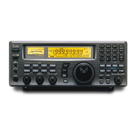
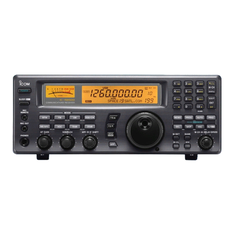
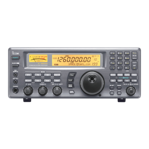
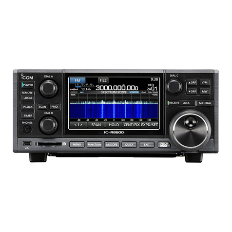
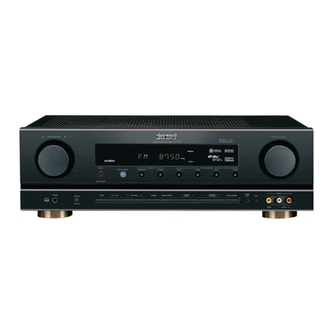
Icom iC- r8500 User manual

o
ICOM
SERVICE
MANUAL
Downloaded by
RadioAmateur.EU
COMMUNICATIONS RECEIVER
IC-R8500
loom Inc.

INTRODUCTION DANGER
This service manual describes the latest service information for
the IOR8500 COMMUNICATIONS RECEIVER at the time of
pubiication.
VERSION NO. VERSION SYMBOL
#02 U.S.A. USA
#03 Europe EUR
#05 France FRA
To upgrade quality, any electrical or mechanical parts and
internal circuits are subject to change without notice or
obligation.
NEVER connect the receiver to an AC outlet or to aDC power
supply that uses more than 16 V. This will ruin the receiver.
DO NOT expose the receiver to rain, snow or any liquids.
DO NOT reverse the polarities of the power supply when
connecting the receiver.
DO NOT apply an RF signal of more than 20 dBm (100 mW) to
the antenna connector. This could damage the receiver’s front
end.
ORDERING PARTS REPAIR NOTES
Be sure to include the following four points when ordering
replacement parts:
1.10-digit order numbers
2. Component part number and name
3. Equipment model name and unit name
4. Quantity required
cSAMPLE ORDER>
1130007700 S.iC BU4094BCF IC-R8500 PLL UNIT 5[>ieces
8810009030 Screw OHM3x8ZK IC-R8500 Topcover lOpieces
Addresses are provided on the inside back cover for your
convenience.
1.Make sure aproblem is internal before disassembling the
receiver.
2. DO NOT open the receiver until the receiver is
disconnected from its power source.
3. DO NOT force any of the variable components. Turn them
slowly and smoothly.
4. DO NOT short any circuits or electronic parts. An insulated
tuning tool MUST be used for all adjustments.
5. DO NOT keep power ON for along time when the receiver
is defective.
6. READ the instructions of test equipment thoroughly before
connecting equipment to the receiver.

TABLE OF CONTENTS
SECTION 1SPECIFICATIONS
SECTION 2INSIDE VIEWS
SECTION 3DISASSEMBLY AND OPTION INSTALLATIONS
3
-1DISASSEMBLY INSTRUCTIONS 3-1
3-2OPTION INSTALLATIONS 3-
1
SECTION 4CIRCUIT DESCRIPTION
4-1 RECEIVER CIRCUITS 4-1
4-2 PLL CIRCUITS 4-6
4-3POWER SUPPLY CIRCUITS 4-8
4-
4PORT ALLOCATIONS 4-8
SECTION 5ADJUSTMENT PROCEDURES
5-
1METER REFERENCE ADJUSTMENT 5-1
5-2POWER SUPPLY VOLTAGE AND PLL ADJUSTMENT 5-
1
5-3 RECEIVER ADJUSTMENT 5-3
5-4RF-B BPF TUNED VOLTAGE ADJUSTMENT 5-7
5-5NOISE SQUELCH. S-METER AND CENTER INDICATOR ADJUSTMENT 5-9
5-6 S-METER FLAT ADJUSTMENT 5-10
SECTION 6PARTS LIST
SECTION 7MECHANICAL PARTS
SECTION 8SEMI-CONDUCTOR INFORMATION
SECTION 9BOARD LAYOUTS
9-1 FRONT 9-1
9-2 MAIN UNIT 9-4
9-3 RF-AUNIT 9-6
9-4 RF-B UNIT 9-8
9-5VCO-A AND VCO-B BOARDS 9-9
9-6 PLL UNIT 9-10
9-7 MIX AND CONV UNITS 9-11
SECTION 10 BLOCK DIAGRAM
SECTION 11 VOLTAGE DIAGRAM

SECTION 1SPECIFICATIONS
•Frequency coverage:
Version Frequency coverage (MHz)
U.S.A
0.10000- 823.99889
849.00001- 868.99999
B94.0000I-1989.99999*
Europe
Australia 0.10000-1999.99999*
France 0.10000- 87.50000
108.00000-1999.99998*
^Specifications guaranteed 0. 1-1 000 and 1240-1 300 MHz.
•Mode ;SSB (USB. LSB)
CW (Normal, Narrow*)
AM (Wide. Normal. Narrow)
FM (Normal, Narrow)
WFM
•Number of memory:
•Antenna connector
:
•Usable temperature:
range
•Frequency stability
:
Tuning steps
•Power supply
requirement
•Current drain
(an 3.8 VDC)
•Dimensions
*Weight
*Optionai FU52A is required
1000 memory channels
plus 20 scan edge channels
and 1priority channel
below 30 MHz SO-239 (50 Q)
Phono: RCA (500 Q)
above 30 MHz Type-N (50 Q)
-10 1: to +50 1: :+14T to +1 22 *'f
below 30 MHz ±100 Hz (+20 Hz*)
above 30 MHz ±3ppm (+0.6 ppm*)
‘When the optional CR-203 is installed.
10, 50,100 Hz on, 2.5. 5. 9,10,
12.5, 20. 25. 100 kHz or 1MHz or
Programmable (0.5-1 99.5 kHz/
0.5 kHz step)
13.8 VDC ±15 %(negative ground)
or domestic AC with AD-55/A/V
Stand-by 1.8 A
Max. audio 2.0 A
287 (W) X112 (H) X309 (D) mm
11.3 (W)X 4.4 (H)x 12.2 (D) in
(projections not included)
7.0 kg: 15.4 lb
•Receive system :Superheterodyne system
Intermediate frequencies
Frequency band
(MHz)
1st
(MHz)
2nd
(MHz)
3rd
(kHz)
0.1- 29.99999 48.8 10.7 455*
30.0- 499.99999 778.7 10.7 455*
500.0-1024.99999 266.7 10.7 455*
Note: Convertor system is adopted above 1025 MHz.
Using local freq. of 500. 1000 or 1010 MHz.
•Except WFM
«Sensitivity
Frequency
band (MHz)
Mode
8SB/CW AM AM-N AM-W FM WFM
0.1-
0.49999 1.0 mV 6.3 mV --- -
0.5-
1.79909 2.0 mV 13.0 mV - - --
1.8-
1.09999 0.25 mV 3.2 mV 2.5 mV ---
2.0-
29.99999 0.2 mV 2.5 IW 2.0 mV -0.5 mV" -
30.0-
999.99999 0.32 mV 2.5 uV 2.0 mV 3.2 UV 0.5 mV 1.4 mV
1240.0-
1300.00000 0.32 mV 2.5 mV 2.0 mV 3.2 mV 0.5 mV 2.0 mV
Note: SSB, CW, and AM modes are measured at 10 dB S/N; FM
and WFM nrK>d6S are measured at 12 dB SINAD.
*0.5 uV is guaranteed in higher than 26 MHz for FM mode.
•Squelch sensitivity :
1.8-29.99999 MHz (threshold/tight)
SSB. CW, AM-N 10uV/320 mV
AM.AM-W 0.5uV/320mV
28-29.99999 MHz (thresholdAight)
FM 0.5 uV/320 mV
30-1000, 1240-1300 MHz (threshold/tight)
FM. AM, AM-W 0.4 uV/320 mV
WFM. SSB, CW, AM-N 4.5 uV/320 mV
•Selectivity
WFM More than 150 kHz/- 6dB
FM, AM-W More than 12 kHz/- 6dB
FM-N, AM More than 5.5 kHz/-6 dB
AM-N, SSB. CW. More than 2.2 kHz/- 6dB
CW-N (option) More than 0.5 kHz/-6dB
•Spurious and image rejection ratio
1.8-29.99999 MHz More than 60 dB
30-1000, 1240-1300 MHz 50 dB (typ.)
•Audio output power: More than 2.0 Wat 10%
(at 13.8 VDC) distortion with an 8Qload
•IF shift variable :More than ±1.2 kHz
range
•External speaker
connector
•RS-232C connector:
•Cl-V connector
•10.7 MHz IF out
connector
•AGC connector
•REC connector ;
•REC REMOTE :
2-conductor 3.5 (d) mm (Ve") /4-8 Q
D-subs 25
2-conductor 3.5 (d) mm (Va")
Phono: RCA (500)
Phono; RCA
2-conductor 3.5 (d) mm (Va")
connector
PHONES :3-conductor 6.35 (d) mm (V4")
connector
All stated specifications are subject to change without notice or obligation.
Downloaded by
RadioAmateur.EU
1-1

SECTION 2INSIDE VIEWS
•MAIN, RF-B AND MIX UNITS
AM demodulator
-
(015: 1SS375) •WFM demodulator
(IC2: MC3356DW)
AF power
(IC21: MPC1214H)
SSB, ON demodulator
(IC7: pPCl037GR)
FM demodulator
{IC8: MC3372SVM)
Bandpass inter (500-1025
Bandpass inter (242.
Bandpass inter (90-242. i
Bandpass lilier (30-90
RF-B unit
Mam CPU
(IC33: HD6433334YL01P)
mixer
(IC6: PPC1037GR}
unit
mixer
(ICitCBSOlMl)
>Bandpass inter
(R1: EZF-E778BT13)
-Notch filter
(FI2; E2F.E757AT11)
•PLL, CONV AND RF-A UNITS
CONV unit
RF converter
(IC2: 5MXF25-7)
RF amplifrer
MC1:GN1017. ^
IIC3: pPC2708tJ
PLL IC
(IC4; MC145190)
3rdLO DOS IC
(IC13: SC-1287)
8F0 DOS IC
(IC15: SC-1287)
Reference oscillator —
(Xl:CR-452 30-2 MHz)
DOS IC
(103: SC-1245)
RF-A unit
Antenna switch relay
(RL1: MZ-12HG)
—1st mixer
(Q6. Q7:2SK2171)
2nd mixer circuit
VCO-A board
IC
(ICIO; MC145190)
-PLL unit
Bandpass filler
(FI1:48M15A)
IC
(IC5: MC145190)
VCO-B board
2-1

3-1 DISASSEMBLY INSTRUCTIONS
.TOP AND BOTTOM COVERS
3-2 OPTION INSTALLATIONS
•FL-52A CW NARROW FILTER
®Remove the top cover as shown above.
(D Connect the FL-52A as shown in the diagram below.
•Make sure it is connected in the proper orientation.
Attached nuts on the FL-52A are not necessary. If you
want to install the filter more securely, open the MAIN
unit, then use the nuts on the bottom of the MAIN unit
d) Replace the top cover.
®Unscrew 6screws from the receiver's top and 4 screws
from the sides, then remove the top cover.
®Turn the receiver upside down.
d) Unscrew 6screws from the bottom cover, then remove the
bottom cover.
•UT-102 VOICE SYNTHESIZER UNIT
®Remove the top cover as shown above.
(D Remove the protected paper attached to the bottom of the
UT-102 to expose the adhesive strip,
d) Connect UT-1 02 as shown in the diagram below.
®Replace the top cover.

•CR-293 HIGH STABILITY CRYSTAL UNIT ©Remove the bottom cover as shown in the previous page.
@Unscrew 6screws as shown in the diagram, then remove
the shield plate and PLL cover.
®Unscrew 10screws from the PLL unit then open the unit to
expose the bottom.
®Unsolder the feet of the internal crystal unit, then remove it.
<f) Place the CR'293 in the space available as shown iq the
diagram, then solder its feet into place (6 points).
®Adjust the reference frequency using afrequency counter.
Ground
spring
nn63 0Replace the ground spring to its original position.
®Return the PLL cover, shield plate and bottom cover to
their original positions.
I
NOTE: The CR-293 is an oven-type crystal unit, and
the specified frequency stability described above is
guaranteed 1min. after power ON.
3'2

SECTION 4CIRCUIT DESCRIPTION
4-1 RECEIVER CIRCUITS
4-1-1 RF CONVERTOR CIRCUIT (CONV UNIT)
The RF convertor circuit converts 1025-1999.99999 MHz
RF signals to 200-989.99999 MHz RF signals.
(1) 30.00000-1024.99999 MHz signals
RF signals from the antenna connector (J1) pass through
the switching relays (RL1, RL2) to bypass the RF convertor
circuit. The bypassed RF signals either bypass or are
passed through the RF attenuator circuit (R17-R19.
R25-R27) then applied to the RF-B unit via J3.
(2) 1025.00000-1999.99999 MHz signals
RF signals from the antenna connector (J1) are applied to
the RF amplifier circuit (ICI, IC3) via the switching relay
(RL1) and tunable high-pass filter (D3-D5, D20, D21.
L2-L4). The amplified signals are mixed with convertor LO
signals at the RF convertor circuit (1C2) to produce
200.00000-989.99999 MHz RF signals. The converted RF
signals are applied to the RF-B unit via J3 after bypassing
or passing through the attenuator circuit.
The convertor PLL circuit (IC6; VCO, IC7: PLL 1C) gener-
ates a1000 or 1010 MHz LO signal and applies them to the
convertor circuit directly or divides them by 2at 108.
4-1-3 VHF/UHF RF CIRCUIT (RF-B UNIT)
The RF circuit amplifies the received signals within the
range of frequency coverage and fitters out-of-band signals.
The RF circuit consists of 4bandpass After circuits with an
RF amplifier for each.
The received signals from the CONV unit are passed
through to the tunable bandpass filter via the switching relay
(RL1), then ampliAed at the RF ampllAer circuit. The
amplified RF signals are again passed through another
bandpass Alter to suppress out-of-band signals. The Altered
signals are ampliAed at the other RF amplifier circuit (IC3),
then applied to the 1st mixer circuit after passing through
the low-pass or bandpass with tuned notch circuit.
The tunable bandpass Alters employ varactor diodes to tune
the center frequency of the RF passband for wide band-
width receiving and good image response rejection. These
diodes are controlled by the CPU (MAIN unit. IC33) via the
voltage amplifier circuit (IC2).
AGa-As FET is used for the RF ampliAers (Q1-Q4) to
provide high sensitivity within wide-band coverage, and also
to provide 10 dB amplifying gain.
•Convertor LO signals
Receive frequency Convertor LO frequency
1025-1199 99999 MKz 500 MHz
1200-1989 99999 MHZ 1000 MHz
1990-1999 99999 MHz 1010MHz
4-1-2 RF ATTENUATOR CIRCUIT
(CONV UNIT)
The attenuator circuit attenuates the signal strength up to
30 dB to protect the RF ampliAer from distortion when
excessively strong signals are received.
The RF attenuator circuit consists of 2separate attenuator
circuits connected in series. The 1st stage of the RF
attenuator circuit (R17-R19) provides 20 dB attenuation;
the 2nd stage (R25-R27) provides 10 dB attenuation via a
“n"type attenuator.
•Tunable bandpass filter and RF amplifier
Receive frequency
(MHz)
BPF select
signal Varactor diodes RF amp.
30.0- 89.99999 BPF1 D3. D4 Q1
90.0- 242.09999 BPF2 D9-D12 Q2
242.1- 499.99999 BPF3 D15, Die, D33, D34 Q3
500.0-1024.99999 BPF4 D19-D23 Q4
4-1-4 TUNED NOTCH CIRCUIT (RF-B UNIT)
The tuned notch circuit activates while RF signals higher
than 500 MHz are received. The circuit prevents the 1st LO
signal from entering the antenna connector and also re-
duces IF disturbance.
The tuned notch circuit {D29-D32, L51-L54, L74) is de-
signed between the high-pass (L82, C166-C168) and low-
pass Alter (L55, L56, C96-C98, Cl 00). The high-pass filter
reduces IF disturbance (266.7 MHz), and the tuned notch
and low-pass Alter circuits prevent the 1st LO signal from
entering the antenna connector.
•VHF/UHF RF and mixer circuits
30.0-1 999.9999a MHz CONV unit
30.0-989.99999 MHz
—
10 de
ATT
RF-B unit
^~^BPF2^
-^BPF3^
¥
BPF4/
Convertor LO signal
IC3
r^h
Bu^ -6<^
1st LO signal
2nd LO signal •
MIX unit
778.7 MHz
iC2
266.7 MHz
-<8>10.7 MHz
to
MAIN
unit
4-1
Varactor diodes are employed at the tuned notch filter
circuit to control the center frequency of the IF signal, and
are controlled by the CPU (MAIN unit, IC33) via the current
amplifier circuit (IC7a).
•Tuned notch filter characteristics
4-1-5 VHF/UHF 1ST MIXER CIRCUIT
(RF-B UNIT)
The 1st mixer circuit converts the received RF signals to a
fixed frequency of the 1st IF signal with aPLL output
frequency. By changing the PLL frequency, only the de-
sired frequency will pass through the bandpass filters at the
next stage of the 1st mixer.
4-1-6 VHF/UHF 1ST IFAND 2ND MIXER
CIRCUITS (MIX UNIT)
The 2nd mixer circuit converts the 1st IF signal to a2nd IF
signal.
The 1st IF signal from the RF-B unit is passed through the
bandpass filter to suppress unwanted out-of-band signals.
The 778.7 MHz 1st IF signal is passed through the dielectric
notch filter (FI2) to obtain good image response rejection for
the 21.4 MHz lower frequency from the receiving frequency
after passing through the dielectric filter (FH ).
And, the 266.7 MHz 1st IF signal is passed through the
helical notch filter (L15) to obtain agood image response
rejection for the 21 .4 MHz lower frequency from the receiv-
ing frequency via the helical bandpass filter (Li 4).
The filtered 1st IF signal is mixed with 2nd LO signals at the
2nd mixer circuit (ICI) to produce a10.7 MHz 2nd IF signal.
The 2nd IF signal is applied to the MAIN unit via J4 after
suppressing unwanted higher harmonic components at the
low-pass filter (L9, L22. C25, C27),
The 2nd LO signals are generated at the VCO-B circuit
(VCO-B board. Q1 ,Q3), and are applied to the 2nd mixer
circuit after being amplified at the LO amplifier circuit ()C2).
The filtered RF signals are mixed with 1st LO signals at the
1st mixer circuit (IC4, pin 3) to produce a778.7 or 266.7
MHz 1st IF signal. The 1st IF signal is output from pin 5,
and passed through the low-pass filter circuit (L75-L77,
Cl 41 -Cl 45) to suppress unwanted harmonic components.
The filtered 1st IF signal Is applied to the MIX unit via J2.
The 1st LO signals are generated at the VCO-A circuit
(VCO-A board, Q1, Q3), and are applied to the 1st mixer
(IC4, pin 6) after being amplified at the LO amplifier circuit
(IC6) via the VI LO line.
•1st LO frequency and 1st IF frequency
Receive freq. [MHz] 1st LO freq. [MHz] let IF freq.
(MHzj
30.0- 89.99999 808.7- 866.69999 778.7
90.0- 242.09999 868.7-1020.79999 778.7
242.1- 499.89999 1020.8-1278 69999 778.7
500.0-1024.99999 766.7-1291,69999 2B6.7
4-1-7 HF RF FILTER CIRCUIT (RF-A UNIT) '
The RF filter circuit consists of an antenna switching circuit,
9bandpass filters and an RF amplifier circuit.
IC-R8500 has 2antenna connectors for the HF bands
(ANTI and ANT2); ANTI employs an SO-239 connector
with 50 Qimpedance and ANT2 employs aphono/RCA
connector with 500 Qimpedance.
The RF signals from ANTI (J2) are applied to the bandpass
filter to suppress out-of-band signals via the antenna
switching relay (RLI). However, the RF signals from ANT2
(J1) are passed through the step-down transformer (LI) to
be converted into 50 Qimpedance when ANT2 is selected.
Then the RF signals are applied to the bandpass filter.
The filtered RF signals are bypassed or applied to the RF
amplifier circuit (Q1, Q2), depending on the syatus of the 10
dB attenuator, The RF amplifier circuit (Q1, Q2) provides
10 dB gain, therefore, the bypassed RF signal strength
seems attenuated when the 10 dB attenuator is turned ON.
•HF RF and mixer circuits
4-2

Then the RF signals from the switching diode (D17) are
applied to the 1st mixer circuit
•Bandpass filters
Receive freq.
{MHz]
SW
diode
BPF lelect
signal Components
0.1- 0.49999 D3 B1 L7.L8. C15-C17
0.5- 1.59999 D3 B2 LIO. L11.C22-C25
1.6- 1.99999 D7 B3 L23, L24, C42-C44
2.0- 3.99999 D8 B4 L18-L20. C34-C39
4.0- 7.99999 D8 B5 L26-L29, C46-C51
8.0-10.99999 D9 Be L31-U3. C54-C59
11.0-14.99999 D9 B7 L36-L38. C62-Ce7
15.0-21.99999 DIO B8 L41-L43, C70-C75
22.0-29.99999 DIO B9 L46-L49. C79-C84
4-1-8 HF 1ST MIXER CIRCUIT (RF-A UNIT)
The 1st mixer circuit converts the RF signals to adesired
48.8 MHz 1st IF signal. In this way, the VCO-A circuit
output frequencies are used for 1st LO signals after being
amplified at the LO amplifier (IC2).
The received RF signals from the bandpass filter circuit are
mixed with 1st LO signals at the 1st mixer circuit (06, Q7)
after passing through the low-pass filter circuit (LS9,
C98-C100). The mixed 1st IF signal is passed through the
crystal filter (FI1) to suppress out-of-band signals then
amplified at the IF amplifier circuit (Q8).
The amplified 1st IF signal is applied to the 2nd mixer
circuit.
•1st LO frequency and 1st IF frequency
4-1-10 IF CIRCUIT (MAIN UNIT)
The 10.7 MHz 2nd IF signal from the MIX unit Is applied to
the mode switch (D3) after being amplified at the IF ampli-
fier circuit (Q2). However, the 10.7 MHz 2nd IF signal from
the RF-A unit is applied to the mode switch (D3) directly.
The IF signal from the mode switch is then applied to a
different circuit depending on the receiving mode.
(1)
WFM mode
The 2nd IF signal from the mode switch (D3) is applied to
the IF amplifier circuit (Q4). The amplified IF signal is
passed through the bandpass fillers (Fll, FI2) to suppress
out-of-band signals. The filtered IF signal is then applied to
the WFM demodulator circuit.
(2) Other modes
The 2nd IF sign2Ufrom the mode switch (D3) is passed
through the bandpass filter (FI3) to suppress out-of-band
signals, and then applied to the IF amplifier circuit (Q15).
The amplified IF signal Is then applied to the 3rd mixer
circuit.
4-1-11 3RD MIXER CIRCUIT (MAIN UNIT)
The 3rd mixer circuit mixes the 2nd IF signal and 3rd LO
signal to produce a455 kHz 3rd IF signal. The 3rd LO
signal is generated at the DOS circuit (PLL unit, IC1 3) and
is applied to the 3rd mixer circuit via the buffer-amplifier
(Q28).
The 2nd IF signal from the IF amplifier circuit (Q15) is
applied to the 3rd mixer circuit (IC6, pin 6), and also the 3rd
LO signal (10.245 MHz) Is applied to pin 8of the 1C. The
mixed 3rd IF signal is output from pin 3, and is passed
through different bandpass fillers depending on the receiv-
ing mode and passband width. The filtered 3rd IF signal is
applied to the matched demodulator circuit with the receiv-
ing mode via the IF amplifier circuit (016).
Receive freq. [MHz] 1st LO freq. [MHz] 1st IF freq.
[MHz]
0.1-29.99999 48.9-78.79999 46.8
4-1-9 HF 2ND MIXER CIRCUIT (RF-A UNIT)
The 2nd mixer circuit converts the 1st IF signal to the
desired 10.7 MHz 2nd IF frequency. The 2nd LO signal is
used in the mixer circuit to produce a2nd IF frequency, and
the signal is generated at the VCO-B circuit (VCO-B board,
Q1 .Q3) after being amplified at the LO amplifier (IC1 ).
•Bandpass filter selection
Mode(s) Bandpass fitters) Passband width
FM. AM-W FI7. R6 12 kHz
FM-N, AM FIS. R6 5.5 kHz
SSB, CW. AM-N FI4 2.2 kHz
CW-N Optional FL-52A 500 Hz
4-1-12 DEMODULATOR CIRCUIT (MAIN UNIT)
The 1st IF signal from the IF amplifier (Q8) is applied to the
The demodulator circuit converts the 3rd IF signal into AF
signals. 4 separate demodulator circuits are employed for
4-3

(1)
WFM mode
The filtered 10.7 MHz 2nd IF signal from the bandpass filter
(FI2) is applied to the WFM demodulator circuit ()C2, pin 7).
The applied IF signal is mixed with an LO signal which Is
generated by XI to demodulate AF signals. The demodu-
lated AF signals are output from pin 13, and are then
applied to the squelch control gate (ICl9d).
(2) FM mode
The amplified 3rd IF signal at the IF amplifier (Q16) is again
amplified at the other IF amplifier (Q64) and then applied to
the FM detector circuit (ICS, pin 5). The applied 3rd IF
signal is mixed with the signal generated by discriminator
(X2) to demodulates AF signals. The demodulated AF
signals are output from pin 9and passed through the active
filter circuit (IC32a) to suppress unwanted subaudible tone
audio signals and lower noise components.
The filtered AF signals are applied to the squelch control
gate (ICl9c).
(3) AM mode
The amplified 3rd IF signal from the IF amplifier (Q16) is
again amplified at the other IF amplifiers (Ql7, Q18).
The amplified 3rd IF signal is then applied to the AM
demodulator circuit (015). The demodulated AF signals are
applied to the squelch control gate (IC19b).
(4) S5B and CW modes
The amplified 3rd IF signal from the IF amplifier (Q18) is
applied to the balanced mixer circuit (IC7) and mixed with
BFO signals to demodulate AF signals. The demodulated
AF signals are applied to the squelch control gate (ICl9a).
The BFO signals are generated at the BFO circuit (PLL unit,
IC15) and are applied to the balanced mixer circuit via the
buffer-amplifier (Q31).
4-1-13 SQUELCH CONTROL CIRCUIT
(MAIN UNIT)
The demodulated AF signals from the demodulator circuits
are applied to the squelch control gate (IC19). This con-
sists of 4analog switches which are selected with amode
signal 2und squelch control setting from the CPU (IC33) via
the expander 1C (IC18). The switched AF signals are
applied to the AF circuit.
4-
1-14 SQUELCH CIRCUIT (MAIN UNIT)
(1) FM. FM-N, AM and AM-W modes
Asquelch circuit cuts out AF signals when no RF signal is
received or the S-meter signal is lower than the [SQUELCH]
control setting level. By detecting noise components in the
AF signals, the CPU switches the squelch control gate.
Some noise components in the AF signals from pin 9of the
FM IF iC (ICS) are applied to the noise filter section in the
FM IF IC (pin 10). The filtered noise components are output
from pin 11, and then applied to the noise amplifier circuit
(IC9b). The amplified signals are rectified at the noise
detector circuit (D16) and the detected voltages are applied
to the CPU (IC33) via the NOAD line after being current-
amplified at the current-amplifier circuit (IC4a).
The [SQUELCH] control level signal is applied to the CPU
(IC33) via the sub-CPU (FRONT unit, IC1) as areference
voltage for comparison with the noise voltages. Also, an
5-
meter signal is applied to the CPU from the meter ampli-
fier (IC9a). The CPU compares these signals, then outputs
acontrol signal to the squelch control gate.
The FM IF IC detects noise components even in AM and
AM-W modes for noise squelch control, and also the IF
amplifier (Q18) is activated in FM and FM-N modes for
S-meter and S-meter squelch functions.
(2) WFM, S5B, CW and AM-N modes
The squelch circuit mutes AF output when the S-meJter
signal is lower than the [SQUELCH] control setting level.
*
SSB, CW and AM-N modes
Aportion of the 3rd IF signal from the IF amplifier (Q18) Is
converted into DC voltage at the AGC detector (Q27. D20)
and the meter amplifier (lC9a). The amplified signal is
applied to the CPU (IC33) via the SMAD line. The CPU
outputs control signals to the squelch control gate when the
S-meter signal is at alow level.
WFM mode
The WFM demodulator (IC2) controls input voltage of the
meter amplifier (IC9a, pin 2) via Q6 and the AGC line. The
same circuit is used even in WFM mode with SSB, CW and
AM-N modes.
•Squelch and AF amplifier circuits
4-4

4-1-15 AF AMPLIFIER CIRCUIT (MAIN UNIT)
The AF amplilier circuit amplifies the demodulated AF
signals to drive aspeaker.
AF signals from the squelch control gate are pre-amplified
at the AF amplifier (IC20) and are then applied to the AF
power amplifier (1C21) after either passing through or by-
passing the APF circuit (IC29-IC31, IC39). The power
amplified AF signals are applied to the Internal speaker via
the [EXT SP] and [PHONE] jacks when no plugs are con-
nected to the jacks.
The [AF GAIN] control signal is also applied to the AF
pre-amplifier (IC20. pin 8) via the CPU (IC33) to control
amplifying gain.
4-1-16 NOISE BLANKER CIRCUIT
(MAIN UNIT)
The noise blanker circuit detects pulse-type noises, and
stops IF amplifier operation during detection.
Aportion of the 3rd IF signal from the bandpass filter (FIS)
is amplified at the noise amplifier circuit (Q9, 105, Q11).
The amplified signal is rectified at the noise detector circuit
(DiO) for conversion into DC voltage. The DC voltage is
applied to the NB control circuit (Q12, Q13) to control the
NB switch (Q14).
Some DC voltage is fed back to the noise amplifier circuit
(ICS) via the DC amplifier (QIO). The DC amplifier function
as an AGC circuit to reduce averaged noise. Therefore, the
noise blanker function shuts off pulse-type noise only.
4-1-17 AGC CIRCUIT (MAIN UNIT)
The AGC (Auto Gain Control) circuit reduces IF amplifier
gain to keep the audio output at aconstant level.
Aportion of the 3rd IF signal from the IF amplifier (Q18) is
applied to the AGC detector circuit (D20). The detected
signal is applied to the AGC control circuit (Q20, Q21 ,Q25,
Q27) and then applied to the IF amplifiers (Q2, Q4,
Q15-Q17). The AGC voltage is also applied to the RF-A
and RF-B unit via the current-amplifier circuit (lC32b). The
current-amplified AGC signal is applied to the IF amplifier
and AGC control circuit in the RF-A unit (IF amp.: Q8, AGC
control: Q3), and the buffer-amplifier circuit in the RF-B unit
(ICIa).
When strong signals are received, the detected voltage
increases and the output level of the AGC control circuit
decreases. The AGC voltage is used as the bias voltage for
the IF amplifiers, therefore, the IF amplifier gain is de-
creased.
AGC response time is controlled by changing the time
constant at the AGC control line with resistors (R179, R180,
R503) and capacitors (C134-C137). R179. R180, Cl 34
and C135 are used for AGC slow, and R503, C136 and
Cl 37 are used tor AGC fast mode's time constant. The
time constant for AGC slow is connected to the AGC control
line- while AGC is set to slow. However, it's disconnected
from the AGC control line, and the time constant for AGC
fast is connected to the AGC control line while AGC is set to
fast. Both time constants are disconnected from the AGC
control line while scanning or when WFM or FM mode is
selected for faster response than AGC fast mode.
4-1-18 S-METER CIRCUIT (MAIN UNip
The S-meter circuit indicates the relative received signal
strength while receiving and changes depending on the
received signal strength.
Aportion of the AGC signal is applied to the meter amplifier
circuit (IC9a). The amplified signal is then applied to the
CPU (IC33) as an SMAD signal to drive the S-meter.
*
The SMAD signal is also used for noise and S-meter ^
squelch operation by comparison with the [SQUELCH]
control setting level and receiving signal strength at the
CPU.
4-1-19 APF CIRCUIT (MAIN UNIT)
The APF (Audio Peak Filter) circuit boosts aspecified
frequency to pick up desired CW signals, etc.
When [APF] is turned ON, the AF signals from the squelch
control gate (IC19) are applied to the APF circuit
(IC29-IC31, IC39). The [APF] control adjusts the peak
frequency within 200-1 000 Hz. IC29 is atriple 2-channel
analog switch IC and the AF signals are either passed
through or bypass the APF circuit.
The APF circuit functions as atone control while WFM, FM,
AM or SSB mode is selected.
•Noise blanker and AGC circuits
4-5

4-1-20 CENTER DETECTOR AND CENTER
INDICATOR CIRCUITS (MAIN UNIT)
(1)WFM and FM modes
Aportion of the detected audio signals from the demodu-
lator circuit (IC2 tor WFM, ICS for FM) are applied to the
center detector circuit (IC4b). The applied audio signals are
converted into DC voltage, and also amplified at the center
detector. The output DC voltage is then applied to the CPU
(IC33) as aCMAD signal for center indication and AFC
(Auto Frequency Control) operation, and is also applied to
the window-comparator (IC1 3) for center scan stop.
The output signal from the window-comparator is applied to
the CPU as aSTOP signal.
(2) AM mode
Aportion of the 3rd IF signal from the IF amplifier (Q18) is
amplified at the buffer-amplifier circuit (Q$5), and then
converted into an IF phase signal at the AM center circuit
(IC40c). The BFO signal is applied to the AM center circuit
(IC40d) to be converted into aBFO phase signal after being
amplified at the buffer-amplifier (Q66).
Both IF and BFO phase signals are applied to the phase
detector circuit (IC41) to detect phase differences. The
phase detector circuit outputs pulse-type signals according
to the phase difference from pin 8. and the output signals
are rectified at the rectifier section (060). The rectified
signal is then applied to the CPU (IC33) as aSTOP signal
via Q67 and Q68.
4-1-21 VSC CIRCUIT (MAIN UNIT)
The VSC (Voice Scanning Control) detects the AF signals
during scanning and skips undesired signals such as unmo-
dulated, beat and noise component signals.
Aportion of the AF signals from the squelch gate (IC19) are
applied to the VSC control circuit (IC10-IC12, Q30) after
being amplified at Q62. The amplified AF signals are
amplified and limited at the two-step amplifier section (ICl 0)
then the output signal is applied to the one-shot multi circuit
(IC11) as atrigger signal. The one-shot multi circuit func-
tions as an F-V convertor, and the output voltage is propor-
tional to the number of pulses within the singular time.
The output signals from the one-shot multi circuit are
passed through the low-pass filter (ICl 2a) to detect AF
signals. The filtered signals are then applied to the window
comparator (ICl2b). The window comparator outputs a
high level signal when the applied signals from the low-pass
filter exceeds the reference voltage.
The output signal is applied to the CPU (IC33) as aVSC
signal via IC1lc.
4-2 PLL CIRCUITS
4-2-1 1ST LO PLL CIRCUIT (PLL UNIT)
The 1st LO circuit generates the 1st LO frequency, and the
signals are applied to the 1st mixer circuit in the RF-A and
RF-B units. The 1st LO circuit consists of aDOS, VCO-A
circuits and PLL 1C, etc.
(1) DDS loop circuit
The signal generated at the VCO circuit (Q2, D1, D2) is
amplified at the buffer-amplifier (03) then applied to the
DDS circuit (ICS). The DDS circuit generates digital signal
using the applied signal as aclock frequency. The phase
detector section in IC3 compares it’s phase with the refer-
ence frequency which is generated at the reference oscil-
lator (XI ;30.2 MHz). 1C3 outputs off-phase components as
pulse signals via pins 52, 53.
The output pulses are converted into DC voltage at the loop
filter circuit (Q44, Q45) and then applied to the VCO circuit
to generate an approx. 6.5 MHz reference signal for the
main loop circuit.
The D/A convertor (R10-R33), bandpass filler (FM) and
buffer-amplifier (IC4) circuits are connected to the DDS
output to convert the digital oscillated signals into smooth
analog signals.
(2) Main loop circuit
The generated signal from the VCO-A circuit (VCO-A board,
Q1, 03) is buffer-amplified at the buffer-amplifier (ICS). The
buffer-amplified signal is applied to the prescaler section in
the PLL 1C (ICS. pin 11) via the low-pass filter circuit (L74.
L75, C263-C267). The applied signal from the VCO-A
circuit is prescaled In the PLL 1C based on the divided ratio
(N-data) to produce approx. 50 kHz phase signals. The
phase signals are applied to the phase detector section.
The signal from the VCO in the sub loop circuit is applied to
the programmable divider section in the PLL 1C (ICS*, pin
20) to produce approx. 50 kHz reference phase signals.
The reference phase signals are applied to the phase
detector section.
The phase detector section compares 2of the applied
phase signals. The phase detected signals are passed
through the charge pump section and then output from pin 6
of the PLL 1C. The output signals are applied to the loop
filter circuit (Q38, Q39, Q42, Q43) to be converted into DC
voltage as aPLL lock voltage. The PLL lock voltage Is
applied to the VCO-A circuit via the VCO switch (IC20).
•VCO-A output frequency
Receive freq. [MHz] VCO-A output freq.
[MHz] VCO Multiplier
action
0.1- 14.99999 391.20-510.399920 Q1 1/8
1S.0- 29.99999 510.40-630.399920 Q3 1/8
30.0- 242,09999 404.35-510.399995 Q1 X2
242.1- 499.99999 510 40-639.349095 Q3 X2
500.0- 754.09999 383.35-510.399995 Q1 X2
754.1-1024.0909Q 514.40-645.846995 Q3 x2
1025.0-1199.99999 395.85 483.349995 Q1 x2
1200.0-1242.09909 489.35-510.399905 Q1 x2
1242.1-1490.99999 510.40-639.346995 Q3 X2
1500-0-1754.09999 383.35-510.399995 Q1 x2
1754.1-1088.99999 510.40-628.349995 Q3 x2
1090.0-1099.99990 623.35-626.349905 Q3 x2
4-2-2 2ND LO PLL CIRCUIT (PLL UNIT)
The 2nd LO PLL circuit generates a256 MHz. 304.8 MHz
or 768 MHz signal depending on the receiving frequency.
4-6

and consists of aPLL 1C, VCO-B and loop filter circuits, etc.
The output signal is applied to the 2nd mixer circuit In the
RF-A or RF-B unit as a2nd LO signal via the multiplier
circuit.
The generated signal from the VCO-B (VCO-B board, Q1,
03) is amplified at the buffer-amplifier (IC12) and is then
applied to the prescaler section In the PLL 1C (IC10, pin 11).
The reference signal from the divider circuit (IC11; 15.1
MHz) is divided at the programmable divider section in the
PLL 1C. The output signals from these section are phase
detected at the phase detector section, and then output
from pin 6of the PLL 1C via the charge pump section.
The output signals are applied to the loop filter circuit (Q14,
Q15) to converted into DC. The DC voltage is then applied
to the VCO-B circuit.
•VCO-B output frequency
Receive freq. [MHz] VCO-B output Ireq.
{MHz] VCO Multiplier
action
0.1- 29.99998 304.8 Q1 i;e
30.0- 489.99999 768.0 Q3 -
500.0-1199.99989 256.0 Q1 -
1200.0-1499.99999 768.0 Q3 -
1500.0-1999.99999 256.0 Q1 -
4-2-3 CONVERTOR PLL CIRCUIT
(CONV UNIT)
The generated signal from the convertor VCO circuit (IC6)
is amplified at the buffer-amplifier circuit (IC7) and then
applied to the PLL IC (IC4) via the low-pass filter circuit
(L29, L30. C78-C78). The filtered signal is applied to the
prescaler section to produce an approx. 100 kHz phase
signal. The reference signal from the PLL unit (15.1 MHz)
is divided at the programmable divider section in the PLL
IC, and the phase signals are applied to the phase detector
section.
The output signals from the phase detector section are
applied to the convertor VCO circuit (1C6).
•Convertor VCO output frequency
Receive freq. [MHz] Convertor VCO output freq.
[MHz]
Divider
action
1025.0-1199.99999 1000.0 1/2
1200.0-1889.99989 1000.0 bypassed
1990.0-1999.99989 1010.0 bypassed
•PLL circuits
DOSIC IC3 PLLIC ICS
4-7

4-3 POWER SUPPLY CIRCUITS
4-3-1 VOLTAGE LINES
Line Description
ADHV.
HV1 The voltage from an AC adaptor (AD-55).
HV2 The same voltage as the ADHV or HV1 line
which Is controlled by the (POWER) switch.
DOUT Common 12.5 Vconverted from the HV2 line by
the regulator circuit (MAIN unit, IC22).
DCIN
The same voltage as the DOUT line when the
jumper connector Is connected to the [DC
13.8 V], or the voltage from an external power
supply.
LHV1 The same voltage as the DCIN line which is
passed through the Internal fuse (MAIN unit, FI).
LHV2 The same voltage as the LHVI line which is
controlled by the (POWER) switch.
13.8
The same voltage as the LHV2 line which is
passed through the switching relay (MAIN unit,
RL1).
+8 Common 8Vline converted from the 13.8 line
by the 8Vregulator circuit (MAIN unit, IC23).
+5 Common 5Vline converted from the 13.8 line
by the 5Vregulator circuit (MAIN unit, IC17).
L+5 Common 5Vline converted from the LHV2 line
by the L+5 regulator circuit (MAIN unit. IC38).
+24
Common 24 Vline converted from the 13.8 line
by the DC-DC convertor circuit {MAIN unit, Q51
.
Q52, L46) and +24 regulator circuit (MAIN unit,
IC25). The output voltage is applied to the
CONV, RF-B and PLL units.
-8
Common -8 Vline converted from the 13.8 line
by the DC-DC convertor circuit (MAIN unit, Q51
,
Q52, L46) and -8regulator circuit (MAIN unit,
IC26). The output voltage is applied to the AGC
and APF circuits, etc.
+16 Common 16Vline converted from the +24 line
by the +16 regulator circuit (PLL unit, Q34, D20).
+8 Common 8Vline converted from the 13.8 line
by the +8 regulator circuit (PLL unit. IC17).
+5 Common 5Vline converted from the 13.8 line
by the +5 regulator circuit (PLL unit. IC16).
D+5 Common 5Vline converted from the 13.8 line
by the D+5 regulator circuit (PLL unit, 1C24).
MI5V
Receive 5Vline tor RF signals above 30 MHz,
which is converted from the +5 line by the MI5V
regulator circuit (MAIN unit, Q35. Q36, D55).
The output voltage Is applied to the LO amplifier
circuit(s) in the RF-B and MIX units.
Hf5V
Receive 5Vline for RF signals below 30 MHz.
which is converted from the +5 line by the HF5V
regulator circuit (RF-A unit. Q13, Q17). The
output voltage Is applied to the LO amplifier
circuits (RF-A unit, IC1 ,IC2).
4-4 PORT ALLOCATIONS
4-4-1 CPU (MAIN UNIT, IC33)
Pin
number
Port
name Description
1RES Input port for reset signal.
9POC Outputs the switching relay (RL1 )con-
trol signal.
10 MRXD Input port for the sub CPU (DISP unit,
IC1) data signal.
11 MTXD Outputs data signal to the sub CPU
(DISP unit, IC1).
Input port for optional speech synthe-
13 VBSY sizer busy signal.
"High" :During speech
19 Mdat Outputs serial data signal.
20 Mck Outputs serial clock signal.
21 VSTB Outputs strobe signals to an optional
speech synthesizer.
MST2 Outputs strobe signals to the output
22-24 MST1 expander ICs in the MAIN unit (IC15,
MST3 IC16, IC18).
25. 26 STBA Outputs strobe signals the output ex-
STBC pander ICs In the RF-A unit (ICS, IC4).
27 STBB Outputs strobe signals to the output^
expander 1C in the CONV unit (ICIO).
28 STBE Outputs strobe signals to the convertor
PLL circuit (CONV unit. IC4).
30 L1AD Input port for 1st LO PLL lock voltage.
32 SMAD Input port for S-meter signal.
33 CMAD Input port for center indicator signal.
34 NOAD Input port for noise level signal.
35 STOP Input port for scan stop signal.
37 LVDA Outputs tunable bandpass filter control
signal.
39 VSC Input port for VSC detected signal.
40 BEEP Outputs beep audio signals.
41 Pdat Outputs serial data signal for the PLL
circuit
46 AFDA Outputs amplifying gain control signal
to the AF pre-amplifier circuit (IC20).
48 A15 Input port for initial matrix.
49-55 A14-A8 Address bus lines for the EEPROM
(IC34).
57-64 A7-A0 Address bus lines for the EEPROM
(1C34).
65-68 DO-D3 Data bus lines for the EEPROM
(IC34).
69-71 D4-D6 Output port for initial matrix.
72 D7 Data bus line for the EEPROM (1C34).
78 TXD Outputs Cl-V control signals.
79 RXO Input port for Cl-V control signals.
4-8

4-4-2 SUB CPU (DISP UN!T, IC1)
Pin Port Description
number name
1APFV Input port for the [APF] control.
9RES Input port for reset signal.
22 SCL Outputs clock signal to the EEPROM
(IC6).
23 SDA Outputs data signal to the EEPROM
(IC6).
24 DIM Outputs dimmer control signal.
"High": Bright
25 REC Outputs REC REMOTE control signal.
“High": While squelch is opened.
77-80 P10-P13 Outputs key matrix signal to the SW-B
board.
81 MET Outputs meter drive signals in 14 bit
PWM wave.
82 MDA Input port for the [DIAL].
83, 84 PI 6.
P17
Outputs key matrix signal to the SW-A
board.
86 MTXD Input port for data signal from the CPU
(MAIN unit, IC33).
87 MRXD Outputs data signal for the CPU (MAIN
unit, IC33).
88 MDB Input port for the [DIAL].
,90-96 PBC^
PB6 Input ports for key matrix.
97 AN7 Input port for the [AF GAIN].
98 AN8 Input port for the [SQUELCH].
99 DELV Input port for the [DELAY/SPEED].
100 SFTV Input port for the jlF SHIFT).
4-4-3 [3DS ETC-LATCH {PLL UNIT, IC3)
Pin
number Port 1
name Description
68 FIL4 Outputs 768 MHz 2nd LO bandpass
filter select signal.
69 FIL3 Outputs 256 MHz 2nd LO bandpass
filter select signal.
70 VU Outputs bandpass tilter*select signal.
“Low" :While receiving RF signals
above 30 MHz.
71 HF
Outputs bandpass filter select signal.
"Low" :While receiving RF signals
below 30 MHz.
72 VC04 Outputs VCO (VCO-B board. Q3)
select signal.
73 VC03 Outputs VCO (VCO’B board. Q1)
select signal.
74 VC02 Outputs VCO (VCO-A board. Q3)
select signal.
75 VC01 Outputs VCO (VCO-A board. Q1)
select signal.
4-4-4 I/O EXPANDER ICs
MAIN unit, IC15
Port
name Description
FILC
1Outputs optional CW-N filter select
signal.
“High": FL-52A is selected.
NBS1
Outputs noise blanker circuit control
signal.
"High": [NB] is turned ON.
NBS2 Outputs noise blanker circuit control
signal.
“High”: [NB] is turned ON.
TSW2 Outputs APF circuit control signal.
"High" :While APF is activated.
TSW1
Outputs APF passband width control
signal.
"High”: Narrow is selected.
1
AGCF Outputs AGC time constant control
signal.
"High": AGC fast is selected.
MAIN unit, IC16
Port
name Description
F1
Outputs bandpass filter select signal to
the RF-B unit.
“High": While receiving 30 to
89.99999 MHz RF signals.
F2
Outputs bandpass filter select signal to
the RF-0 unit.
“High": While receiving 90 to
242.09999 MHz RF signals.
F3
Outputs bandpass filter select signal to
the RF-B unit.
"High”: While receiving 242.1 to
499.99999 MHz RF signals.
F4
Outputs bandpass filter select signal to
the RF-B unit.
“High": While receiving 500 to
1024.99999 MHz RF signals.
MUTE Outputs squelch switch control signal.
"Low" :Squelched.
MI5V
Outputs MI5V regulator circuit control
signal.
"High”: While receiving above
30 MHz RF signals.
FILS
Outputs bandpass filler select signal to
the MIX unit.
“High": 266.7 MHz bandpass filter is
selected.
SW
Outputs bandpass filter select signal to
the RF-B unit.
"High": While receiving 754.1 to
1024.99999 MHz RF signals.

MAIN unit, IC18
Pin
number
Port
name Description
4WFM Outputs WFM mode select signal.
5FM Outputs FM mode select signal.
6/WFM Outputs non-WFM mode select signal.
7SSB Outputs SSB mode select signal.
11 FIL3 Outputs 15 kHz bandpass filter select
signal.
12 FIL2 Outputs 6KHz bandpass filter select
signal.
13 Fill Outputs 2.4 kHz bandpass filter select
signal.
14 AM Outputs AM mode select signal.
PLL unit, IC1
Pin
number
Port
name Description
11 RST :Outputs reset signal.
PLL unit, IC2
Pin
number Port
name Description
4STRB Outputs strobe signal tor the expander
IC(ICI).
11 STDB Outputs strobe signal tor the BFO
circuit (IC13).
12 STP2 Outputs strobe signal for the 2nd LO
PLL 1C (tCiO).
13 STDA Outputs strobe signal for the 1st LO
PLL circuit (IC3).
14 STPI Outputs strobe signal for the 1st LO
PLL 1C (ICS).
RF-A unit. IC3
Pin
number Port
name Description
4B1 Outputs 0.1 to 0.49999 MHz bandpass
filter select signal.
5B2 Outputs 0.5 to 1.59999 MHz bandpass
filler select signal.
6B3 Outputs 1.6 to 1.99999 MHz bandpass
filter select signal.
7B4 Outputs 2.0 to 3.99999 MHz bandpass
filter select signal.
11 B5 Outputs 4.0 to 7.99999 MHz bandpass
filter select signal.
12 B6 Outputs 8.0 to 10.99999 MHz
bandpass filter select signal.
13 B7 Outputs 11.0 to 14.99999 MHz
bandpass filter select signal.
14 B8 Outputs 15.0 to 21 .99999 MHz
bandpass filter select signal.
RF-A unit, IC4
Pin
number
Port
name Description
4ANSW Outputs [ANT2] select signal.
5AT20 Outputs 20 dB attenuator control
signal.
6B9 Outputs 22.0 to 29.99999 MHz
bandpass filter select signal.
7PREF Outputs 10dB attenuator control
signal.
“High": While [10 dB] Is ON.
13 HF5 Outputs HF5 Vregulator circuit control
signal.
14 PREO Outputs 10dB attenuator control
signal.
•‘High": White [10 dB] is OFF.
CONV unit, IC10
Pin
number
Port
name Description
4ICON Outputs switching relay control signal.
"High": While RF signals above
1025 MHz are received.
55MON
Outputs divider circuit (IC8) and LPF
(L43-L45) control signal.
"High"; While 1025-1199.99999
MHz signals are received.
65MOF
Outputs divider circuit (IC8) and LPF
(L47-L49) control signal.
"High": While RF signals above
1200 MHz are received.
72ATF
Outputs 20 dB attenuator control
signal.
"High" :While (20 dB) is OFF.
12 2ATN
Outputs 20 dB attenuator control
signal.
"High": While [20 dB] is ON.
13 1ATF
Outputs 10 dB attenuator control
signal.
"High": White (10 dB] is OFF.
14 1ATN
Outputs 10 dB attenuator control
signal.
"High": While (10 dB) is ON.
4-10

SECTION 5ADJUSTMENT PROCEDURES
5-1 METER REFERENCE ADJUSTMENT
NOTE: This adjustment 1$ not necessary unless the CPUor EEPROM ICs are replaced. The set data would not be cleared by CPU resetting.
ADJUSTMENT
ADJUSTMENT ADJUSTMENT CONDITIONS DOT MATRIX DISPLAY OPERATION
ENTERING
ADJUSTMENT
SET MODE
•Connect aterminator to the [REMOTE]
connector on the rear panel.
•While pushing the [M-CH] and [ENT]
dutches, turn power ON.
Push 0123 Push [0] to enter meter
reference set mode; use
[M-CH] /[ENT] switch to
select item.
METER
INDICATION
1•Set the meter indication to "S3" with ^e
(DIAL).
Push [M-CHJ.
2•Set the meter indication to “S5" with the
[DIAL]. SET S5 •Push [M-CH],
3•Set the meter indication to "S7" with the
[DIAL], SET S7 Push [M-CH].
1•Set the meter indication to "S9" with the
[DIAL].
1SET S9 Push [M-CH].
5Set the meter Indication to “S9+20" with
the [DIAL]. SET S9+20 Push [M-CH].
6Set the meter indication to ’S9+40" with
the [DIAL]. SET S9+40 Push (M-CHJ.
1•Set the meter indication to "S9<fS0'* with
the [DIAL]. SET S9+60 Push (M-CHJ.
5-2 POWER SUPPLY VOLTAGE AND PLL ADJUSTMENT
ADJUSTMENT ADJUSTMENT CONDITIONS MEASUREMENT VALUE ADJUSTMENT
POINT
UNIT LOCATION UNIT ADJUST
POWER
SUPPLY
VOLTAGE
•Connect an AO-55 to the (DC IN].
•Displayed freq. :1100.000 MHz
•Mode :Any
•Receiving
MAIN Connect avoltmeter to
Jl5pin 2.
12.5V MAIN R280
REFERENCE
FREQUENCY
1•Displayed freq. :Any
•Mode :Any PLL Connect aIrequency
counter to P5.
15.100000 MHz PLL The trimmer
capacitor of
XI
2Connect an RF volt-
meter (50 Qim-
pedance) to P5.
2dBm ±3 dB Verify
6-1

•MAIN UNIT
AD-55/AA/ to [DC IN)
friRMINATOR for meter, squelch and^
!meter reference adjustment .etc. ;
o;2-conductor 3.5 (d) mm (1/8")
^IShorten inner and outer plugs.
R280
Power supply voltage
adjustment point
u©
Oq °
Jl5pln2
Power supply voltage
check point
a
Oo
•PLL UNIT
Trimmer cap. of XI
Reference frequency
adjustment point
P5
Reference frequency
check point

5-3 RECEIVER ADJUSTMENT
ADJUSTMENT ADJUSTMENT CONDITIONS MEASUREMENT VALUE ADJUSTMENT
POINT
UNIT LOCATION UNIT ADJUST
PIN ATT 1•Displayed freq. :14.10000 MHz
•Mode ;USB
•Receiving
RF-A Connect adigital mulli-
meter to CPI
.
1.7 VRF-A R63
HF
SENSITIVITY
•Displayed freq. :14.09850 MHz
•Mode :USB
*[10dB] :ON
•[AGC] ;Fast
•Conned an SSQ to (he antenna connec*
tor lor 0.1 -30 MHz (50 0ANT) and set
as:
Frequency :14.10000 MHz
Level :0.56 uV(- 112 dBm)
Modulation :OFF
•Receiving
Rear
panel
Connect an AC volt-
meter to the (EXT SP]
with an 80 load.
Maximum oulpul
level
RF-A Adjust In
sequence
L65, Lea
L63, L62
2•Set an SSG output level: OFF
•Receiving
Minimum output
level
R77
1ST MIXER
BIAS
VOLTAGE
1•Otsplaycd freq. ;173.00000 MHz
•Disconnect J4.
•Receiving
RF-B Connect adigital multi-
meter to both terminals
of R91.
0.2 VRFB RI09
HPF SHIFT
VOLTAGE
1•Displayed freq. :1300.00000 MHz
•Mode :FM
•Receiving
CONV Conned adigital multi-
melerto CP2.
14.5 VCONV RS5
2•Displayed freq. :1100.00000 MHz
•Receiving
3.0V +1.0V Verify
NOTE: Before adjusting WFM SENSITIVITY. 5-4 RF-B 6PF TUNED VOLTAGE ADJUSTMENT must be performed.
WFM
SENSITIVITY
•Displayed freq. :173.02000 MHz
•Mode :WFM
•Connect an SSG to the antenna connec-
tor for 30-2000 MHz and set as:
Level ;1mV* (-47 dBm)
Modulation :1kHz
Deviation :±75kHz
•Receiving
MAIN Connect adigital multi-
meter to CPI.
2.5 VMAIN C37
2
3
•Set an SSG level as: 3.2 uV* (-97 dBm)
•Receiving
Connect adigital multi-
meter to CP4.
Minimum voltage Adjust L7.
L8, L9. L10
repeatedly
Connect adigital multi-
meter to CPI
.
2.5 VC37
FM
SENSITIVITY
•Displayed freq. :173.02000 MHz
•Mode ;FM
•Connect an SSG to the antenna connec-
tor lor 30-2000 MHz and set as:
Level :3.2uV*(-97dBm)
Modulaiion .1kHz
Deviation ;z5kHz
•Receiving
Front
panel
S-meter Maximum level MAIN Adjust in
repeatedly
L14, L17
L22. L25
126
1ST IF
NOTCH •Displayed freq. :78B.60000 MHz
•Mode ;FM
•Connect an SSQ to ihe antenna connec-
tor tor 30-2000 MHz and set as:
Frequony :810.00000 MHz
Level :32 mV* (-17 dBm)
Modulation :OFF
•Receiving
Front
panel
S-meter Minimum level MIX LI 5
*This output level cl astandard signal generator (S$Q) i$ Indicated as SSG's open circuit.
5-3
Other manuals for iC- r8500
5
Table of contents
Other Icom Receiver manuals