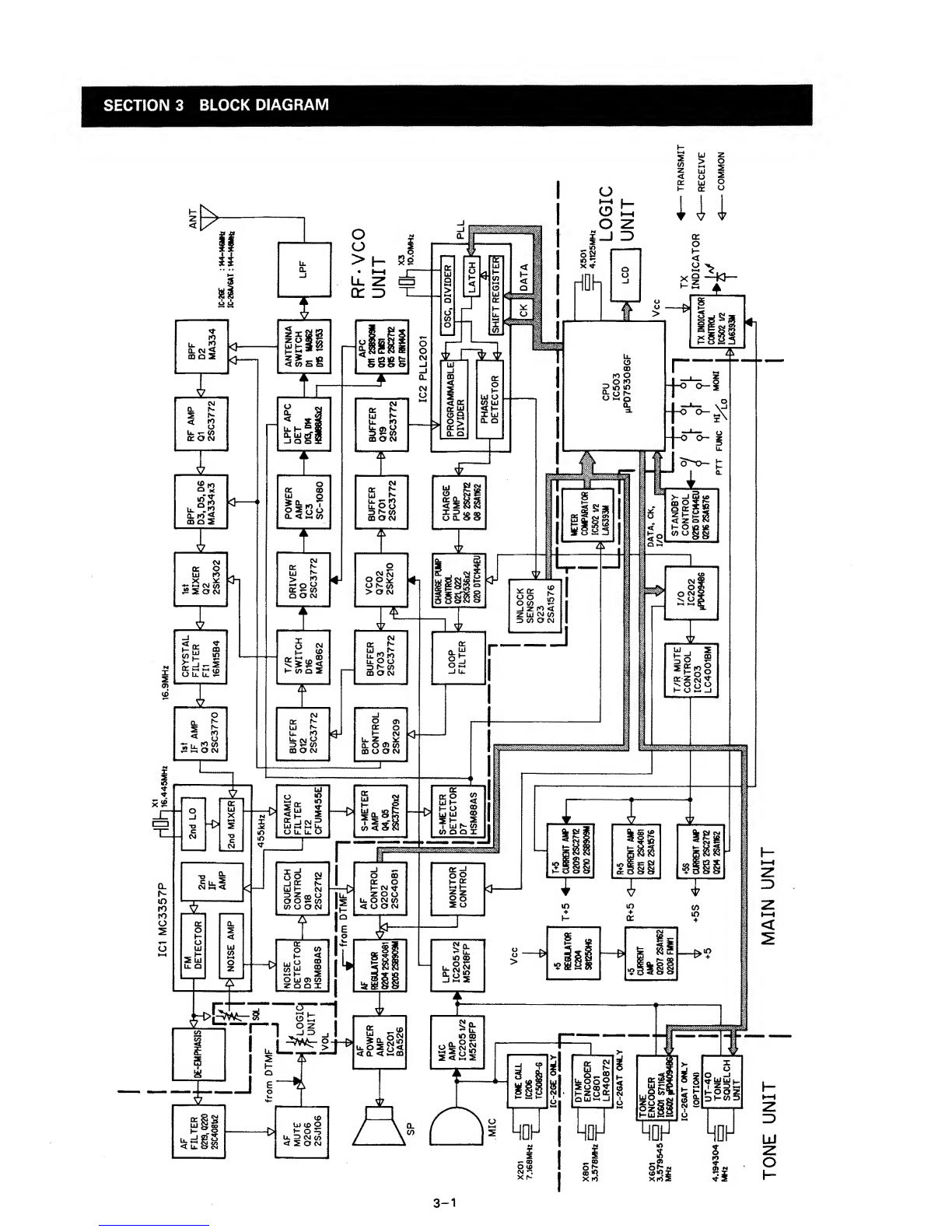
SECTION 4CIRCUIT DESCRIPTION
4-1RECEIVER CIRCUITS
(1) ANTENNA SWITCHING CIRCUIT (RF UNIT)
RF signals enter the antenna connector and pass through a
series of Chebyshev low-pass filters (LI, L2, Cl, C2, C6, C7,
C8). The signals are then applied to the antenna switching
circuit, which employs atwo-stage diode switching system
(L3, L4, C4, C5, C11, D1),
(2) RF CIRCUIT {RF UNIT)
The signals from the antenna switching circuit are ampli-
fied at Q1. Amplified signals are applied to abandpass
filter (Cl 7, C22, C25, D3, D5, D6, L6'-L8) where out-of-band
signals are suppressed. D2, D3, D5, and D6 are varactor
diodes which track the bandpass filters with the PLL lock
voltage.
(3) 1st MIXER CIRCUIT {RF UNIT)
The signals are applied to the gate of the first mixer (Q2). A
frequency oscillated in the PLL passes through the LO
switching circuit (D16), and is applied to the source of Q2.
The received signals are mixed with the PLL output to
produce the first IF of 16.9 MHz, which is picked up at L9.
{4) 1st IF AMPLIFIER {RF UNIT)
The first IF signal is applied to aset of two monolithic filters
(FI1) which determine the bandwidth (15 kHz/”3 dB) and
suppress unwanted heterodyned signals. The first IF signal
is amplified at Q3, and then applied to IC1 (pin 16) via C34.
Using XI, IC1 oscillates a2nd LO frequency of 16.445 MHz.
The second IF of 455 kHz is output from pin 3. Applied to
IC1 (pin 5), the second IF is amplified at the IC's internal
limiter amplifier. The amplified signal is applied to the
quadrature detector (IC1, pins 7, 8; X2). An AF signal Is
output from the quadrature detector through pin 9.
After passing through the ceramic filter (F12), aportion of
the second IF is applied to the S-meter amplifier (Q4, Q5).
{6) AF CIRCUIT {MAIN UNIT)
The AF signal is applied to the de-emphasis circuit (C55,
R33), and then to the AF amplifier (Q219, Q220). The
de-emphasis circuit is an integrated circuit with frequency
characteristics of -“6 dB/octave (300 Hz'-'3 kHz). Passing
through the volume control (R502), the signals are ampli-
fied by 1C201, and sent to the speaker.
{7) SQUELCH CIRCUIT {RF AND MAIN UNITS)
Aportion of the AF signal from !C1 (pin 9) is applied to pin
10 (the active filter). The SQL pot (R501) adjusts the input
level at pin 1. The active filter in IC1 amplifies noise
components of frequencies of 20 kHz and above, and
outputs the resulting signals from pin 11. The signals pass
through D9 for noise detection. If the detected noise
voltage is high, Q18 Is turned on; Q202 is turned off,
cutting off voltage buffer (Q204, Q205) output voltage. In
this way, IC201 is deactivated when the squelch is closed.
When transmitting, adecrease In Q202 voltage cuts off
voltage buffer output voltage —turning off IC201,
{5) 2nd IF AND DEMODULATOR CIRCUITS
{RF UNIT)
IC1 contains the second local oscillator, the second mixer, a
limiter amplifier, and the quadrature detector.
(8) LOCAL OSCILLATOR CIRCUIT (RF UNIT)
Q12 buffer amplifies the VCO output, which then passes
through D16 and is applied to the source of Q2.
IF CIRCUIT
AF output
to Q219
4-1