Icom IC-M72 User manual

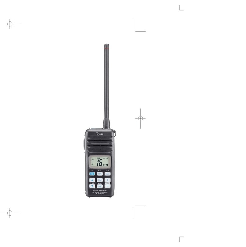
VHF MARINE TRANSCEIVER
iC-m72
S-14221MZ-C1
Jan. 2006

This service manual describes the latest service information
for the IC-M72 VHF MARINE TRANSCEIVER at the time of
publication.
Be sure to include the following four points when ordering
replacement parts:
1. 10-digit order numbers
2. Component part number and name
3. Equipment model name and unit name
4. Quantity required
<SAMPLE ORDER>
1110001811 S.IC TA7368FG IC-M72 Main unit 5 pieces
8930068440 2905 Keyboard IC-M72 Chassis 10 pieces
Addresses are provided on the inside back cover for your
convenience.
NEVER connect the transceiver to an AC outlet or to a DC
power supply that uses more than 10 V. This will ruin the
transceiver.
DO NOT reverse the polarities of the power supply when
connecting the transceiver.
DO NOT apply an RF signal of more than 20 dBm (100 mW)
to the antenna connector. This could damage the trans-
ceiver's front end.
1. Make sure a problem is internal before disassembling the transceiver.
2. DO NOT open the transceiver until the transceiver is disconnected from its power source.
3. DO NOT force any of the variable components. Turn them slowly and smoothly.
4. DO NOT short any circuits or electronic parts. An insulated turning tool MUST be used for all adjustments.
5. DO NOT keep power ON for a long time when the transceiver is defective.
6. DO NOT transmit power into a signal generator or a sweep generator.
7. ALWAYS connect a 40 dB to 50 dB attenuator between the transceiver and a deviation meter or spectrum analyzer when
using such test equipment.
8. READ the instructions of test equipment thoroughly before connecting equipment to the transceiver.
To upgrade quality, any electrical or mechanical parts
and internal circuits are subject to change without
notice or obligation.
Icom, Icom Inc. and logo are registered trademarks of Icom Incorporated (Japan) in the United States, the United
Kingdom, Germany, France, Spain, Russia and/or other countries.
INTRODUCTION
DANGER
ORDERING PARTS
REPAIR NOTES
Version Symbol Scramble AC adapter TX Power
U.S.A USA None BC-147A
6 W
USA-1 Yes
South-
east Asia
SEA None BC-147E
SEA-1 Yes
Australia AUS None BM-95V 5 W
AUS-1 Yes

TABLE OF CONTENTS
SECTION 1 SPECIFICATIONS
SECTION 2 INSIDE VIEWS
SECTION 3 DISASSEMBLY INSTRUCTIONS
SECTION 4 CIRCUIT DESCRIPTION
4 - 1 RECEIVER CIRCUITS ................................................................................................... 4 - 1
4 - 2 TRANSMITTER CIRCUITS ............................................................................................ 4 - 2
4 - 3 PLL CIRCUITS ................................................................................................................ 4 - 3
4 - 4 OTHER CIRCUITS ......................................................................................................... 4 - 4
4 - 5 POWER SUPPLY CIRCUITS ......................................................................................... 4 - 4
4 - 6 PORT ALLOCATIONS .................................................................................................... 4 - 4
SECTION 5 ADJUSTMENT PROCEDURES
5 - 1 PREPARATION ................................................................................................................ 5 - 1
5 - 2 SOFTWARE ADJUSTMENT .......................................................................................... 5 - 4
SECTION 6 PARTS LIST
SECTION 7 MECHANICAL PARTS AND DISASSEMBLY
SECTION 8 SEMICONDUCTOR INFORMATION
SECTION 9 BOARD LAYOUTS
SECTION 10 BLOCK DIAGRAM
SECTION 11 VOLTAGE DIAGRAM
SECTION 12 BC-166 INFORMATION

1 - 1
SECTION 1 SPECIFICATIONS
GENERAL
• Frequency coverage TX 156.025–157.425 MHz
RX 156.050–163.275 MHz
• Type of emission 16K0G3E
• Antenna impedance 50 Ω(nominal)
• Operating temperature range −20˚C to +60˚C; −4˚F to +140˚F
• Power supply requirement Specified Icom's battery pack only (operating volage 7.5 V DC; negative ground)
• Current drain (approx.) RX (Max. audio) 0.4 A (internal speaker)
0.2 A (external speaker)
TX
at 6 W 1.7 A
at 5 W 1.5 A
at 3 W 1.3 A
at 1 W 0.7 A
• Dimensions (projections not included) 52.5(W) × 125(H) × 30(D) mm; 2 1/16(W) × 4 29/32(H) × 1 3/16(D) in.
• Weight (approx.) 280 g; 9.9 oz. (Including BP-245)
TRANSMITTER
• Output power High 6 W (Except [AUS], [AUS-1])
5 W ([AUS], [AUS-1])
Middle 3 W
Low 1 W
• Modulation Variable reactance frequency modulation
• Max. frequency deviation ±5 kHz
• Frequency error ±10 ppm
• Spurious emissions –68 dBc typ.
• Adjacent channel power 70 dB
• Audio harmonic distortion 10% (at 60% deviation)
• Residual modulation 40 dB
• Audio frequency response +1 dB to –3 dB of 6 dB oct. from 300 Hz to 3000 Hz
• Microphone impedance 2 kΩ
RECEIVER
• Receive system Double-conversion super heterodyne
• Intermediate frequency 1st; 21.7 MHz, 2nd; 450 kHz
• Sensitivity –13 dBµ typ. (at 12 dB SINAD)
• Squelch sensitivity –9 dBµ typ. (at threshold)
• Adjacent channel selectivity 70 dB typ.
• Spurious response 70 dB typ.
• Intermodulation rejection ratio 70 dB typ.
• Hum and Noise 40 dB
• Audio frequency response +1 dB to –3 dB of –6 dB oct. from 300 Hz to 3000 Hz
• Audio output power Internal speaker 0.6 W typ. (at 10% distortion with an 8 Ωload)
External speaker 0.35 W typ. (at 10% distortion with an 8 Ωload)
• Output impedance (audio) 8 Ω
Specifications are measured in accordance with TIAIA–603.
All stated specifications are subject to change without notice or obligation.

1 - 2
r
e
bm
u
n
l
en
n
a
h
C
A
SU NAC
t
imsnar
T
e
vieceR
1
00
5
0
.
6
5
1 0
5
6
.
0
6
1
A10 0
5
0.651 050.651
20 001.651 007
.
061
30 051.651 057
.
061
A3
00
5
1
.
6
5
1 0
5
1.6
5
1
002.651 008.061
A40 00
2
.65
1002.651
052.651 0
58.
0
61
A50 A
5
00
5
2
.
6
5
1 0
5
2
.65
1
60 60 003.651 003.651
0
5
3
.
6
5
1 0
5
9
.
0
6
1
A
7
0 A
7
0053
.
6
5
1 0
5
3
.
6
5
1
8
080 0
0
4.651 004.651
90 90 054.651 054
.
651
01 0
10
0
5
.
6
5
1 0
0
5.6
5
1
1
111 0
5
5
.
6
5
1 0
5
5
.
6
5
1
21 21 00
6
.65
1006.651
31
2
*
31
1
*
056.
6
51 0
56.
6
5
1
41 41 0
0
7
.
6
5
1 0
0
7
.
6
5
1
51
2*
51
1*
0
5
7
.
6
5
105
7
.65
1
61 61 008.
6
51 008.651
71
1*
71
1*
058
.
6
5
1 0
5
8
.
6
5
1
009.6
5
1 005.161
A8
1A
81 0
0
9
.
651 009.6
5
1
)zHM(
yc
n
e
uq
e
r
F
T
N
I
1
0
20
30
40
50
60
7
0
80
90
0
1
1
1
2
1
3
1
4
1
5
1
1
*
61
7
1
8
1
r
ebmu
n
l
enn
ah
C)z
HM(
y
c
neu
qerF
A
S
UNA
C
t
im
s
n
ar
T
e
v
ie
c
e
R
A
91 A9
105
9
.
65
105
9
.
6
5
1
02 0
2
1
*
0
0
0
.7
51 0
0
6
.
1
61
12 05
0
.
7
5
105
6
.
1
6
1
A
1
2 A
1
2 0
5
0
.7
51 0
50
.
7
51
001.751 0
0
7
.
16
1
A22 A22 001
.
751 0
01
.
7
5
1
3
20
5
1
.
7
5
10
5
7.161
A32 051.751 051.751
4
242 0
02.
7
5
1 0
0
8
.
1
6
1
5
252 0
52.
7
51 0
5
8
.
1
6
1
6
262 003.751 0
09.
1
61
7
272 0
5
3
.
7
5
105
9.
16
1
82 82 0
0
4
.
7
5
1 0
0
0.2
6
1
0
6520
.
651 5
2
6.0
6
1
570
.
651 5
7
6.0
6
1
A
1
6 A
1
6 5
7
0.6
5
1 570.651
521.651 527.0
6
1
A
2
6 5
2
1
.
6
5
1 5
2
1
.
6
5
1
57
1
.65
1577
.
061
A
3
6 5
7
1
.65
1571
.
651
46 5
2
2
.
6
5
1 5
2
8
.
0
6
1
TN
I
0
2
1
2
22
3
2
4
2
5
2
6
2
7
2
8
2
0
6
16
26
36
4
6
A02 00
0
.
7
5
10
0
0
.
75
1
r
e
b
m
u
n
l
e
nn
a
hC
A6
6
)zH
M
(
yc
n
eu
qe
r
F
A6
6
1
*
A
S
UN
AC
ti
m
sn
a
r
T
e
v
i
e
c
eR
A
46 A4
65
2
2.6
5
15
2
2.6
5
1
A
5
6A5
65
72
.
6
51 5
72
.
6
51
5
2
3.6
5
15
2
9.0
6
1
7
6
2*
76 5
73.6
5
15
73.6
5
1
8
68
65
24.6
5
1 5
24.6
5
1
96 9
65
74.6
5
15
74.6
5
1
07
3*
0
7
3
*
5
25.6
5
15
25.6
5
1
17 1
75
75.6
5
1 5
75.6
5
1
2
72
75
26.
6
5
15
26.
6
5
1
37 3
757
6
.651 57
6
.651
47 47 5
27
.
6
51 5
27
.
6
51
77
1*
7
7
1*
5
78
.
6
51 5
78
.
6
51
5
2
9.6
5
1 5
2
5.1
6
1
A
8
7 A
8
75
2
9.
6
51 5
2
9.
6
51
5
79
.
651 5
75
.
1
6
1
A
97 A
97 5
79.651 5
79.6
5
1
520.751 5
26.1
6
1
A
0
8A08 520.751 5
20.751
570.751 576.161
A
1
8A18 5
7
0
.
7
5
1 5
7
0
.
7
5
1
5
2
1
.
7
5
1 5
2
7
.
1
6
1
A28 A
2
85
2
1
.
7
5
1 5
2
1
.
7
5
1
T
N
I
A
5
6
6
6
7
6
8
6
9
6
07
3*
1
7
2
7
37
4
7
7
7
8
7
9
7
08
18
2
8
5
23
.
6
51 5
23
.
6
51
A
6
6
r
eb
m
u
n
l
enn
a
h
C
A4
8
)z
H
M
(
y
c
neuqe
rF
A
S
UN
A
C
t
im
s
n
a
r
T
e
v
i
ec
e
R
A3
8A3
85
7
1
.
75
157
1
.7
5
1
4
84
85
2
2
.
7
5
15
2
8
.
1
6
1
5
85
85
7
2
.
7
5
15
7
8
.
1
6
1
A5
857
2
.
75
157
2
.
7
5
1
68 6
852
3
.
75
152
9
.
1
6
1
A
6
852
3
.
7
5
15
2
3
.
7
5
1
78 7
857
3
.
7
5
15
7
9
.
1
6
1
A
7
857
3
.
7
5
15
7
3
.7
5
1
8
88
852
4
.
7
5
15
2
0
.2
6
1
A8
85
2
4
.
75
152
4
.7
5
1
TN
I
48
58
6
8
7
8
8
8
52
2
.
75
152
2
.
7
5
1
l
e
nn
a
hc
X
W
4
)zH
M
(
y
c
n
e
uqerF
ti
m
s
n
a
r
Te
v
ie
ceR
1 y
l
n
o
X
R0
5
5
.
26
1
2 y
l
n
o
X
R00
4
.
2
6
1
3 y
l
no
X
R574.
2
61
5 y
l
no
X
R05
4
.
2
6
1
6 y
l
no
X
R00
5
.
2
6
1
7 y
l
n
o
X
R52
5
.
26
1
8 y
l
no
X
R0
5
6
.
16
1
9 y
l
no
X
R5
7
7
.
1
6
1
0
1y
l
n
o
X
R57
2
.
36
1
y
l
no
X
R52
4
.
2
6
1
1
*.
yl
nore
w
o
p
wo
L3* ylno
no
i
t
a
repoCSD
059
.
6
5
1 0
5
5
.16
1
9
1
b12 y
l
n
oxR 0
5
6
.
16
1
b
5
2 yln
o
xR 058
.
161
5
72
.
6
51 5
78
.
0
615
6
b
82 yl
n
oxR 000.261
38 5
7
1
.
7
5
1 5
7
7
.
1
6
1
3
8
b
3
8y
ln
o
x
R57
7
.
1
6
1
2
*.
r
e
w
op
hgi
h
yratne
m
o
M
:ET
O
N3
8
d
na
2
8
,1
8
,
4
6
,
16,32
,
12
,3
,s
le
nn
ahc
xe
lpm
i
ST
ON
NA
C
.
s
r
e
t
a
w
.
A
.
S
.
Un
i
c
i
lb
up
l
a
re
negeht
yb
des
u
y
l
lu
f
w
a
l
e
b
• CHANNEL LISTS

2 - 1
SECTION 2 INSIDE VIEWS
• MAIN UNIT
(Top view)
(Bottom view)
• RF UNIT
(Top view)

3 - 1
SECTION 3 DISASSEMBLY INSTRUCTIONS
2 Removing the MAIN unit
q Unscrew 5 screws D.
w Disconnect the flat cable E.
3 Removing the RF unit
q Unscrew 3 screws F.
w Unsolder 7 points G and remove the RF unit.
4 Removing the VR board and MIC board
q Remove knob I and connector cap H.
w Unscrew connector nut J and VR nut K.
e Unsolder 9 points L and remove VR board.
r Remove the VR and MIC board from the chassis.
1 Removing the chassis panel
q Unscrew 2 screws A and 4 screws B.
w Disconnect the speaker cable C and remove the
chassis from the front pannel. (The latch is come off
simultaneously)
B
A
C
D
E
F
G
HL
K
J
I

SECTION 4CIRCUIT DESCRIPTION
4-1 RECEIVE CIRCUITS
4-1-1 ANTENNA SWITCH (RF UNIT)
The received signals from the antenna connector are
passed through the antenna switch which toggles the
receive (RX) line and transmit (TX) line.
The received signals from the antenna connector are
passed through the low-pass filter (LPF; L81, L82, C80, C83
−C86, C89, C226) and the antenna switch (D52, D90 and
D353 are OFF).
While transmitting, the voltage on the T5V line is applied to
D52, D90 and D353, and these are ON. Thus the TX line is
connected to the antenna, and RX line is connected to the
GND to prevent transmit signal entering.
While receiving, no voltage is applied to D52, D90 and
D353, and these are OFF. Thus the TX line and the antenna
is disconnected to prevent received signals entering, and
RX line is disconnected from the GND and L90, L91, C90
−C92 compose a two-staged LPF which guides received
signals to the RX circuits.
The received signals are applied to the RF circuits.
4-1-2 RF CIRCUITS (RF UNIT)
The RF circuit amplifies received signals within the frequency
coverage. The received signals are filtered at the bandpass
filter (BPF) and amplified at the RF amplifier.
The received signals from the antenna switch are passed
through the two-staged tunable BPF (D92, D93, L92, L93,
C95, C97−C101) to filter out unwanted signals. The filtered
signals are applied to the RF amplifier (Q90). The amplified
signals are then applied to the 1st mixer (Q150) via another
two-staged tunable BPF (D130, D131, L96, L97, C104,
C109, C110, C112−C116).
4-1-3 1st IF CIRCUITS (RF UNIT)
The received signals are converted into the 1st IF signal,
and amplified at the 1st IF circuits.
The amplified received signals from the RF circuits are applied
to the 1st mixer (Q150), and converted into the 21.7 MHz 1st
IF signal by being mixed with the 1st local oscillator (LO)
signals from the VCO (Q21, Q22, D21−D23).
The converted 1st IF signal is passed through two 1st IF
filters (FI150, FI151) to filter out unwanted signals, and
applied to the 1st IF amplifier (Q151). The amplified 1st IF
signal is then applied to the FM IF IC (MAIN UNIT; IC170,
pin 16).
4 - 1
Mixer
Quadrature
detector
1st IF signal from the IF amplifier (RF UNIT; Q151)
16
Noise
detector
R5V
X2
1110
FM IF IC
(MAIN UNIT; IC170)
Filter
amp.
Limiter
amp.
Demodulated signals
to the AF circuits
RF UNIT
• 2ND IF AND DEMODULATOR CIRCUITS
9
(RF UNIT; IC190)
14
13
“NOISV” signal to the CPU (IC360, pin 32)
“RSSIV” signal to the CPU (IC360, pin 33)
1412
21.25 MHz
2
17
X1
21.25 MHz
8735
FI170 LPF
BPF PLL IC
(IC1)
RF UNIT
SQLO
SQLI
2NDLO
D/A
converter
ST)&SIGNAL
TOTHE&-)&)#
-!).5.)4)#PIN
1 -(Z
ST)&SIGNAL 2ECEIVEDSIGNALS
FROMTHE2&CIRCUITS
ST)&
STMIXER
1
SIGNALSFROMTHE6#/
sST)&#)2#5)43
&)&)
,0&
"0&
"0&S
4-1-4 2nd IF AND DEMODULATOR CIRCUITS
(MAIN UNIT)
The 1st IF signal is converted into the 2nd IF signal, and
demodulated.
The 1st IF signal from the 1st IF circuits is applied to the
2nd IF mixer in the FM IF IC (IC170, pin 16) and converted
into the 2nd IF signal by being mixed with the 21.25 MHz
2nd LO signal from the reference oscillator (RF UNIT; IC1,
X1) via LPF (RF UNIT; L1, C8, C9, C12).
The converted 2nd IF signal is output from pin 3, and
passed through the 2nd IF filter (FI170) to suppress
sideband noise. The filtered 2nd IF signal is applied to the
limiter amplifier (IC170, pin 5). The amplified 2nd IF signal
is FM-demodulated at the quadrature detector (IC170,
pins 10, 11) and output from pin 9. The demodulated AF
signals are applied to the AF circuits.

4-1-5 AF CIRCUITS (MAIN UNIT)
The demodulated AF signals from the demodulator circuits are
amplified and filtered in AF amplifier circuits.
The demodulated AF signals from the FM IF IC (IC170, pin 9)
are passed through the AF mute switch (IC260, pins 1, 2),
LPF (IC200, pins 8, 9) and variable register (VR BOARD;
R801) for level adjustment.
The level adjusted AF signals are passed through the
de-emphasis circuit (R286, C280, C285) to obtain −6 dB
of audio characteristic. The de-emphasized AF signals are
passed through the analog switch (IC430, pins 10, 11), and
applied to the AF power amplifier (IC401, pin 7) to obtain
0.6 W of AF output power. The power-amplified AF signals are
then output from pin 1, and applied to the internal speaker via
J251.
If an external speaker-microphone or headset is attached
to the [SP MIC] connector (MIC BOARD; J416), the
de-emphasized AF signals are passed through the analog
switch (IC430, pins 8, 9) and applied to the AF power amplifier
(IC280, pin 4) to obtain 0.2 W of AF output power. The power-
amplified AF signals are output from pin 10, and then applied
to the external speaker via the [SP MIC] connector (MIC
BOARD; J416).
4-1-6 SQUELCH CIRCUIT (MAIN UNIT)
The squelch mutes the AF output signals when no RF
signals are received. By detecting noise components in the
demodulated AF signals, the squelch circuit toggles the AF
power amplifier ON and OFF.
A portion of the demodulated AF signals from the FM IF IC
(IC170, pin 9) are applied to the D/A converter (RF UNIT;
IC190, pin 13) for level adjustment (squelch threshold
adjustment). The level-adjusted AF signals are output from pin
14, and passed through the noise filter (R174−R176, C177,
C179, C180). The filtered noise signals are then applied to
the noise amplifier in the FM IF IC (IC170, pins 7, 8) to be
amplified the noise components only.
The amplified noise components are converted into the
pulse-type signal at the noise detector section, and output
from pin 14 as the “NOISV” signal. The signal is applied
to the CPU (IC360, pin 32), and the CPU outputs “AFVS”
signal from pin 100 according to the “NOISV” signal level, to
the AF power regulator (Q230, Q231, Q401, Q540) which
toggles the AF power amplifier ON and OFF.
4-2 TRANSMIT CIRCUITS
4-2-1 MICROPHONE AMPLIFIER CIRCUITS (MAIN UNIT)
The AF signals from the microphone (MIC signals) are
filtered and level-adjusted at microphone amplifier circuits.
The AF signals from the microphone are passed through
the AF mute switch (IC430, pins 1, 2).
While an external microphone is connected to the [SP MIC]
connector (MIC BOARD; J416), the mute switch shuts out
the AF signals from the internal microphone (MC1).
AF signals from the AF mute switch (IC430, pins 1, 2) are
passed through another AF mute switch (IC430, pins 3, 4),
and passed through the pre-emphasis circuit (R253, C254) to
obtain +3 dB of characteristic. The pre-emphasized signals are
then applied to the microphone amplifier (IC200, pins 6, 7). The
amplified MIC signals are passed through AF mute switch
(IC260, pins 8, 9), and are applied to the gain controller
(Q450, Q451) whitch adjust the AF signal level (=deviation)
according to the control signals (“MIC1/2/3”) from the CPU
(IC360, pins 106/107/108).
The level adjusted MIC (MOD) signals are applied to
the limiter amplifier (IC200, pins 13, 14) which limits the
amplitude of the MIC signals to prevent over deviation. The
amplitude-limited MIC signals are then passed through the
splatter filter (IC200, pins 1, 3) which suppresses the 3 kHz
and higher audio components.
The filtered MIC signals are applied to the modulation circuit
(RF UNIT; D20).
4-2-2 MODULATION CIRCUIT (RF UNIT)
The modulation circuit modulates the VCO oscillating signal
with the AF signals from the microphone.
The MIC signals from the microphone amplifier circuits
are applied to the D20, and modulate the VCO oscillating
signal by changing the reactance of D20. The modulated
VCO output signal is buffer-amplified by Q23 and Q24, then
applied to transmit amplifiers as a transmit signal via the
TX/RX switch (D50 is ON, D51 is OFF).
4 - 2
Power
amp.
APC
amp.
Buffer
amp.
+
–
VCC
•
APC CIRCUIT
to the anntena
T5V
PCON
LOW
TXMS
from the TX/RX switch (D50)
Q53
Pre-drive
amp.
Q50
IC50
3
1
4
Q17
Q54
LPF ANT
SW
Q351
D91
D52
T5V
4-2-3 TRANSMIT AMPLIFIERS (RF UNIT)
The VCO output signal is amplified to transmit output power
level by the transmit amplifiers.
The transmit signal from the TX/RX switch (D50) is applied
to the buffer amplifier (Q50). The amplified transmit signal is
amplified to the transmit output level by the pre-driver (Q53)
and power amplifier (Q54). The power-amplified transmit
signal is passed through the TX power detector of APC circuit
(D91), antenna switch (D52, D90 and D353 are ON), TX
power detector for transmit indicator (D80) and LPF (as a
harmonic filter; L81, L82, C80, C83−C86, C89, C226) before
being applied to the antenna connector (CHASSIS; J1).
4-2-1 APC CIRCUIT (RF UNIT)
The APC (Automatic Power Control) circuit stabilizes trans-
mit output power to prevent transmit output power level change
which is caused by load mismatching or heat effect, etc,. The
APC circuit also selects transmit output power from high,
middle and low power.
The power detector circuits (D91) detects the transmit output
and converts it into DC voltage which is in proportion to the
transmit output power level. The detected voltage is applied
to the differential amplifier (IC50, pin 3). The transmit power
setting voltage “PCON” is applied to another input terminal
(pin 1) as the reference voltage.
The differential amplifier compares the detected voltage and
reference voltage, and the difference of the voltage is output
from pin 4. The output voltage controls the bias of the buffer
amplifier (Q50), pre-driver (Q53) and power amplifier (Q54)
to reduce/increase the gain of transmit amplifiers for stable
transmit output power.
The change of transmit power is carried out by the change
of reference voltage "PCON" and "LOW."
4-3 PLL CIRCUITS
4-3-1 VCO CIRCUIT (RF UNIT)
The VCO (Q21, Q22, D21−D23) generates the both of trans-
mit signal and LO signals for the 1st IF conversion. The VCO
output signals are buffer-amplified by Q23 and Q24.
While transmitting, the VCO output signal is applied to the
transmit amplifiers via TX/RX switch (D50 is ON, D51 is OFF).
While receiving, the VCO output signals are applied to the 1st
mixer (Q150) via the TX/RX switch (D50 is OFF, D51 is ON)
the BPF (L26, C122, C123, C130, C131), to be mixed with
the received signals to produce the 21.7 MHz 1st IF signal.
A portion of the VCO output is applied to the PLL IC (IC1,
pin 19) via the buffer amplifier (Q25) and LPF (L20, R20,
C20−C22).
4-3-2 PLL CIRCUIT (RF UNIT)
The PLL circuit provides stable oscillation of the transmit
frequency and receive 1st LO frequency. The PLL output
frequency is controlled by the divided ratio (N-data) from the CPU.
The buffer-amplified signals from the LPF (L20, R20, C20−
C22) are applied to the PLL IC (IC1, pin 19). The applied
signals are divided at the prescaler and programmable
counter according to the “SDATA (SDATAO)” signal from
the CPU (MAIN UNIT; IC360, pin 10). The divided signal is
phase-compared with the reference frequency signal which is
divided by reference counter, at the phase detector.
The phase difference is output from pin 13 as a pulse type
signal after being passed through the charge pump. The
output signal is converted into the DC voltage (lock voltage) by
passed through the loop filter (R8−R10, R22, C10, C11, C24,
C25). The lock voltage is applied to the variable capacitors (D22,
D23) of the VCO (Q21, Q22, D21−D23) and locked to keep
the VCO frequency constant.
If the oscillated signal drifts, its phase changes from that of
the reference frequency, causing a lock voltage change to
compensate for the drift in the VCO oscillating frequency.
4 - 3
DATA interface
Prescaler
Phase
detector
Loop
filter
Reference
counter
Programmable
counter
Charge
pump
Buffer
Q23
Buffer
Q24
Buffer
Q25 to the TX/RX switch (D50, D51)
Q22, Q37, D21–D23
VCO
LPF
to the FM IF IC
(MAIN UNIT; IC170, pin 2)
3
13
7
19
17
15
16
“PLST”
“UNLK”
• PLL CIRCUITS
“SCK”
“SDATA”
X1
4
5
PLL IC (RF UNIT; IC1)
LPF

4-4 OTHER CIRCUIT
4-4-1 VOX CIRCUIT (MAIN UNIT)
The VOX circuit toggles TX and RX automatically by detect-
ing voice signals from the microphone.
The MIC signals from the external microphone are applied
to the VOX amplifier (IC431, pins 1, 2). The amplified MIC
signals are applied to another VOX amplifier (IC431, pin 5),
and the amplified MIC signals are output from pin 7, then
rectified by D430. The rectified signal is applied to the CPU
(IC360, pin 29) as "VOXT" signal which turns the transmit
circuits ON. Then the CPU outputs "VOXM" signal from pin
117 to the AF mute switch (IC430, pin 5) to turn the AF
mute switch OFF, and the MIC signals are applied to the
pre-emphasis circuit.
4 - 4
Pin
No.
Port
Name Description
1 BEEP Outputs beep sound to the AF circuits.
4DASTB
(DAST)
Outputs strobe signal to the D/A converter (RF
UNIT; IC190, pin 6).
5PLSTB
(PLST)
Outputs PLL strobe signal to the PLL IC (RF
UNIT; IC1, pin 3).
11 SCLK
(SCK)
Outputs serial crock signal to the PLL IC (RF
UNIT; IC1, pin 4), D/A converter (RF UNIT;
IC190, pin 7).
12 V5VS
Outputs V5V regulator (Q220) control signal.
"High"= While power save mode (The VCO
(Q21, Q22, D21−D23) is not activated).
13 T5VS
Outputs T5V regulator (RF UNIT; Q222) control
signal.
"Low"= While transmitting.
"High"= While receiving or power save mode.
14 LCDS
Outputs LCD contrast select signal.
"Low"= While "Bright" is selected.
"High"= While "Dark" is selected.
15 LEDS
Outputs backlight LED (DS240−DS243, DS250−
DS253) control signal to the LED driver (Q240).
"High"= While the backlight is ON.
25 RES Input port for reset signal from the reset IC
(IC341, pin 1).
27†WDECV Input port for demodulated weather alart (WX)
signal from the AF circuits.
28 EXDET Input port for external connect detect signal.
29 VOXT Input port for audio detect signal from the VOX
amplifier (IC431, pin 7) for the VOX operation.
30 BATTV Input port for remaining battery power.
31 TDETV Input port for power level detect signal from the
transmit power detector (RF UNIT; D80).
32 NOISV Inputo port for the noise level from the FM IF IC
(IC170, pin 14).
33 RSSIV Input port for RSSI signal from the FM IF IC
(IC170, pin 12).
34 LOINV Input port for VCO (Q21, Q22, D21−D23) lock
voltage.
35 TEMPV Input port for temperture detection.
36 WET Input port for leaking detection signal.
93 ESCK Outputs serial crock signal to the EEPROM
(IC340, pin 6).
94 ESDA Outputs serial data to the EEPROM (IC340, pin 5).
95 R5VS
Output R5V line control signal to the R5V
regulator (Q221).
"High"= While receiving.
96 EXPTT Input port for external PTT switch.
"High"= While the external PTT switch is pushed.
97 TXMS
Outputs transmit mute signal to the transmit
mute switch (Q351).
"High"= While transmitting.
98 DETMS
Outputs mute signal to the AF mute switch
(IC260, pin 13).
"High"= While the squelch is open.
100 AFVS
Outputs AF power amplifier power supply
switch control signal.
"High"= While the audio is emitted from the internal
speaker (CHASSIS; SP1) or external speaker.
102 PTTIN Input port for [PTT] switch. (RF UNIT; S250)
"High": While [PTT] switch is pushed.
Line
name Description
VCC The same voltage as attached battery pack.
CPU5V
Common 5 V converted from VCC line at the
CPU5V regulator (IC220).
The converted voltage is applied to the CPU
(IC360), Reset IC (IC341), EEPROM (IC340), etc.
5V
Common 5 V converted from VCC line at the 5V
regulator (Q223−Q225) controlled by "M5VS" signal
from CPU (IC360, pin 101).
The converted voltage is applied to the backlight
LED'S (DS240−DS243, DS250−DS253), D/A con-
verter (RF UNIT; IC190), PLL IC (RF UNIT; IC1), etc.
V5V
Common 5 V converted from VCC line at the V5V
regulator (RF UNIT; Q220).
The converted voltage is applied to the VCO (RF
UNIT; Q21, Q22, D21−D23)
R5V
Receive 5 V controlled by R5V regulator (Q221)
using "R5VS" signal from the CPU (IC360, pin 95).
The voltage is applied to the receive circuits (RF
UNIT; 1st mixer (Q150), 1st IF amplifier (Q151),
RF amplifier (Q90), etc.).
T5V
Transmit 5 V controlled by T5V regulator (RF UNIT;
Q222) using "T5VS" signal from the CPU (IC360,
pin 13).
The controlled voltage is applied to the transmit
circuits (RF UNIT; differential amplifier (IC50), pre-
driver (Q53), power amplifier (Q54), microphone
amplifier (IC8), etc.).
4-5 POWER SUPPLY CIRCUITS
(MAIN UNIT AND RF UNIT)
4-6 PORT ALLOCATIONS
4-6-1 CPU (MAIN UNIT; IC360)
†; ([USA], [USA-01] only)

Pin
No.
Port
Name Description
104 BTYPE Input port for battery type detect signal.
105 PTTM
Outputs MIC mute signal to the AF mute switch
(IC430, pin 13).
"High": While transmitting.
"Low": While transmitting in VOX operation.
106 MIC1/
SPCTRL
• While transmitting.
Outputs microphone sensitivity control signal to
the MIC gain controller (Q450, Q451).
(The microphone sensitivity is determinded by
the combination of "MIC1−MIC3".)
• While recseiving.
Outputs AF line switching signal to the analog
switch (IC430, pins 6, 12).
107 MIC2/
AFVCTRL
• While transmitting.
Outputs microphone sensitivity control signal
to the MIC gain controller (Q450, Q451).
• While recseiving.
Outputs AF power amplifier (IC280 or IC401)
bias change signal to the AF amplifier power
supply circuit (Q230, Q231, Q401, Q540).
108 MIC3/
BPCTRL
• While transmitting.
Outputs microphone sensitivity control signal to
the MIC gain controller (Q450, Q451).
• While recseiving.
Outputs AquaQuake function activate signal.
"Low": AquaQuake function is activated.
109 SQL Input port for [SQL] key (RF UNIT; S250).
"Low": While [SQL] is pushed.
110 UP Input port for [ ] key (MAIN UNIT; S321).
"Low": When [ ] key is pushed.
111 DOWN Input port for [ ] key (MAIN UNIT; S322).
"Low": When [ ] key is pushed.
112 CH/WX Input port for [CH/WX] key (MAIN UNIT; S324).
"Low": When [CH/WX] key is pushed.
113 16 Input port for [16] key (MAIN UNIT; S320).
"Low": When [16] key is pushed.
114 SCAN Input port for [SCAN] key (MAIN UNIT; S324).
"Low": When [SCAN] key is pushed.
115 H/L Input port for [H/L] key (MAIN UNIT; S329).
"Low": When [H/L] is pushed.
117 VOXM
Outputs MIC mute signal to the AF mute switch
(IC430, pin 5).
"High": While transmitting.
119 UNLK
Input port for PLL unlock signal ("UNLK") from
the PLL IC (IC1, pin 7).
"High": While the PLL is unlocked.
4 - 5
4-6-2 D/A CONVERTER (RF UNIT; IC190)
Pin
No.
Port
Name Description
2 MODC Outputs deviation adjust signal.
3 FCON Outputs reference frequency adjust signal.
10 PCON Outputs transmit power setting voltage.
11 ATTS
Outputs attenuator (RF UNIT; D94) switching
signal.
"High"=The attenuator (RF UNIT; D94) is activated.
15 LOW
Outputs transmit power setting signal.
"High"=TX power [High] or [Mid] is selected.
"Low"=TX power [LOW] is selected.
22 T2CON Outputs center frequency tracking voltage to the
BPF (RF UNIT; D131, L97, C112−C116).
23 T1CON
Outputs center frequency tracking voltage to
the BPF'S (RF UNIT; D130, L96, C104, C109,
C110).
4-6-1 CPU (MAIN UNIT; IC360)-continued

5 - 1
SECTION 5 ADJUSTMENT PROCEDURES
EQUIPMENT GRADE AND RANGE EQUIPMENT GRADE AND RANGE
RF power meter
(terminated type)
Measuring range : 0.1–10 W
Frequency range : 100–300 MHz
Impedance : 50 Ω
SWR : Less than 1.2 : 1
Standard signal
generator (SSG) Frequency range : 0.1–300 MHz
Output level : 0.1 µV to 32 mV
(–127 to –17 dBm)
Frequency counter
Frequency range : 0.1–300 MHz
Frequency accuracy: ±1 ppm or better
Sensitivity : 100 mV or better
Oscilloscope Frequency range : DC–20 MHz
Measuring range : 0.01–20 V
FM deviation meter Frequency range : 30–300 MHz
Measuring range : 0 to ±10 kHz AC millivoltmeter Measuring range : 1 mV to 10 V
Audio generator
Frequency range : 300–3000 Hz
Output level : 1–500 mV
Impedance : 600 Ω
External speaker Input impedance : 8 Ω
Capacity : More than 1 W
Attenuator Power attenuation : 30 dB or more
Capacity : More than 10 W
5-1 PREPARATION
REQUIRED TEST EQUIPMENTS
When adjusting IC-M72, the optional CS-M72 ADJ ADJUSTMENT SOFTWARE (Rev. 1.0 or later), OPC-478 (RS-232 type) or OPC-
478U (USB type) CLONING CABLE, OPC-1028 and JIG cable (see page 5-2) are required.
Microsoft and Windows are registered trademarks of
Microsoft Corporation in the U.S.A. and other countries.
STARTING SOFTWARE ADJUSTMENT
(1) Connect IC-M72 and a PC with OPC-478/U,
OPC-1028 and JIG CABLE.
(2) Turn the transceiver ON.
(3) Boot up Windows®, and click the program group 'CS-M72
ADJ’ in the ‘Programs’ folder of the [Start] menu,
then CS-M72 ADJ’s window appears.
(4) Click ‘Adjust’ on the CS-M72’s window, then IC-M72’s
up-to-date condition appears.
(5) Set or modify adjustment value as specified.
CAUTION!: BACK UP the originally programmed memory
data in the transceiver before programming
the adjustment frequencies.
When program the adjustment frequencies
into the transceiver, the transceiver’s memory
data will be overwritten and lose original
memory data at the same time.

5 - 2
• CONNECTION
FM
deviation meter
SINAD meter
Speaker (8 Ω)
Audio generator
AC millivoltmeter
to the antenna connector
Attenuator
30 dB or more
RF power meter
0.1–10 W/50 Ω
Frequency
counter
Standard signal generator
0.1 µV to 32 mV
(–127 dBm to –17 dBm)
DO NOT transmit while
an SSG is connected to
the antenna connector.
To CLONE line
(BLACK)
To MIC line
(WHITE)
To SP line
(RED)
IC-M72
OPC-478/U WHITE (EXTMIC)
(MIC line)
(SP line)
BLACK (EXDET)
SHIELD (SPG)
(CLONE line)
OPC-1028
RED (AFOUT)
To audio generator/AC millivoltmeter
To SINAD meter/speaker
JIG cable
PC
to USB port
to RS-232C port
OPC-478 (RS-232C type)
OPC-478U (USB type)
OPC-1028
PTT33 k
Ω

5 - 3
• PC SCREEN EXAMPLE
NOTE: The above screen is an example.
Each transceiver has its own specific values for each setting.
q: Adjustment condition
w: Reference frequency
e: Transmit output power
r: FM deviation
t: Receive sensitivity (Automaticaly)
y: Receive sensitivity (Manualy)
u: Squelch level
i: VOX
q
w
e
i
r
t
u
y
I/O check button

5 - 4
ADJUSTMENT ADJUSTMENT CONDITION
MEASUREMENT
VALUE
UNIT OPERATION
PLL LOCK
VOLTAGE
(Verify)
1 • Operating CH. : 16
• Receiving
PC
screen
Click the "I/O check button" on
the CS-M72 ADJ's screen (see
page 5-3) to open the I/O check
window as below.
1.65–2.65 V
(Verify)
2 • Operating CH. : 16
• Connect a dummy load or RF power
meter to the antenna connector.
• Transmitting
1.75–2.75 V
(Verify)
REFERENCE
FREQUENCY
[Ref Freq]
1 • Operating CH. : 16
• Connect the RF power meter or a 50 Ω
dummy load to the antenna connector.
• Transmitting
Top
Panel
Loosely couple the frequency
counter to the antenna conector.
156.8000 MHz
5-2 SOFTWARE ADJUSTMENT (FREQUENCY)
Select the adjustment item with [↑] / [↓] keys, then set the value with [←] / [→] keys on the connected PC.
PLL LOCK VOLTAGE
NOTE: The above screen is an example.
Each transceiver has its own specific values.

5 - 5
ADJUSTMENT ADJUSTMENT CONDITION MEASUREMENT VALUE
UNIT OPERATION
RECEIVE
SENSITIVITY
[BPF T1]
[BPF T2]
1 • Operating CH.: 16
• Connect the standard signal
generator to the antenna connector
and set as;
Frequency : 156.8000 MHz
Level : +20 dBµ* (–87 dBm)
Modulation : 1 kHz
Deviation : ±3.0 kHz
• Receiving
Top
pannel
Connect the distortion meter
with an 8 Ωload to the [MIC/
SP] jack through the JIG
cable.
Minimum distortion level
CONVENIENT:
RECEIVE SENSITIVITY can be adjusted automatically.
1. Put the cursor on the [BPF ALL Sweep] on the CS-M72 ADJ's screen and push the [ENTER] key.
2. The connected PC tunes BPF T1 and T2 to peak level automaticaly.
or
1. Put the cursor on the one of BPF T1 and T2 as desired.
2. Push the [ENTER] key to start tuning.
3. Repeat 1 and 2 to perform additional BPF tuning.
SQUELCH
LEVEL
[NOISE]
Need to adjust "SQUELCH LEVEL" after "RECEIVE SENSITIVITY" is adjusted. Otherwise, "SQUELCH
LEVEL" will not be adjusted properly.
1 • Operating CH. : 16
• Connect the standard signal
generator to the antenna connector
and set as;
Frequency : 156.8000 MHz
Level : –4 dBµ* (–111 dBm)
Modulation : 1 kHz
Deviation
: ±3.0 kHz
• Receiving
Top
panel
Push the [ENTER] key on the
keyboad of the connected PC.
Automatic
adjustment
TRANSMIT
OUTPUT POWER
[RF Power (High)]
1 • Operating CH. : 16
• RF power : High
• Transmitting
Top
panel
Connect the RF power meter
to the antenna connector.
5.6 W
(Except [AUS], [AUS-1])
4.7 W
([AUS], [AUS-1])
[RF Power (Middle)] 2 • Operating CH. : 16
• RF power : Middle
• Transmitting
3.0 W
[RF Power (Low)] 3 • Operating CH. : 16
• RF power : Low
• Transmitting
0.75 W
FM DEVIATION
[MOD]
1 • Operating CH. : 16
• Set the FM deviation meter as;
HPF : OFF
LPF : 20 kHz
De-emphasis : OFF
Detector : (P–P)/2
• Connect the audio generator to
the [MIC/SP] jack through OPC-973
and set as;
Frequency : 1 kHz
Level : 25 mV rms
• Transmitting
Top
panel
Connect the FM deviation
meter to the antenna con-
nector through the attenuator.
±4.30–4.40 kHz
VOX
[VOX]
1 • Operating CH. : 16
• Set to VOX mode.
(Push and hold [ ], then push
[H/L•LOCK])
• No audio applied to the [SP MIC] jack.
PC
screen
Push the [ENTER] key on the
keyboad of the connected PC.
Automatic
adjustment
5-3 SOFTWARE ADJUSTMENT (RECEIVE AND TRANSMIT)
Select the adjustment item with [↑] / [↓] keys, then set the value with [←] / [→] keys on the connected PC.
NOTE: "RECEIVE SENSITIVITY" should be adjusted before "SQUELCH LEVEL," or "SQUELCH LEVEL" will not be adjusted properly.
*The output level of the standard signal generator (SSG) is indicated as the SSG's open circuit.

6 - 1
SECTION 6 PARTS LIST
M.=Mounted side (T: Mounted on the Top side, B: Mounted on the Bottom side)
[MAIN UNIT]
REF ORDER DESCRIPTION M. H/V
NO. NO.
LOCATION
IC170 1110003201 S.IC TA31136FNG (EL) B 52/32.6
IC200 1110003780 S.IC NJM2902V-TE1 B 25.1/32.2
IC220 1110005350 S.IC NJM2870F05-TE1 B 22.8/12.3
IC260 1130011770 S.IC CD4066BPWR B 32.7/30.8
IC280 1110001810 S.IC TA7368F (ER) [USA], [SEA] B 15.9/12.4
1110001811 S.IC TA7368FG (5 ER)
[AUS], [scramble] B 15.9/12.4
IC340 1130012430 S.IC S-24CS64A0I-T8T1G B 67.3/36.2
IC341 1110005770 S.IC S-80942CNMC-G9C-T2 [AUS] B 72.4/39.2
1110005771 S.IC S-80942CNMC-G9CT2G
Except [AUS] B 72.4/39.2
IC360 1140010620 S.IC µPD78F0338GC-9EB [AUS] B 74.2/14.6
1140013300 S.IC µPD78F0338GC-9EB-A
Except [AUS] B 74.2/14.6
IC401 1110002420 S.IC NJM2073M-TE1 B 19.7/20.2
IC410 1130009900 S.IC FX214L2/TR [scramble] only B 56/9.5
IC411 1110006380 S.IC LM2904PWR [scramble] only B 34.4/18.7
IC412 1130007991 S.IC TC3W03FU (TE12L F)
[scramble] only B 63.5/8.2
IC430 1130011770 S.IC CD4066BPWR B 16.7/36.5
IC431 1110006380 S.IC LM2904PWR B 12/3.1
Q221 1510001090 S.TR KTA2015Y-RTK/P B 28.4/19.4
Q223 1590003290 S.TR UNR9213J-(TX) B 25.7/11.6
Q224 1590001190 S.TR XP6501-(TX) AB B 25.7/16
Q225 1520000840 S.TR KTA1664Y-RTF/P B 28.6/13.6
Q230 1550000090 S.FET RSQ035P03TR B 29.4/9.2
Q231 1590001190 S.TR XP6501-(TX) AB B 33/8.2
Q240 1590003290 S.TR UNR9213J-(TX) B 84.7/35.9
Q250 1590003380 S.TR UNR9111J-(TX) B 10.2/37.1
Q350 1590003270 S.TR UNR9210J-(TX) B 78.9/37.8
Q351 1590003550 S.TR XP4313 (TX) B 75.5/39.9
Q400 1590003290 S.TR UNR9213J-(TX) B 13.3/33.2
Q401 1590003290 S.TR UNR9213J-(TX) B 34.2/5.4
Q430 1590003380 S.TR UNR9111J-(TX) B 10.1/35
Q450 1590001770 S.TR XP1213 (TX) B 25.6/23.9
Q451 1590003290 S.TR UNR9213J-(TX) B 27.9/23.9
Q470 1590003290 S.TR UNR9213J-(TX) B 14.2/25.4
Q500 1590003290 S.TR UNR9213J-(TX) B 80.1/4.6
Q540 1590003230 S.TR UNR9113J-(TX) B 35.3/7.7
Q541 1590003290 S.TR UNR9213J-(TX) [scramble] only B 66.8/1.3
D350 1750001180 S.DIO KDS122 RTK/P B 81.3/37.8
D430 1790001250 S.DIO MA2S111-(TX) B 9.1/6.1
FI170 2020001530 CER CFWLB450KFFA-B0 [AUS] B 59/32.9
2020002170 S.CER ELFY450E Except [AUS] B 59/32.9
X170 6070000190 S.DCR CDBCB450KCAY24-R0 B 54.1/21.5
X410 6050008910 XTL AT-38 (4.000 MHz) [scramble] only
X480 6050011500 S.XTL CR-739 (9.8304 MHz) B 81.9/29.2
R170 7030009280 S.RES ERJ2GEJ 391 X (390) B 50.3/24.6
R171 7030007570 S.RES ERJ2GEJ 122 X (1.2 k)B 50.3/26.2
R172 7030005000 S.RES ERJ2GEJ 471 X (470) B 54/27.1
R173 7030005030 S.RES ERJ2GEJ 152 X (1.5 k)B 50.7/36.9
R174 7030006610 S.RES ERJ2GEJ 394 X (390 k)B 53.8/36.9
R175 7030005600 S.RES ERJ2GEJ 273 X (27 k)B 54/38.1
R176 7030005120 S.RES ERJ2GEJ 102 X (1 k)B 52.2/38.9
R201 7030005050 S.RES ERJ2GEJ 103 X (10 k)B 28/29.1
R202 7030005090 S.RES ERJ2GEJ 104 X (100 k)B 29.2/29.1
R203 7030003810 S.RES ERJ3GEYJ 125 V (1.2 M)B 26.5/27.5
R204 7030005040 S.RES ERJ2GEJ 472 X (4.7 k)B 25.2/28.9
R205 7030005210 S.RES ERJ2GEJ 822 X (8.2 k)B 22.9/24.6
R206 7030008290 S.RES ERJ2GEJ 183 X (18 k)B 22.4/26.9
R207 7030005600 S.RES ERJ2GEJ 273 X (27 k)B 24.7/27.9
R212 7030005030 S.RES ERJ2GEJ 152 X (1.5 k)B 21.5/28.3
R213 7030005070 S.RES ERJ2GEJ 683 X (68 k)B 21.1/27
R214 7030007340 S.RES ERJ2GEJ 153 X (15 k)B 19.8/27.7
R222 7030005050 S.RES ERJ2GEJ 103 X (10 k)B 26.8/17.8
R223 7030005040 S.RES ERJ2GEJ 472 X (4.7 k)B 28.4/17.6
R226 7030007290 S.RES ERJ2GEJ 222 X (2.2 k)B 25/13.4
R227 7030005050 S.RES ERJ2GEJ 103 X (10 k)B 31.7/13.1
R228 7030005220 S.RES ERJ2GEJ 223 X (22 k)B 23.8/16
R230 7030005600 S.RES ERJ2GEJ 273 X (27 k)B 30.7/6.2
R231 7030005160 S.RES ERJ2GEJ 105 X (1 M)B 32.7/5.9
R232 7030005120 S.RES ERJ2GEJ 102 X (1 k)B 32.7/11.4
R233 7030007290 S.RES ERJ2GEJ 222 X (2.2 k)B 33.1/10.1
S.=Surface mount
[MAIN UNIT]
REF ORDER DESCRIPTION M. H/V
NO. NO.
LOCATION
R234 7030007300 S.RES ERJ2GEJ 332 X (3.3 k)B 34.8/9.7
R235 7030005930 S.RES ERJ3GEYF 334 V (330 k)B 32.8/13.5
R236 7030008090 S.RES ERJ3EKF 1503 V (150 k)B 31.8/16
R240 7030007280 S.RES ERJ2GEJ 331 X (330) [AUS] B 65.4/4.2
7030008280 S.RES ERJ2GEJ 271 X (270)
Except [AUS] B 65.4/4.2
R241 7030005010 S.RES ERJ2GEJ 681 X (680) T 38.9/21.3
R243 7030007280 S.RES ERJ2GEJ 331 X (330) [AUS] B 52.8/40.9
7030008280 S.RES ERJ2GEJ 271 X (270)
Except [AUS] B 52.8/40.9
R244 7030005010 S.RES ERJ2GEJ 681 X (680) T 23.6/21.3
R245 7030005090 S.RES ERJ2GEJ 104 X (100 k)B 17.7/7
R250 7030005090 S.RES ERJ2GEJ 104 X (100 k)[AUS] B 7.6/35.2
7030005700 S.RES ERJ2GEJ 274 X (270 k)
Except [AUS] B 7.6/35.2
R251 7030005000 S.RES ERJ2GEJ 471 X (470) B 12.1/36.3
R252 7030005060 S.RES ERJ2GEJ 333 X (33 k)B 9.5/39.6
R253 7030007290 S.RES ERJ2GEJ 222 X (2.2 k)B 21/35.9
R255 7030008300 S.RES ERJ2GEJ 184 X (180 k)B 21.9/35.2
R256 7030008290 S.RES ERJ2GEJ 183 X (18 k)B 20/36.2
R257 7030005040 S.RES ERJ2GEJ 472 X (4.7 k)B 22.3/36.4
R258 7030005040 S.RES ERJ2GEJ 472 X (4.7 k)B 24.7/35.5
R259 7030005720 S.RES ERJ2GEJ 563 X (56 k)B 23.1/35.5
R260 7030005671 S.RES ERA3YKD 393V (39 k)B 20.3/7.5
R261 7030009591 S.RES ERA3YED 472V (4.7 k)B 18.9/7.5
R262 7030006601 S.RES ERA3YED 272V (2.7 k)B 22.1/6.1
R263 7030005090 S.RES ERJ2GEJ 104 X (100 k)B 35.7/27.6
R264 7030005090 S.RES ERJ2GEJ 104 X (100 k)B 30.7/26.5
R265 7030005090 S.RES ERJ2GEJ 104 X (100 k)B 35.3/36
R271 7030005720 S.RES ERJ2GEJ 563 X (56 k)B 33.2/36.6
R272 7030005700 S.RES ERJ2GEJ 274 X (270 k)B 31.8/36.5
R273 7030005240 S.RES ERJ2GEJ 473 X (47 k)B 31.8/35.6
R274 7030006610 S.RES ERJ2GEJ 394 X (390 k)B 19/24.3
R275 7030005050 S.RES ERJ2GEJ 103 X (10 k)B 20.3/24
R276 7030008300 S.RES ERJ2GEJ 184 X (180 k)B 17.7/24.4
R277 7030005090 S.RES ERJ2GEJ 104 X (100 k)B 29.4/32.3
R278 7030005120 S.RES ERJ2GEJ 102 X (1 k)B 31.2/37.7
R279 7030005030 S.RES ERJ2GEJ 152 X (1.5 k)B 28.5/35.1
R283 7030007260 S.RES ERJ2GEJ 330 X (33) B 19.3/9.3
R284 7030005530 S.RES ERJ2GEJ 100 X (10) B 12.3/8.6
R286 7030005050 S.RES ERJ2GEJ 103 X (10 k)B 17.8/28.6
R288 7030005110 S.RES ERJ2GEJ 224 X (220 k)B 18.8/25.5
R289 7030005090 S.RES ERJ2GEJ 104 X (100 k)B 17.5/26.3
R290 7030005050 S.RES ERJ2GEJ 103 X (10 k)B 16.2/25.9
R300 7030005290 S.RES ERJ2GEJ 682 X (6.8 k)B 24/25.9
R340 7030005050 S.RES ERJ2GEJ 103 X (10 k)B 72/35.9
R341 7030005050 S.RES ERJ2GEJ 103 X (10 k)B 72/36.8
R343 7030005050 S.RES ERJ2GEJ 103 X (10 k)B 73.2/36.6
R350 7030005170 S.RES ERJ2GEJ 474 X (470 k)B 52.3/2.5
R351 7030005120 S.RES ERJ2GEJ 102 X (1 k)B 77.8/36.2
R352 7030007340 S.RES ERJ2GEJ 153 X (15 k)B 78.6/35.3
R353 7030005120 S.RES ERJ2GEJ 102 X (1 k)B 77.4/37.4
R354 7030005090 S.RES ERJ2GEJ 104 X (100 k)B 76.2/37.3
R355 7030005090 S.RES ERJ2GEJ 104 X (100 k)B 76.2/35.9
R356 7030005080 S.RES ERJ2GEJ 823 X (82 k)B 77.4/39
R357 7030005240 S.RES ERJ2GEJ 473 X (47 k)B 75/38.2
R358 7030005050 S.RES ERJ2GEJ 103 X (10 k)
Except [AUS] B 61.8/39.5
7030010040 S.RES ERJ2GEJ-JPW [AUS] B 61.8/39.5
R359 7030005090 S.RES ERJ2GEJ 104 X (100 k)B 79.7/36.2
R375 7030005290 S.RES ERJ2GEJ 682 X (6.8 k)B 20/39.7
R376 7030005090 S.RES ERJ2GEJ 104 X (100 k)B 24/26.9
R377 7030005080 S.RES ERJ2GEJ 823 X (82 k)B 23.1/27.9
R378 7030005080 S.RES ERJ2GEJ 823 X (82 k)B 21.3/29.3
R379 7030005080 S.RES ERJ2GEJ 823 X (82 k)B 19.9/30.8
R393 7030005090 S.RES ERJ2GEJ 104 X (100 k)B 32.6/26
R394 7030005090 S.RES ERJ2GEJ 104 X (100 k)B 34.1/36
R395 7030005090 S.RES ERJ2GEJ 104 X (100 k)
[scramble] only B 34.7/26.5
R400 7030005090 S.RES ERJ2GEJ 104 X (100 k)B 15.2/31.3
R401 7030005050 S.RES ERJ2GEJ 103 X (10 k)B 16.1/24.1
R402 7030005530 S.RES ERJ2GEJ 100 X (10) B 15.2/18.8
R403 7030005170 S.RES ERJ2GEJ 474 X (470 k)B 16.4/31.8
R410 7030005050 S.RES ERJ2GEJ 103 X (10 k)
[scramble] only B 32.7/23
R411 7030005720 S.RES ERJ2GEJ 563 X (56 k)
[scramble] only B 34.3/23
R412 7030005090 S.RES ERJ2GEJ 104 X (100 k)
[scramble] only B 32/20.2
R413 7030008290 S.RES ERJ2GEJ 183 X (18 k)
[scramble] only B 34.6/13.5
R414 7030007300 S.RES ERJ2GEJ 332 X (3.3 k)
[scramble] only B 34.6/14.4
[scramble]=[USA-1], [SEA-1], [AUS-1]

6 - 2
M.=Mounted side (T: Mounted on the Top side, B: Mounted on the Bottom side)
S.=Surface mount
[MAIN UNIT]
REF ORDER DESCRIPTION M. H/V
NO. NO.
LOCATION
R415 7030005090 S.RES ERJ2GEJ 104 X (100 k)
[scramble] only B 32/18.6
R416 7030005160 S.RES ERJ2GEJ 105 X (1 M)
[scramble] only B 63.8/4.2
R417 7030005120 S.RES ERJ2GEJ 102 X (1 k)
[scramble] only B 62.9/5.1
R419 7030005040 S.RES ERJ2GEJ 472 X (4.7 k)
[scramble] only B 36.8/20
R430 7030005090 S.RES ERJ2GEJ 104 X (100 k)B 10.2/33
R431 7030005090 S.RES ERJ2GEJ 104 X (100 k)B 11.7/33.9
R432 7030005090 S.RES ERJ2GEJ 104 X (100 k)B 14.8/32.2
R433 7030007340 S.RES ERJ2GEJ 153 X (15 k)B 11.8/6.8
R434 7030005230 S.RES ERJ2GEJ 334 X (330 k)B 10.5/5.5
R435 7030008400 S.RES ERJ2GEJ 182 X (1.8 k)B 6.7/2.7
R436 7030006610 S.RES ERJ2GEJ 394 X (390 k)B 7.7/2.7
R437 7030005220 S.RES ERJ2GEJ 223 X (22 k)B 7.7/4.3
R438 7030007310 S.RES ERJ2GEJ 155 X (1.5 M)B 7.7/5.6
R439 7030005040 S.RES ERJ2GEJ 472 X (4.7 k)B 13.8/6.8
R440 7030005210 S.RES ERJ2GEJ 822 X (8.2 k)B 13.7/5.5
R441 7030005090 S.RES ERJ2GEJ 104 X (100 k)B 16.3/6.7
R442 7030005040 S.RES ERJ2GEJ 472 X (4.7 k)B 12.1/5.5
R450 7030008290 S.RES ERJ2GEJ 183 X (18 k)B 26.4/25.8
R451 7030005210 S.RES ERJ2GEJ 822 X (8.2 k)B 28/25.4
R452 7030008410 S.RES ERJ2GEJ 392 X (3.9 k)B 29.3/25.4
R453 7030005120 S.RES ERJ2GEJ 102 X (1 k)B 28/26.3
R454 7030005170 S.RES ERJ2GEJ 474 X (470 k)
Except [AUS] only B 29.2/28.2
R481 7030005160 S.RES ERJ2GEJ 105 X (1 M)B 85/25.8
R483 7030005530 S.RES ERJ2GEJ 100 X (10) B 85/27.4
R489 7030005050 S.RES ERJ2GEJ 103 X (10 k)B 72.9/25.3
R491 7030005050 S.RES ERJ2GEJ 103 X (10 k)B 78.3/24.9
R493 7030005050 S.RES ERJ2GEJ 103 X (10 k)B 76.4/25.5
R495 7030005050 S.RES ERJ2GEJ 103 X (10 k)B 78.3/23.9
R496 7030005050 S.RES ERJ2GEJ 103 X (10 k)B 79.5/22.7
R497 7030005050 S.RES ERJ2GEJ 103 X (10 k)B 80.5/21.5
R498 7030009150 S.RES ERJ2GEJ 824 X (820 k)B 79.3/6.3
R499 7030007310 S.RES ERJ2GEJ 155 X (1.5 M)B 80.9/7.1
R500 7030007060 S.RES ERJ2GEJ 684X (680 k)B 82/5.9
R501 7030008300 S.RES ERJ2GEJ 184 X (180 k)B 81.1/5.9
R502 7030010040 S.RES ERJ2GEJ-JPW [scramble] only B 72.9/26.2
R505 7030005090 S.RES ERJ2GEJ 104 X (100 k)B 64.8/18.6
R512 7030005120 S.RES ERJ2GEJ 102 X (1 k)
[scramble] only B 66/3
R520 7030010040 S.RES ERJ2GEJ-JPW B 10.4/38.9
R521 7030009140 S.RES ERJ2GEJ 272 X (2.7 k)
Except [AUS] B 11.3/38.9
7030010040 S.RES ERJ2GEJ-JPW [AUS] B 11.3/38.9
R540 7030005700 S.RES ERJ2GEJ 274 X (270 k)B 27.2/10.2
R541 7030005050 S.RES ERJ2GEJ 103 X (10 k)B 27.8/6.9
C160 4030018240 S.CER ECJ0EB1E562K B 50.3/23
C170 4030017460 S.CER ECJ0EB1E102K B 51.3/38.1
C171 4030017680 S.CER ECJ0EC1H820J B 52.3/27.9
C174 4030017460 S.CER ECJ0EB1E102K B 54.6/28.3
C175 4030017460 S.CER ECJ0EB1E102K B 56.1/26.3
C176 4030017460 S.CER ECJ0EB1E102K B 54.9/27.1
C177 4030016930 S.CER ECJ0EB1A104K B 50.1/38.9
C178 4030018890 S.CER ECJ0EB0J224K B 50.1/37.9
C179 4030017450 S.CER ECJ0EB1E271K B 53.1/38.1
C180 4030017450 S.CER ECJ0EB1E271K B 54.9/38.1
C181 4030016930 S.CER ECJ0EB1A104K B 52.2/37.3
C200 4030016790 S.CER ECJ0EB1C103K B 19.9/33.5
C202 4030016930 S.CER ECJ0EB1A104K B 22.4/25.9
C205 4030016960 S.CER ECJ0EB1C183K B 19.8/28.6
C206 4030017460 S.CER ECJ0EB1E102K B 19.8/26.8
C207 4030016930 S.CER ECJ0EB1A104K B 21.1/25.4
C222 4030016790 S.CER ECJ0EB1C103K B 28.3/16.7
C224 4550006250 S.TAN TEESVA 1A 106M8R B 28.3/21.7
C225 4030018890 S.CER ECJ0EB0J224K B 23.4/17.3
C226 4030016790 S.CER ECJ0EB1C103K B 21.6/14.5
C227 4550006250 S.TAN TEESVA 1A 106M8R B 20.8/16.1
C228 4030017460 S.CER ECJ0EB1E102K B 23.2/14.5
C229 4030017460 S.CER ECJ0EB1E102K B 26.2/6.7
C230 4550006470 S.TAN TEESVB2 1D 106M8R B 23.8/8.9
C231 4030018870 S.CER ECJ0EF0J105Z B 31.8/5.5
C233 4030016790 S.CER ECJ0EB1C103K B 30.7/16.6
C240 4030017460 S.CER ECJ0EB1E102K B 27.2/8.6
C250 4030016790 S.CER ECJ0EB1C103K [AUS] B 6.5/36.3
4030016930 S.CER ECJ0EB1A104K Except [AUS] B 6.5/36.3
C251 4550006250 S.TAN TEESVA 1A 106M8R B 12.9/39.2
C252 4030017460 S.CER ECJ0EB1E102K B 10.4/40.5
C254 4030016790 S.CER ECJ0EB1C103K B 21/37.5
C257 4030016790 S.CER ECJ0EB1C103K B 19.9/37.8
C260 4030018910 S.CER C1608 JB 0J 475K-T B 24/6.6
C261 4030016930 S.CER ECJ0EB1A104K B 35.3/25.6
C262 4030016790 S.CER ECJ0EB1C103K B 36.3/36
C263 4030016790 S.CER ECJ0EB1C103K B 17.7/23.5
C264 4030017770 S.CER ECJ0EB1E332K B 32.3/37.9
C265 4030017420 S.CER ECJ0EC1H470J B 29.4/33.9
[MAIN UNIT]
REF ORDER DESCRIPTION M. H/V
NO. NO.
LOCATION
C266 4030016950 S.CER ECJ0EB1A473K B 30.3/37.7
C267 4030018860 S.CER ECJ0EB0J105K B 30/36.5
C280 4030018860 S.CER ECJ0EB0J105K B 16.1/28.4
C282 4550007080 S.TAN TEESVA 1C 106M8R B 11.9/11.6
C283 4030016930 S.CER ECJ0EB1A104K B 15/16.7
C284 4030017460 S.CER ECJ0EB1E102K B 15/17.6
C285 4030016930 S.CER ECJ0EB1A104K B 19.2/29.5
C286 4550006250 S.TAN TEESVA 1A 106M8R B 19.9/12.3
C287 4030017700 S.CER ECJ0EC1H151J B 15.5/8.1
C288 4030016950 S.CER ECJ0EB1A473K B 10.3/9.3
C289 4510009010 S.ELE EEE1AA221P B 68.6/29.9
C300 4030017770 S.CER ECJ0EB1E332K B 23.9/24.6
C340 4030016790 S.CER ECJ0EB1C103K B 71.8/34.6
C341 4030017030 S.CER ECJ0EB1A273K B 69.9/39
C350 4030017460 S.CER ECJ0EB1E102K B 53.5/2
C351 4030017420 S.CER ECJ0EC1H470J B 77.4/35
C352 4030017420 S.CER ECJ0EC1H470J B 78.7/34.1
C376 4030016930 S.CER ECJ0EB1A104K B 18.7/40.8
C377 4030017740 S.CER ECJ0EB1E821K B 23.6/28.9
C378 4030017780 S.CER ECJ0EB1E472K B 20.8/30.7
C379 4030017500 S.CER ECJ0EC1H560J B 20/32.2
C401 4030018870 S.CER ECJ0EF0J105Z B 17.3/16.8
C402 4030018870 S.CER ECJ0EF0J105Z B 17.7/31.8
C403 4550006250 S.TAN TEESVA 1A 106M8R B 25/19.8
C404 4030016790 S.CER ECJ0EB1C103K B 23/23.4
C405 4030016930 S.CER ECJ0EB1A104K B 15.2/20.4
C410 4030018860 S.CER ECJ0EB0J105K [scramble] only B 49.6/8
C411 4030018860 S.CER ECJ0EB0J105K [scramble] only B 49.6/11.2
C412 4030018860 S.CER ECJ0EB0J105K [scramble] only B 51.3/15.3
C413 4030016930 S.CER ECJ0EB1A104K [scramble] only B 32/21.8
C414 4030016930 S.CER ECJ0EB1A104K [scramble] only B 36/23
C415 4030018860 S.CER ECJ0EB0J105K [scramble] only B 36.8/16.8
C416 4030018860 S.CER ECJ0EB0J105K [scramble] only B 36.8/18.4
C417 4030016790 S.CER ECJ0EB1C103K [scramble] only B 36.8/21.6
C418 4030016790 S.CER ECJ0EB1C103K [scramble] only B 31.1/18.6
C419 4030016930 S.CER ECJ0EB1A104K [scramble] only B 55.6/16.3
C420 4030017650 S.CER ECJ0EC1H270J [scramble] only B 67.1/4.3
C421 4030017650 S.CER ECJ0EC1H270J [scramble] only B 62.2/4.2
C422 4030017690 S.CER ECJ0EC1H121J [scramble] only B 62.3/11.6
C423 4030016930 S.CER ECJ0EB1A104K [scramble] only B 64.9/5.1
C424 4030018860 S.CER ECJ0EB0J105K [scramble] only B 49.6/9.6
C425 4030018860 S.CER ECJ0EB0J105K [scramble] only B 49.8/4.8
C430 4030018860 S.CER ECJ0EB0J105K B 12.5/35.1
C431 4030018860 S.CER ECJ0EB0J105K B 14.8/40.8
C432 4030016930 S.CER ECJ0EB1A104K B 8.9/34
C433 4030017460 S.CER ECJ0EB1E102K B 12/31.8
C434 4030016960 S.CER ECJ0EB1C183K B 12.8/6.8
C435 4030016960 S.CER ECJ0EB1C183K B 10.5/7.5
C436 4030017730 S.CER ECJ0EB1E471K B 10.5/6.5
C437 4030017460 S.CER ECJ0EB1E102K B 7.7/6.6
C438 4030016930 S.CER ECJ0EB1A104K B 14.8/6.8
C439 4030016930 S.CER ECJ0EB1A104K B 6.7/4.3
C450 4030018860 S.CER ECJ0EB0J105K B 28/27.5
C451 4030018860 S.CER ECJ0EB0J105K Except [AUS] only B 29.3/27
C482 4030017400 S.CER ECJ0EC1H220J B 85.9/25.8
C483 4030017400 S.CER ECJ0EC1H220J B 85/24.2
C488 4550006250 S.TAN TEESVA 1A 106M8R B 65/21.6
C489 4030016790 S.CER ECJ0EB1C103K B 66.6/21.8
C490 4030016790 S.CER ECJ0EB1C103K B 66.5/24.4
C491 4030016950 S.CER ECJ0EB1A473K B 85.3/22.9
C492 4030017460 S.CER ECJ0EB1E102K B 85.6/21.1
C493 4030016950 S.CER ECJ0EB1A473K B 85.5/19
C494 4030016950 S.CER ECJ0EB1A473K B 85.6/15.1
C495 4030017040 S.CER ECJ0EB1A333K B 85.9/16.9
C496 4030016950 S.CER ECJ0EB1A473K B 85.5/18.1
C497 4030016950 S.CER ECJ0EB1A473K B 85.2/7.9
C498 4030016950 S.CER ECJ0EB1A473K B 85.2/6.2
C499 4030016950 S.CER ECJ0EB1A473K B 84.3/6
C500 4030016930 S.CER ECJ0EB1A104K B 83.4/6.4
C502 4030018900 S.CER ECJ0EB0J474K B 81.7/8.2
C503 4030018900 S.CER ECJ0EB0J474K B 78.5/4.7
C504 4030018900 S.CER ECJ0EB0J474K B 77.6/4.7
C505 4030018900 S.CER ECJ0EB0J474K B 82.3/9.4
J100 6510025130 S.CNR 30P9.0-JMCS-G-B-TF (N) B 61.3/20.3
J251 6510021900 S.CNR BM02B-ASRS-TF T 6.6/3
J260 6510022690 S.CNR 06FLT-SM1-TB Except [AUS] only B 65.3/40.1
J300 6510025140 S.CNR 10FLT-SM1-TB B 76.6/29.7
DS240 5040003010 S.LED SML-A12WT T 63.5/2.1
DS241 5040003010 S.LED SML-A12WT T 73.5/2.1
DS242 5040002310 S.LED SML-311YTT86 T 38.9/12.3
DS243 5040002310 S.LED SML-311YTT86 T 38.9/30.3
DS250 5040003010 S.LED SML-A12WT T 63.5/40.4
DS251 5040003010 S.LED SML-A12WT T 73.5/40.4
DS252 5040002310 S.LED SML-311YTT86 T 23.6/11.8
DS253 5040002310 S.LED SML-311YTT86 T 23.6/30.8
DS480 5030002910 LCD L5-0213TVM
[scramble]=[USA-1], [SEA-1], [AUS-1]

6 - 3
M.=Mounted side (T: Mounted on the Top side, B: Mounted on the Bottom side)
S.=Surface mount
[MAIN UNIT]
REF ORDER DESCRIPTION M. H/V
NO. NO.
LOCATION
MC250 7700002480 MIC SKB-2746 LPC
EP360 8930069010 LCT SRCN-2905-SP-N-W
[RF UNIT]
REF ORDER DESCRIPTION M. H/V
NO. NO.
LOCATION
FI150 2030000350 MLH 21R15AB (FL-368)
FI151 2030000270 MLH FL-363 (21.7 MHz)
X1 6050011740 S.XTL CR-766 (21.250 MHz) B 6.3/36.8
L1 6200008070 S.COL MLF1608E 6R8K 6.8U T 3.8/37.6
L20 6200011021 S.COL ELJRF 82NJFB B 11.5/36.7
L21 6200003711 S.COL NLV25T-2R7J B 21.2/35.7
L22 6200011410 S.COL C2520C-82NG-A B 20.8/31
L23 6200011031 S.COL ELJRF R10JFB B 12.9/32.3
L24 6200011031 S.COL ELJRF R10JFB B 12.1/27.3
L25 6200011031 S.COL ELJRF R10JFB B 13.2/33.7
L26 6200009151 S.COL ELJRE 82NJFA T 7.6/15
L50 6200006981 S.COL ELJRE R10GFA T 6.3/3.2
L51 6200007001 S.COL ELJRE 82NGFA T 7.6/4.2
L53 6200007690 S.COL LQW2BHN18NJ03L T 11.9/12.4
L55 6200009240 S.COL 0.20-1.0-7TL 31N T 20.7/12.5
L56 6200010640 S.COL 0.26-1.0-3TL 8.5N T 20.3/2.9
L57 6200008540 S.COL 0.26-0.9-6TR 19N T 23.6/2.4
L58 6200003711 S.COL NLV25T-2R7J T 28.1/10.6
L80 6200008280 S.COL 0.30-1.7-7TL 50N T 23.9/7.8
L81 6200009800 S.COL 0.26-1.1-7TR 30N B 29.5/5.4
L82 6200008580 S.COL 0.30-1.4-6TL 32N B 32.7/5.2
L90 6200008280 S.COL 0.30-1.7-7TL 50N B 24.2/6.8
L91 6200010991 S.COL ELJRF 47NJFB B 24.8/9.1
L92 6200007750 S.COL LQW2BHN56NJ03L B 24/10.6
L93 6200007750 S.COL LQW2BHN56NJ03L B 28.9/11.8
L95 6200003960 S.COL MLF1608A 1R0K-T B 21.6/20.5
L96 6200007750 S.COL LQW2BHN56NJ03L B 17.7/19.4
L97 6200007750 S.COL LQW2BHN56NJ03L B 13.8/14.4
L98 6200003680 S.COL LQH31MNR82M03L B 8.7/19.8
L99 6200002690 S.COL MLF1608A 1R0M-T B 32.4/12.3
R1 7510001661 S.TMR NTCG16 4LH 473JT B 6.1/31.9
R2 7030010080 S.RES ERJ2RHD 104 X (100 k)B 6.9/30.6
R3 7030005050 S.RES ERJ2GEJ 103 X (10 k)B 4.3/31.7
R4 7030005240 S.RES ERJ2GEJ 473 X (47 k)B 3.8/36.6
R5 7030007280 S.RES ERJ2GEJ 331 X (330) T 8.9/37.2
R6 7030005120 S.RES ERJ2GEJ 102 X (1 k)T 18.4/28.6
R7 7030005240 S.RES ERJ2GEJ 473 X (47 k)T 18/29.8
R8 7030005120 S.RES ERJ2GEJ 102 X (1 k)T 13.4/33.2
R9 7030005530 S.RES ERJ2GEJ 100 X (10) T 16.6/34.7
R10 7030007290 S.RES ERJ2GEJ 222 X (2.2 k)[AUS] T 18.7/35.1
7030009140 S.RES ERJ2GEJ 272 X (2.7 k)
Except [AUS] T 18.7/35.1
R11 7030005120 S.RES ERJ2GEJ 102 X (1 k)T 25.3/37
R12 7030005050 S.RES ERJ2GEJ 103 X (10 k)T 21.2/36.5
R13 7030005210 S.RES ERJ2GEJ 822 X (8.2 k)T 24.3/34.1
R20 7030004980 S.RES ERJ2GEJ 101 X (100) B 12.8/35.4
R22 7030007290 S.RES ERJ2GEJ 222 X (2.2 k)
Except [AUS] T 19.7/35.1
7030008370 S.RES ERJ2GEJ 561 X (560) [AUS] T 19.7/35.1
R23 7030005120 S.RES ERJ2GEJ 102 X (1 k)B 18.8/33.1
R24 7030005090 S.RES ERJ2GEJ 104 X (100 k)B 15.7/34.3
R25 7030005090 S.RES ERJ2GEJ 104 X (100 k)B 16/35.6
R26 7030008010 S.RES ERJ2GEJ 123 X (12 k)B 17.7/29.1
R27 7030008010 S.RES ERJ2GEJ 123 X (12 k)B 19.7/27.1
R28 7030009160 S.RES ERJ2GEJ 181 X (180) B 18.5/25.6
R29 7030005000 S.RES ERJ2GEJ 471 X (470) B 15.6/26.1
R30 7030005070 S.RES ERJ2GEJ 683 X (68 k)B 15.7/30.3
R31 7030005000 S.RES ERJ2GEJ 471 X (470) B 14.1/32.1
R32 7030009280 S.RES ERJ2GEJ 391 X (390)B 13.4/28.2
R33 7030007350 S.RES ERJ2GEJ 393 X (39 k)B 10.8/28.3
R34 7030005000 S.RES ERJ2GEJ 471 X (470) B 14.1/33.7
R35 7030005070 S.RES ERJ2GEJ 683 X (68 k)B 10.8/32.1
R36 7030005120 S.RES ERJ2GEJ 102 X (1 k)T 16.6/29
R50 7030005120 S.RES ERJ2GEJ 102 X (1 k)T 8.1/25.6
R52 7030005040 S.RES ERJ2GEJ 472 X (4.7 k)T 4.6/11
R53 7030004980 S.RES ERJ2GEJ 101 X (100) T 5.8/10.5
R54 7030005530 S.RES ERJ2GEJ 100 X (10) T 5.2/6.1
R55 7030007300 S.RES ERJ2GEJ 332 X (3.3 k)T 5.2/5
R56 7030005000 S.RES ERJ2GEJ 471 X (470) T 3.3/4
R57 7030005590 S.RES ERJ2GEJ 680 X (68) Except [AUS] T 2.4/1.2
7030007260 S.RES ERJ2GEJ 330 X (33) [AUS] T 2.4/1.2
R65 7030005100 S.RES ERJ2GEJ 154 X (150 k)B 27.9/27.8
R66 7030005240 S.RES ERJ2GEJ 473 X (47 k)B 29.5/27.6
R67 7030005090 S.RES ERJ2GEJ 104 X (100 k)B 26.5/22.7
R68 7030004980 S.RES ERJ2GEJ 101 X (100) B 27.4/22.7
R69 7030007340 S.RES ERJ2GEJ 153 X (15 k)T 11/2.8
R70 7030005600 S.RES ERJ2GEJ 273 X (27 k)T 10.7/4.2
R71 7030004970 S.RES ERJ2GEJ 470 X (47) T 9.1/4.3
R72 7030005710 S.RES ERJ2GEJ 121 X (120) T 12.4/14
R73 7030005120 S.RES ERJ2GEJ 102 X (1 k)T 12.2/2.4
R74 7030008010 S.RES ERJ2GEJ 123 X (12 k)T 13.4/2.5
R75 7030005580 S.RES ERJ2GEJ 560 X (56) T 14.2/4.4
R76 7030000280 S.RES MCR10EZHJ 151 X (150) T 29/13.9
R80 7030003670 S.RES ERJ3GEYJ 823 V (82 k)T 29.4/8
[scramble]=[USA-1], [SEA-1], [AUS-1]
[RF UNIT]
REF ORDER DESCRIPTION M. H/V
NO. NO.
LOCATION
IC1 1130007610 S.IC µPD3140GS-E1 (DS8) T 8.5/32.1
IC50 1120002830 S.IC NJM2125F-TE1 B 27.3/25.1
IC190 1190000350 S.IC M62363FP-650C T 25.4/23.8
Q3 1560000540 S.FET 2SK880-Y (TE85R) [USA], [SEA] T 23/36.2
1560000541 S.FET 2SK880-Y (T5RICOM F) [others] T 23/36.2
Q20 1590003290 S.TR UNR9213J-(TX) B 17.5/31.7
Q21 1530002920 S.TR 2SC4226-T1 R25 B 17.3/27.3
Q22 1530002920 S.TR 2SC4226-T1 R25 B 21.7/25.5
Q23 1530002380 S.TR 2SC4215-Y (TE85R)
[USA], [SEA], [AUS], [AUS-1] B 13/30.4
1530002381 S.TR 2SC4215-Y (TE85R F)
[USA-1], [SEA-1] B 13/30.4
Q24 1530002380 S.TR 2SC4215-Y (TE85R)
[USA], [SEA], [AUS], [AUS-1] B 11.1/25.3
1530002381 S.TR 2SC4215-Y (TE85R F)
[USA-1], [SEA-1] B 11.1/25.3
Q25 1530002380 S.TR 2SC4215-Y (TE85R)
[USA], [SEA], [AUS], [AUS-1] B 11.2/33.8
1530002381 S.TR 2SC4215-Y (TE85R F)
[USA-1], [SEA-1] B 11.2/33.8
Q50 1530003420 S.TR 2SC5110-O (TE85R)
[USA], [SEA], [AUS], [AUS-1] T 4.3/2.2
1530003421 S.TR 2SC5110-O (TE85R F)
[USA-1], [SEA-1] T 4.3/2.2
Q53 1560001240 S.FET RD01MUS1 [AUS] T 8.3/8.2
1560001241 S.FET RD01MUS1-T113 Except [AUS] T 8.3/8.2
Q54 1560001230 S.FET RD07MVS1 T 18.1/7.7
Q90 1580000750 S.FET 3SK294 (TE85L)
[USA], [SEA], [AUS], [AUS-1] B 18.7/16.2
1580000751 S.FET 3SK294 (TE85L F)
[USA-1], [SEA-1] B 18.7/16.2
Q100 1590003290 S.TR UNR9213J-(TX) B 29.1/20.9
Q150 1580000731 S.FET 3SK293 (TE85L F) B 10/17.3
Q151 1530002601 S.TR 2SC4215-O (TE85R F) B 7.3/28.3
Q152 1560000840 S.FET 2SK1829 (TE85R)
[USA], [SEA], [AUS], [AUS-1] B 21.9/15.3
1560000841 S.FET 2SK1829 (TE85R F)
[USA-1], [SEA-1] B 21.9/15.3
Q220 1510001090 S.TR KTA2015Y-RTK/P T 18.4/25.7
Q222 1510001090 S.TR KTA2015Y-RTK/P T 28.9/16.7
Q351 1590003230 S.TR UNR9113J-(TX) B 25.5/27.9
Q480 1550000090 S.FET RSQ035P03TR B 3.7/3.4
D1 1750000771 S.VCP HVC376BTRF-E B 2.2/39.8
D20 1790001260 S.DIO MA2S077-(TX) B 18.6/34.2
D21 1790001260 S.DIO MA2S077-(TX) B 16.8/33.9
D22 1750000711 S.VCP HVC350BTRF-E B 21.9/27.5
D23 1750000711 S.VCP HVC350BTRF-E B 21.9/28.8
D50 1790001260 S.DIO MA2S077-(TX) T 6.6/17.9
D51 1790001260 S.DIO MA2S077-(TX) T 6.5/20.1
D52 1750000580 S.DIO 1SV307 (TPH3)
[USA], [SEA], [AUS], [AUS-1] T 27.2/6.4
1750000581 S.DIO 1SV307 (TPH3 F)
[USA-1], [SEA-1] T 27.2/6.4
D80 1790001670 S.DIO RB706F-40T106 B 25.4/2.9
D90 1750000580 S.DIO 1SV307 (TPH3)
[USA], [SEA], [AUS], [AUS-1] B 27.5/7.6
1750000581 S.DIO 1SV307 (TPH3 F)
[USA-1], [SEA-1] B 27.5/7.6
D91 1790001670 S.DIO RB706F-40T106 T 24.7/10.5
D92 1750000711 S.VCP HVC350BTRF-E B 30.6/12.4
D93 1750000711 S.VCP HVC350BTRF-E B 25.9/18.1
D94 1790001621 S.DIO 1SV308 (TPL3 F) B 31.9/9.5
D130 1750000711 S.VCP HVC350BTRF-E B 15.8/17
D131 1750000711 S.VCP HVC350BTRF-E B 14.4/18.8
D132 1790001250 S.DIO MA2S111-(TX) B 25.4/16.9
D353 1790001260 S.DIO MA2S077-(TX) B 29.9/8.6
Other manuals for IC-M72
3
This manual suits for next models
1
Table of contents
Other Icom Transceiver manuals

Icom
Icom IC-9700 Setup guide

Icom
Icom IC-H19S2 User manual

Icom
Icom IC-F4029SDR User manual

Icom
Icom IC-F61-L User manual

Icom
Icom IC-905 Instruction Manual

Icom
Icom IC-4088SR User manual

Icom
Icom IC-M1 euro User manual

Icom
Icom IC-756PROII User manual

Icom
Icom IC-M700TY User manual

Icom
Icom IC-F3GT User manual
Popular Transceiver manuals by other brands

Alinco
Alinco DJ-AXD4 user manual

Sitex
Sitex Metadata MDA-5 Installation & operation manual

BLACKHAWK!
BLACKHAWK! USB510W quick start guide

Pocket Wizard
Pocket Wizard MiniTT1 Guide rapide

Uni-Com
Uni-Com Mini UTP Transceiver ETP-20028T installation manual

Delta
Delta 1x9 Bi-Directional Transceiver Module... Specification sheet