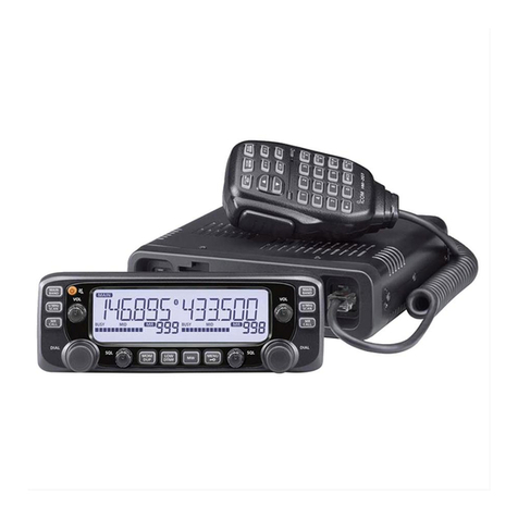
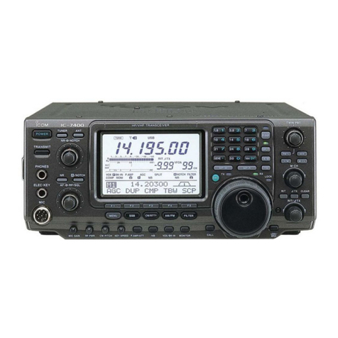
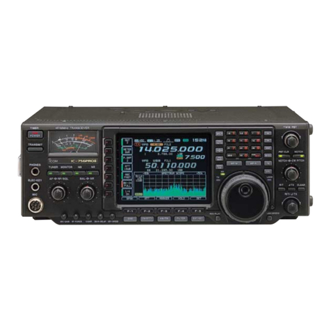
Icom ID-5100E User manual

S-15103XZ-C1
June 2014
DUAL BAND TRANSCEIVER

This service manual describes the latest technical informa-
tion for the ID-5100A and ID-5100E DUAL BAND TRANSCEIVER, at
the time of publication.
NEVER connect the transceiver to an AC outlet or to a DC
power supply that uses more than the specified voltage. This
will ruin the transceiver.
DO NOT expose the transceiver to rain, snow or liquids.
DO NOT reverse the polarities of the power supply when con-
necting the transceiver.
DO NOT apply an RF signal of more than 20 dBm (100 mW) to
the antenna connector. This could damage the transceiver’s
front-end.
To upgrade quality, any electrical or mechanical parts
and internal circuits are subject to change without notice
or obligation.
MODEL VERSION TX OUTPUT
POWER
ID-5100A
TPE 25 W
USA
50 W
KOR
EXP
ID-5100E EUR
ITR
Be sure to include the following four points when ordering
replacement parts:
1. 10-digit Icom part number
2. Component name
3. Equipment model name and unit name
4. Quantity required
<ORDER EXAMPLE>
1110003491 S.IC TA31136FNG ID-5100A MAIN UNIT 5 pieces
8820001210 Screw 2438 screw ID-5100A Top cover 10 pieces
Addresses are provided on the inside back cover for your
convenience.
ORDERING PARTS
1. Make sure that the problem is internal before dis-assem-
bling the transceiver.
2. DO NOT open the transceiver until the transceiver is dis-
connected from its power source.
3. DO NOT force any of the variable components. Turn them
slowly and smoothly.
4. DO NOT short any circuits or electronic parts. An insulated
tuning tool MUST be used for all adjustments.
5. DO NOT keep power ON for a long time when the trans-
ceiver is defective.
6. DO NOT transmit power into a Standard Signal Generator
or a Sweep Generator, otherwise the RF power may dam-
age them.
7. ALWAYS connect a 50 dB to 60 dB attenuator between the
transceiver and a Deviation Meter or Spectrum Analyzer,
when using such test equipment.
8. READ the instructions of the test equipment thoroughly
before connecting it to the transceiver.
REPAIR NOTES
INTRODUCTION CAUTION
(ID-5100A)
Icom, Icom Inc. and the Icom logo are registered trademarks of Icom Incorporated (Japan) in Japan, the United States, the
United Kingdom, Germany, France, Spain, Russia and/or other countries.

TABLE OF CONTENTS
SECTION 1 SPECIFICATIONS
SECTION 2 INSIDE VIEWS
SECTION 3 DISASSEMBLY INSTRUCTION
SECTION 4 CIRCUIT DESCRIPITON
4-1 RECEIVER CIRCUITS...................................................................................... 4-1
4-2 TRANSMITTER CIRCUITS............................................................................... 4-3
4-3 FREQUENCY SYNTHESIZER CIRCUITS ....................................................... 4-5
4-4 VOLTAGE BLOCK DIAGRAM ........................................................................... 4-6
4-5 PORT ALLOCATIONS ...................................................................................... 4-6
SECTION 5 ADJUSTMENT PROCEDURES
5-1 PREPARATION ................................................................................................. 5-1
5-2 FREQUENCY ADJUSTMENT .......................................................................... 5-2
5-3 TRANSMIT ADJUSTMENTS ............................................................................ 5-3
5-4 RECEIVE ADJUSTMENTS............................................................................... 5-5
SECTION 6 PARTS LIST
SECTION 7 MECHANICAL PARTS
SECTION 8 BOARD LAYOUTS
SECTION 9 BLOCK DIAGRAM
SECTION 10 VOLTAGE DIAGRAM

1-1
SECTION 1
.
SPECIFICATIONS
General
■
• Frequency coverage:
EUR RX 118–174 MHz*1, 375–550 MHz*2
TX 144–146 MHz, 430–440 MHz
ITR RX 118–136.99166 MHz*3, 144–146 MHz, 430–434 MHz, 435–438 MHz
TX 144–146 MHz, 430–434 MHz, 435–438 MHz
TPE RX 144–146 MHz, 430–432 MHz
TX 144–146 MHz, 430–432 MHz
USA RX 118–174 MHz*4, 375–550 MHz*5
TX 144–148 MHz, 430–450 MHz*5
KOR RX 144–146 MHz, 430–440 MHz
TX 144–146 MHz, 430–440 MHz
EXP RX 118–174 MHz*4, 375–550 MHz*2
TX 137–174 MHz*4, 400–470 MHz*2
*
1
Guaranteed only 144–146 MHz, *
2
Guaranteed only 430–440 MHz,
*3 Not guaranteed,
*
4
Guaranteed only 144–148 MHz, *
5
Guaranteed only 440–450 MHz
• Mode: F2D/F3E (FM/FM-N), F7W (DV), A3E (AM/AM-N) RX only
• Number of memory channels: 1000 channels
• Number of program scan channels: 25 channels
(2 edge frequencies in each channel)
• Number of call channels: 4 channels (2 channels × 2 bands)
• Antenna connector: SO-239
• Antenna impedance: 50 ø
• Usable temperature range: –10˚C to +60˚C; +14˚F to +140˚F
• Frequency stability: ±2.5 ppm (–10˚C to +60˚C; +14˚F to +140˚F)
•
Digital transmission speed
: 4.8 kbps
• Voice coding speed: 2.4 kbps
• Frequency resolution: 5 kHz, 6.25 kHz, 8.33 kHz, 10 kHz, 12.5 kHz, 15 kHz, 20 kHz, 25 kHz, 30 kHz, 50 kHz
(The 8.33 kHz step is selectable only when the VHF air band is selected.)
• Power supply: 13.8 V DC ±15% (negative ground)
• Current drain:
Transmit
Maximum current drain: 10.5 A (TPE version)
13.0 A (Other versions)
Receive
Standby: 1.2 A
Maximum audio: 1.8 A
• Dimensions (projections not included):
Main unit: 150(W) 40(H) 172.6(D) mm; 5.9(W) 1.6(H) 6.8(D) inch
Controller:
182.2(W) 24.8(H) 81.5(D) mm;
7.2(W) 1.0(H) 3.2(D) inch
• Weight (approximately):
Main unit: 1.3 kg; 2.9 lb
Controller: 260 g; 9.2 oz
1-2
Transmitter
■
• Modulation system:
FM/FM-N Variable reactance frequency modulation
DV GMSK reactance frequency modulation
• Maximum Deviation:
FM ±5.0 kHz
FM-N ±2.5 kHz
• Microphone impedance: 600 ø
• Spurious emission: –60 dBc
• Output power: High 25 W, Mid 15 W, Low 5 W (TPE version)
High 50 W, Mid 15 W, Low 5 W (Other versions)
Receiver
■
• Receive system: Double superheterodyne system
• IF frequencies:
Band A 1st IF 38.85 MHz
2nd IF 450 kHz
Band B 1st IF 46.35 MHz
2nd IF 450 kHz
• Sensitivity (except spurious points)
Amateur bands
FM/FM-N (12 dB SINAD)
0.18 µV
DV (BER 1%) 0.28 µV
Except Amateur bands
FM/FM-N (12 dB SINAD)
0.32 µV (137.000 to 159.995 MHz)
0.56 µV (160.000 to 174.000 MHz)
0.56 µV (375.000 to 399.995 MHz)
0.32 µV (400.000 to 499.995 MHz)
0.56 µV (500.000 to 550.000 MHz)
AM (10 dB S/N) 1 µV (118.000 to 136.99166 MHz)
• Squelch sensitivity: 0.13 µV (Threshold)
• Selectivity:
FM 60 dB
FM-N 55 dB
DV 50 dB
• Spurious and image rejection ratio:
60 dB
55 dB (A band UHF)
• AF output power: 2.0 W (at 10% distortion with an 8 øload)
• AF output impedance: 8 ø
All stated specifications are typical and subject to change without notice or obligation.

2-1
SECTION 2
.
INSIDE VIEWS
IC7
IC7
IC8
IC8
Q3
Q3
Q6
Q6
C80
IC2
IC2
IC5
IC5
IC6
IC6
X1
X1
• CONTROL UNIT
(TOP VIEW)
• CONTROL UNIT
(BOTTOM VIEW)
3.3 V REGULATOR
(IC7)
3.3 V REGULATOR
(IC6)
RESET IC
(IC5)
CPU CLOCK
(X1)
TOUCH SCREEN CONTROLLER
(IC8)
CONTROLLER CPU
(IC2)

2-2
FI104
FI104
FI105
FI105
IC1
IC1
IC3
IC3
IC4
IC4
IC100
IC100
IC101
IC101
IC102
IC102
IC103
IC103
IC104
IC104
IC107
IC107
IC108
IC108
IC109
IC109
IC110
IC110
IC111
IC111
IC112
IC112
IC113
IC113
IC117
IC117
IC120
IC120
IC121
IC121
IC122
IC122
IC123
IC123
IC124
IC124
IC125
IC125
IC202
IC202
IC203
IC203
IC205
IC205
IC207
IC207
IC208
IC208
IC301
IC301
IC302
IC302
IC307
IC307
IC308
IC308
IC312
IC312
IC314
IC314
IC315
IC315
IC316
IC316
IC317
IC317
IC318
IC318
IC319
IC319
IC320
IC320
IC323
IC323
IC324
IC324
IC400
IC400
IC403
IC403
IC404
IC404
IC405
IC405
IC406
IC406
IC407
IC407
X301
X301
X400
X400
LO AMP & LO SW
(Band B)
• MAIN UNIT
(TOP VIEW)
DSP
(IC400)
VOLTAGE DETECTOR
(IC324)
AF SW
(IC205)
IF IC (Band A)
(IC121)
AF SW
(IC100)
AF SW
(IC104) AUDIO SIGNAL PROCESSOR
(IC103)
EXPANDER
(IC316)
AF SW
(IC109)
5 V REGULATOR
(IC319)
ELECTRIC VOLUME IC
(IC110)
AF LPF & HPF
(IC407)
EEPROM
(IC301)
RTC BACKUP BATTERY
(IC301)
REAL TIME CLOCK (RTC) IC
(IC302)
RS232 LEVEL CONVERTER
(IC318)
AF SW
(IC111)
AF BUFFER
(IC117)
AF SW
(IC113)
AF LPF & HPF
(IC406)
DSP CLOCK
(X400)
D/A CONVERTER
(IC1)
EXPANDER
(IC317)
1ST MIXER
(Band A)
EXPANDER
(IC315)
IF IC (Band B)
(IC120)
1ST IF FILTER (Band B)
(FI104)
1ST IF FILTER (Band A)
(FI105)
VCO
(Band B)
VCO
(Band A)
1ST MIXER
(Band B)
LO AMP & LO SW
(Band A)

2-3
• MAIN UNIT
(BOTTOM VIEW)
2ND IF FILTER (Band A)
(FI100)
MAIN CPU CLOCK
(X300)
DSP FLASH ROM
(IC401)
SUB CPU CLOCK
(X302)
AF POWER AMP
(IC106)
AF POWER AMP
(IC105)
6 V SWITCHING REGULATOR
(IC309)
PLL IC (Band B)
(IC206)
AF SW
(IC119)
REFERENCE FREQUENCY
OSCILLATOR (Band B)
(X201)
APC AMP
(IC2)
DISCRIMINATOR (Band A)
(X101)
2ND IF FILTER (Band A)
(FI101)
SRAM
(IC304)
8 V REGULATOR
(IC321)
8 V REGULATOR
(IC313)
MAIN CPU
(IC300)
3.3 V REGULATOR
(IC311)
LINER CODEC
(IC402)
SUB CPU
(IC303)
3.3 V REGULATOR
(IC306)
3.3 V REGULATOR
(IC305)
QUAD BUS BUFFER
(IC200)
PLL IC (Band A)
(IC201)
REFERENCE FREQUENCY OSCILLATOR (Band A)
(X200)
2ND IF FILTER (Band A)
(FI102) 2ND IF FILTER (Band A)
(FI103)
DISCRIMINATOR (Band A)
(X102)
CURRENT DETECTOR
(IC310)

3-1
SECTION 3
.
DISASSEMBLY INSTRUCTION
M
Removing the CONTROL UNIT from the controller.
1) Remove two dials and four knobs from the front
panel.
2) Remove four screws from the rear panel.
BE CAREFUL when you disassemble the rear panel from
the CONTROL UNIT. Otherwise the flat cable and the
connector may be cut.
Knob
Knob
Dial
Dial
Flat cable
Four screws
Flat cable
Rear panel
CONTROL UNIT
Flat cable
flat cable
Release the locks
Pull straight
FLAT CABLE
Flat cable
Flat cable
BE CAREFUL about the locks.
Four screws
CONTROL UNIT
FRONT PANEL
Flat cable
flat cable
Release the locks
Pull straight
FLAT CABLE
Flat cable
Flat cable
BE CAREFUL about the locks.
3) Take off the rear panel carefully in the direction of
the arrow, and then disconnect the flat cable.
4) Disconnect two flat cables.
5) Remove four screws from the CONTROL UNIT.
6) Remove the CONTROL UNIT from the front panel.
(Continued on the right above.)

3-2
1) Remove eight screws from the top cover.
2) Remove the clip and disconnect the speaker cable.
3) Remove eight screws from the bottom cover.
Bottom cover
Eight screws
Flat cable
Speaker
Clip
Flat cable
SPEAKER
CABLE
Bottom cover
Eight screws
Flat cable
14 screws
Flat cable
Flat cable
FAN
CABLE
UNSOLDER
Solder
remover
Flat cable
MAIN UNIT
4) Remove total of 14 screws from the MAIN UNIT.
5) Disconnect the cooling fan cable, and unsolder five
points (at the antenna connector and the DC cable).
6) Remove the MAIN UNIT from the chassis in the di-
rection of the arrow.
(Continued on the right above.)
Before disassembling:
REMOVE the SD card if inserted. Otherwise the MAIN
UNIT and chassis cannot be separated.
M Removing the MAIN UNIT from the chassis.

4-1
SECTION 4
.
CIRCUIT DESCRIPTION
4-1 RECEIVE CIRCUITS
RF CIRCUITS (MAIN UNIT)
VHF BAND (108–174 MHz)
The RF signal from the antenna is passed through two LPFs
(L90, L94, L96, C409, C418 and L79, L83, L87, C378, C386,
C394), ANT SW (D66, D69, D70 and D77), and then applied
to the RF AMP (Q24).
• Band A
The amplified signal is passed through the ATT (D34), BPF
(D28, D88, L24, L26, L31 L34, C127 and C128), and then
applied to another RF AMP (Q20).
The amplified signal is applied to the 1st IF circuit, through
the BPF (D20, D87, L10, L18, C71 and C74) and RX circuit
SW (D14).
• Band B
The amplified signal is passed through the ATT (D33), BPF
(D27, D85, L23, L25, L32, L33, C125 and C126), and then
applied to another RF AMP (Q19).
The amplified signal is applied to the 1st IF circuit, through
the BPF (D19, D86, L9, L17, C69 and C70) and RX circuit
SW (D13).
UHF BAND (380–479 MHz)
The RF signal from the antenna is passed through the LPF
(L90, L94, L96, C409 and C418) and HPF (L84, L88, C391,
C395 and C402) and ANT SW (D68, D73, D75 and D84), and
then applied to the RF AMP (Q23).
• Band A
The amplified signal is passed through the ATT (D32), BPF
(D24, D26, L21, L28, C113 and C114), and then applied to
the RF AMP (Q18).
The amplified signal is applied to the 1st IF circuit, through
the BPF (D12, D16, L4, L12, C42 and C43) and RX circuit
SW (D8).
• Band B
The amplified signal is passed through the ATT (D31), BPF
(D23, D25, L22, L27, C107, C111, C112 and C121), and then
applied to the RF AMP (Q17).
The amplified signal is applied to the 1st IF circuit, through
the BPF (D11, D15, L3, L11, C36, C40, C41 and C49) and
RX circuit SW (D7).
BPF
HPF
RF
AMP
RF
AMP
ATT
TX/RX
SW
BPF
BPF
BPF
ATT
RF
AMP
LPF
BPF
ANTENNA
BPF
RF
AMP BPF
LPF
RF
AMP
RF
AMP
ATT
TX/RX
SW
BPF
ATT
RX
SW
RX
SW
RX
SW
RX
SW
LIMITER LIMITER
118-550MHz
118-174MHz
375-550MHz
118-174MHz
VHF BAND
UHF BAND
375-550MHz
Band A
Band A
Band B
Band B
400-470MHz
137-174MHz
1st IF
circuit
1st IF
circuit
D68/D73/D75
D66/D69/
D70/D77
D79D81
Q24
D34D28/D88Q20D20/D87D14
D33D27/D85Q19D19/D86D13
Q23
D32
D22/D24/
D26/D30
Q18
D10/D12/
D16/D18
D8
D31
D21/D23/
D25/D29
Q17
D9/D11/
D15/D17
D7
D84
• RF CIRCUITS

4-2
1ST IF CIRCUITS (MAIN UNIT)
• Band A
The RX signal from the RF circuit is applied to the 1st mixer
(IC125) and mixed with the 1st LO signal, resulting in the
38.85 MHz 1st IF signal. The converted signal is passed
through the 1st IF filter (FI105), and then applied to the 1st
IF AMP (Q138). The amplified signal is applied to the 2nd IF
circuit, through the limiter (D114).
2ND IF CIRCUITS (MAIN UNIT)
• Band A
The 1st IF signal from the 1st IF circuit is applied to the IF IC
(IC121, pin 20), which contains the 2nd IF AMP, 2nd mixer,
FM demodulator, and so on.
The 1st IF signal is mixed with the 38.4 MHz 2nd LO signal,
resulting in the 450 kHz 2nd IF signal. The converted signal
is passed through the external 2nd IF filter (FM mode: FI103,
FM-N or DV mode: FI102) to remove sideband noise.
While operating in the FM or AM mode, the filtered signal is
amplified by the 2nd IF AMP, and then demodulated by the
internal demodulator circuit. The demodulated signal is ap-
plied to the RX AF circuit, through the RX mode SW (IC119),
AF filter (Q113 and Q140) and AF SW (IC111).
While operating in the DV mode, the filtered signal is ampli-
fied by the 2nd IF AMP, and then demodulated by the inter-
nal demodulator circuit. The demodulated signal is applied
to the digital demodulation circuit, through the RX mode SW
(IC119) and buffer AMP (IC117).
IF
AMP BPF
XTAL RIF
1st LO
Band B
46.35MHz
Q137/
D115/D117
FI104
2nd IF
circuit
IC124
LIMITER
D113
IF
AMP BPF
XTAL LIF
1st LO
Band A
38.85MHz
Q138/
D116/D118
2nd IF
circuit
FI105
IC125
LIMITER
D114
BUFF
BPF
CERAMIC BPF
CERAMIC
X3
DET OUT
SELECT
AF
DIGI/AN
AFMUTE FIL
IF IC
FM
FM/AM
DV
Digital
demodulation
Cricut
RX AF
Cricut
AM
Band A
38.4MHz
SELECTOR
WIDE/NARROW
12.8MHz
X200
Q200
IC111 Q113/Q140
IC117 IC119 IC121
Q122/Q124/Q142
Q128/D107/D108
D111/D112
FI102 FI103
X102
BPF
CERAMIC
BPF
CERAMIC
BUFF
X3
DET OUT
AFMUTE FIL
IF IC
AF WIDE/NARROW
DIGI/AN
SELECT
SELECTOR
15.3MHz
AM
FM
FM/AM
DV
Digital
demodulation
Cricut
RX AF
Cricut
Band B
45.9MHz X201
Q220
IC111 Q112/Q139
IC117 IC120IC119
Q121/Q123/Q141
Q127/D105/D106
D109/D110
FI100 FI101
X101
• 1ST IF CIRCUITS (Band B)
• 1ST IF CIRCUITS (Band A)
• 2ND IF CIRCUITS (Band A)
• 2ND IF CIRCUITS (Band B)
• Band B
The 1st IF signal from the 1st IF circuit is applied to the IF IC
(IC120, pin 20), which contains the 2nd IF AMP, 2nd mixer,
FM demodulator, and so on.
The 1st IF signal is mixed with the 45.9 MHz 2nd LO signal,
resulting in the 450 kHz 2nd IF signal. The converted signal
is passed through the external 2nd IF filter (FM mode: FI101,
FM-N or DV mode: FI100) to remove sideband noise.
While operating in the FM or AM mode, the filtered signal is
amplified by the 2nd IF AMP, and then demodulated by the
internal demodulator circuit. The demodulated signal is ap-
plied to the RX AF circuit, through the RX mode SW (IC119),
AF filter (Q112 and Q139) and AF SW (IC111).
While operating in the DV mode, the filtered signal is ampli-
fied by the 2nd IF AMP, and then demodulated by the inter-
nal demodulator circuit. The demodulated signal is applied
to the digital demodulation circuit, through the RX mode SW
(IC119) and buffer AMP (IC117).
• Band B
The RX signal from the RF circuit is applied to the 1st mixer
(IC124) and mixed with the 1st LO signal, resulting in the
46.35 MHz 1st IF signal. The converted signal is passed
through the 1st IF filter (FI104), and then applied to the 1st
IF AMP (Q137). The amplified signal is applied to the 2nd IF
circuit, through the limiter (D113).

4-3
DIGITAL DEMODULATION CIRCUIT (MAIN UNIT)
While operating in the DV mode, the demodulated signal (dig-
ital audio signal) is passed through the LPF (Band A: R1195,
R1206, C1461 and C1475/Band B: R1194, R1205, C1460
and C1474) and amplified by the AF AMP (Band A: IC407/
Band B: IC406). The amplified signal is applied to the liner
codec (IC402) to be converted into the digital audio signal.
The digital audio signal is demodulated by the DSP (IC400),
and then applied to the linear codec (IC402) again, to be de-
coded into an analog audio signal.
The decoded AF signal is applied to the RX AF circuit, through
the HPF (Band A: IC407/Band B: IC406) and LPF (Band A:
IC407/Band B: IC406) and AF SW (IC111).
4-2 TRANSMIT CIRCUITS
TX AF CIRCUIT (MAIN UNIT)
The AF signal from the microphone (MIC signal) is passed
through the MIC SW (IC100) and ATT (IC100), and then ap-
plied to the MIC AMP (IC102).
The amplified signal is applied to the audio processor LSI
(IC103), through the mute SW (IC104).
The audio processor LSI contains 16-bit liner CODEC, MIC
AMP, audio filters, D/A converter, and so on.
• When operating in the DV mode
The applied signal is further amplified by the ALC AMP. The
amplified signal is applied to the liner CODEC, to be encoded
into a digital audio signal.
The digital audio signal is processed by the DSP (IC400), and
then passed through the mode SW (IC104) and LPF (IC103),
and then applied to the D/A converter (IC103), to be adjusted
in level.
• When operating in the FM/FM-N mode
The applied signal is passed through the HPF (IC103), IDC
(IC103), LPF (IC103), mode SW (IC104) and LPF (IC103),
and then applied to the D/A converter (IC103) to be adjusted
in level.
The level-adjusted signal is applied to the modulation circuit.
LPF
LPF
HPF
HPF
AMP LPF
AMP LPF R_DDET
L_DDET
CODEC
LINEAR
DSP
IC400
IC402
DIGI/AN
AFMUTE
IC111
AFMUTE
DIGI/AN
IC111
L_DAF
R_DAF
IC407 IC407
IC406 IC406
L_DAF
R_DAF
IC407
IC406
AF
AMP
SP1
AF
AMP
J102
J101
[SP2]
[SP1]
AFSW
SP
MUTE
VR
ELEC.
MUTE
SP
SP
MUTE
A band AF
B band AF
IC106 Q106
IC105 Q104 Q105
IC109 IC110
RX AF CIRCUIT (MAIN UNIT)
The demodulated AF signal from the AF SW (IC111) is ap-
plied to the electric volume (IC110), which separately adjusts
the A and B bands AF signal in level. The level-adjusted AF
signal is passed through the AF line SW (IC109).
When the AF signal is output from the internal speaker
or [SP1] jack:
The AF signal is passed through two speaker mute SWs
(Q105 and Q104), and then amplified by the AF power AMP
(IC105).
The amplified AF signal is output to the internal speaker
(CHASSIS: SP1) or external speaker, through the [SP1] jack
(J101).
When the AF signal is output from the [SP2] jack:
The AF signal is passed through the speaker mute SW
(Q106), and then amplified by the AF power AMP (IC106).
The amplified AF signal is applied to the [SP2] jack (J102).
D/A
LPF
HPF
J100
1
2
3
4
5
6
7
8
ALC
AMP
LPF
IDC
D/AA/D
MIC
AMP
BUFF
ATT MUTE
SW
MIC
FMFM
DV
DV
BTMIC
SW
Audio Processor LSI
BTMIC
SELECT
MODE
DSP
IC307
IC100 IC100 IC102
IC103
IC104
IC104
IC400
IC103 IC103
• DIGITAL DEMODULATION CIRCUIT
• RX AF CIRCUITS
• TX AF CIRCUIT

4-4
MODULATION CIRCUITS (MAIN UNIT)
The MIC signal from the TX AF circuits is applied to the VCO
as the GMSK (For the DV mode) or Frequency Modulation
(For the FM mode) modulation signal.
VHF BAND
The modulation signal is applied to the VHF VCO (Q211,
D203, D204 and D228).
The modulated VCO output signal is amplified by the buffer
(Q215) and LO AMP (IC203), and then applied to the TX AMP
circuits as the TX signal, through the LO SW (D50).
UHF BAND
The modulation signal is applied to the UHF VCO (Q232,
D223, D224 and D227) as a modulation signal.
The modulated VCO output signal is amplified by the buffer
(Q235) and LO AMP (IC208), and then applied to the TX AMP
circuits as the TX signal, through the LO SW (D52).
TX AMP CIRCUITS (MAIN UNIT)
VHF BAND
The TX signal is passed through the LPF (L50, L51, C215,
C220 and C225) and ATT (R146, R147 and R151), and then
sequentially amplified by the YGR (Q36), drive AMP (Q40)
and power AMP (IC3).
The amplified TX signal is passed through the LPF (L67,
C291 and C297), TX output power detector (D59 and D63),
ANT SW (D66) and two LPFs (L90, L94, L96, C409, C418
and L79, L83, L87, C378, C386, C394), before being applied
to the antenna.
UHF BAND
The TX signal is passed through the HPF (L52 and C232) and
ATT (R155, R156 and R162), and then sequentially amplified
by the YGR (Q38), drive AMP (Q41) and power AMP (IC4).
The amplified TX signal is passed through the LPF (L69,
C310 and C319), TX output power detector (D62 and D67),
ANT SW (D68 and D84), HPF (L84, L88, C391, C395 and
C402) and LPF (L90, L94, L96, C409, C418), before being
applied to the antenna.
APC CIRCUITS (MAIN UNIT)
At the TX output power detector, the RF signal at the LPFs
(VHF band: L68, C301, C302 and C326/UHF band: L73,
C322, C323 and C350) is rectified by the diodes (VHF band:
D59 and D63, UHF band: D62 and D67), and it is used as the
TX power sensing voltage.
The voltage is applied to the APC AMP (IC2), and the output
voltage controls the bias voltages of the power AMP (VHF
band: IC3, UHF band: IC4) to keep the TX output power con-
stant.
HPFLPF
PWR
AMP TX/RX
SW
LPF
TX/RX
SW
AMP
LO
AMP
LO DRIVE
AMP
PWR
AMP
LPF
ANTENNA
BUFF YGR
ATT
LPF
DRIVE
AMP
HPF
TX/RX
SW
BUFF YGR
ATT
APC
CTRL
PWR
DET
PWR
DET
LPF
TX/RX
SW
LPFHPF
118-550MHz
118-174MHz
375-550MHz
VCOMOD MOD
MUTE
UHF band
VHF band
UHF TX VCO
VHF TX VCO
IC205
Q215
Q211
Q207 IC203
Q232
Q227 Q235 IC208 D52
D50
Q38 Q41 IC4 D62/D67 D68/D73/D75
Q36 Q40 IC3 D59/D63
D66/D69/
D70/D77
UHF RX circuit
VHF RX circuit
IC2
D84
• TX AMP AND APC CIRCUITS

4-5
4-3 FREQUENCY SYNTHESIZER CIRCUIT
(MAIN UNIT)
VCOs
The ID-5100A/E has total of five VCOs: three VCOs for Band
A and another two for Band B.
• Band A
VHF VCO #1
(Used when the Heterodyne function is set to "Normal")
The VHF VCO #1 (Q211, D204, D206 and D228) generates
both 1st LO signal (for receiving a VHF signal on Band A)
and the VHF TX signal. The output of buffer (Q215) is ampli-
fied by the LO AMP (IC203), and then used as the VHF TX/
RX LO signal.
While receiving, the LO signal is applied to the 1st IF mixer
(IC125) for receiving a signal on the VHF band, through the
RX LO SW (D212 and D217) and LPF (L314, L316, C986,
C992 and C997).
While transmitting, the LO signal is applied to the TX AMP
circuits, through the LO SW (D50).
VHF VCO #2
(Used when the Heterodyne function is set to "Reverse")
The VHF VCO #2 (Q237, D238 and D239) generates the 1st
LO signal (for receiving a VHF signal on Band A). The output
of buffer (Q215) is amplified by the LO AMP (IC203), and
then applied to the 1st IF mixer (IC125) for receiving a signal
on the VHF band, through the RX LO SW (D212 and D217)
and LPF (L314, L316, C986, C992 and C997).
UHF VCO
The UHF VCO (Q205, Q210, D201, D202 and D205) gener-
ates the 1st LO signal (for receiving a UHF signal on Band
A). The output of buffer (Q214) is amplified by the LO AMP
(IC203), and then applied to the 1st IF mixer (IC125), through
the RX LO SW (D213 and D216) and LPF (L315, C988 and
C995).
• Band B
VHF VCO
The VHF VCO (Q228, Q233, D225, D226 and D230) gener-
ates the 1st LO signal (for receiving a UHF signal on Band
A). The output of buffer (Q236) is amplified by the LO AMP
(IC208), and then applied to the 1st IF mixer (IC124), through
the RX LO SW (D235 and D237) and LPF (L338, L339,
C1103, C1105 and C1106).
UHF VCO
The UHF VCO (Q232, Q227, D223, D224, D227 and D229)
generates both 1st LO signal (for receiving a UHF signal on
Band B) and the UHF TX signal. The output of buffer (Q235)
is amplified by the LO AMP (IC208), and then used as the
UHF TX/RX LO signal.
While receiving, the LO signal is applied to the 1st IF mixer
(IC124) for receiving a signal on the UHF band, through the
RX LO SW (D234 and D236) and LPF (L337, C1102 and
C1104).
While transmitting, the LO signal is applied to the TX AMP
circuits, through the LO SW (D52).
PLL
•Band A
A portion of VHF and UHF VCOs output signal is amplified by
the buffer (Q213), and then fed back to the PLL IC (IC201).
The PLL IC (IC201) phase-compares the output of reference
frequency oscillator (TCXO: X200) and VCO, and the phase
difference is output as the charge pump current. The current
is passed though the loop filter (R715, R717, R719, R722,
C924, C926 to C928 and C930) to be converted into the lock
voltage, which controls the oscillating frequency of VCO.
When the oscillation frequency drifts, its phase changes from
that of the reference frequency, causing a lock voltage change
to compensate for the drift in the VCO oscillating frequency.
• Band B
A portion of VHF and UHF VCOs output signal is amplified by
the buffer (Q234), and then fed back to the PLL IC (IC206).
The PLL IC (IC206) phase-compares the output of reference
frequency oscillator (TCXO: X201) and VCO, and the phase
difference is output as the charge pump current. The current
is passed though the loop filter (R797, R799, R802, R805,
C1041, C1043 to C1045 and C1048) to be converted into the
lock voltage, which controls the oscillating frequency of VCO.
When the oscillation frequency drifts, its phase changes from
that of the reference frequency, causing a lock voltage change
to compensate for the drift in the VCO oscillating frequency.
TX/RX
SW
AMP
AMP
FIL
LOOP
BUFF
BUFF
BUFF
BUFF
BUFF
BUFF
PLL
IC
LPFLPF
X3
TX/RX
SW
X3
FIL
LOOP
PLL
IC
RX
SW
IF IC
IF IC
15.3 MHz
38.4 MHz
45.9 MHz
12.8 MHz
R_UHF
R_VHF
L_UHF
L_VHF
IC207/Q222
X201
IC206
Q220
IC202/Q202
X200
IC201
Q200 Q213
Q215
Q211
Q210 Q214 IC203
Q234
Q236
Q233
Q232
Q235
IC208 D52/D234/D235
D50
D212/D213
D236
D237
D216
D217
2nd LO
1st LO
1st LO
2nd LO
IC121 A band
B band
IC120
IC125
1st mixer
1st mixer
IC124
LPFLPF
RX
SW
D223,D224,
D227,D227
D225,D226,D230
D201,D202,D205
D203,D204,
D206,D228
Q237
D238,D239
TX:400-470 MHz
RX:353.65-516.35 MHz
RX:164.35-220.35 MHz
RX:361.15-511.15 MHz
137-174 MHz
RX:79.15-135.15 MHz
TX:
RX:
156.85-212.85 MHz
• FREQUENCY SYNTHESIZER CIRCUIT

4-6
W300
+8
REG
PWR
CTRL
UT8
VCC
SW
CPU3.3V
5V
PCON
REG
REG
3VS
5VS
FANHV
REG
IDET
DETECT
CURRENT
NOISE
FILTER
REG
VT8
REG
3.3V
UTX_C
VTX_C
I SENS
3.3V
CTRL8V
REG
8V
BT3.3V
BT3V
REG
UT8
VT8
HV
CONT8V
SW
REG(6V)
PSC
SW
SD3V
REG SD3.3V
LOW V
DET
PDV ALARM
To BT
To CPU
REG
4.2V CAP
SUPER
MAIN UNIT
IC310
Q302/Q306 IC313
Q301
IC309
IC320
IC305
IC306
IC311
IC323 C1340 IC314
IC319Q303
IC321
Q32/Q34
Q27/Q28
IC403
3.3V
REG
IC404
1.3V
REG
DSP3.3V
DSP1.3V
VCC
IC324
Ball
No. Line Name Description I/O
7 TWDTX Touch panel controller touch sens-
ing data. O
14 RESET Reset signal input. I
15 R_VOLV Band B [VOL] input. I
16 R_SQLV Band B [SQL] input. I
17 L_VOLV Band A [VOL] input. I
18 L_SQLV Band A [SQL] input. I
25 G_TXD GPS data. O
26 G_RXD I
29 DIM_DA LCD backlit brightness control. O
30 G_RES GPS module (EP13) reset.
L=Resets. O
31 GPSC
GPS module (EP13) power supply
control.
L=GPS module is activated.
O
32 LCDRST LCD controller reset.
L=Resets. O
33 TEMP LCD controller temperature sens-
ing voltage. I
38–
41
LCDD4–
LCDD7 LCD control data. I/O
47 FLTXD Control signal to the main CPU
(IC300). O
48 FLRXD Control signal from the main CPU
(IC300). I
51 L_DIALB Band A [DIAL] phase-B. I
52 L_DIALA Band A [DIAL] phase-A. I
53 R_DIALB Band B [DIAL] phase-B. I
54 R_DIALA Band B [DIAL] phase-A. I
58 LCDCD
LCD controller data/command se-
lect.
H=While sending the control data.
O
61 LCDD0 LCD control data. I/O
62 LCDD1
65 TWCS Touch panel controller chip select.
L=While inputting/outputting data. O
66 TWBUSY Touch panel controller status.
H=Busy. I
78 TWPIRQ Touch panel controller interrupt.
L=Touching detected. I
79 TWDCLC Touch panel controller serial
clock. O
80 TWDRX Touch panel controller serial data. O
81 LCDD2 LCD control data. O
86 LCDWR0 Touch panel controller read/write
control. O
88 LCDCS LCD controller chip select. O
• CONTROLLER CPU (CONTROL UNIT: IC2)
4-5 PORT ALLOCATIONS4-4 VOLTAGE DIAGRAM

4-7
Ball
No. Line Name Description I/O
A4 R_LV Lock voltage input. (Band B) I
A6 VIN External power supply voltage. I
A7 L_WXALT WX alert signal (1050 Hz). (Band
A) I
A8 MICUD The [UP]/[DOWN] key input from
the microphone. I
A9 AUDI Response signal from the audio
IC. I
A11 PSC 5VS power supply line control.
L=While in the power save mode. O
A12 DA_STB D/A converter serial strobe. O
B1 DTMF DTMF tone, European tone and
beep sound signals. O
B4 R_RSSI RSSI voltage. (Band B) I
B7 IDET Transmit current sensing voltage. I
B8 TEMP Transceiver temperature sensing
voltage. I
B9 AURES Audio IC reset.
L=Reset. O
C2 DTCS
TSQL/DTCS tone filter switching
control.
H=While the DTCS tone is used.
O
C4 R_DTCSIN TSQL/DTCS tone signal. (Band
B) I
C7 L_DTCSIN TSQL/DTCS tone signal. (Band
A) I
C9 DTMUTE
Tone signal (BEEP/DTMF/
ETONE) modulation mute.
L=Mute.
O
C11 DSP_PD DSP power down control.
H=Power down. O
D1 DA_DATA Serial data to the D/A converter. O
D2 BTRXD Serial data from the Bluetooth®
unit. I
D4 R_WXALT Weather alert signal (1050 Hz)
detect. (Band B) I
D5 R_LV Lock voltage. (Band B) I
D6 VOX VOX sensing voltage. I
D7 L_RSSI RSSI voltage. (Band A) I
D8 AUSTB Audio IC serial strobe. O
D11 DA_CK Serial clock to the D/A converter. O
E4 BTTXD Serial data to the Bluetooth®unit. O
G1 RESET CPU reset signal.
L=Reset. I
G3 BT_RES Bluetooth®unit reset signal.
H=Reset. O
G4 MIC_PTT PTT input from the microphone. I
H14 SCSCK Serial clock to the sub CPU
(IC303). O
H15 SCRXD Serial data from the sub CPU
(IC303). I
J4 RTC_IRQ
Interrupt detection from the real
time clock IC.
L=Alerm detected.
I
J12 BWD
The [RWD] key input from the Blu-
etooth®unit.
L=When pushed.
I
J13 BTPLAY
The [PLAY] key input from the Blu-
etooth®unit.
L=When pushed.
I
Ball
No. Line Name Description I/O
J15 BT_SW
Bluetooth®unit power supply con-
trol.
H=The Bluetooth®unit is acti-
vated.
O
K1 L_SQL Noise level detection. (Band A)
H=Noise signal is detected. I
K3 IOSTB Expander serial strobe. O
K14 FWD
The [FWD] key input from the Blu-
etooth®unit.
L=When pushed.
I
K15 IOEN Expander chip enable. O
M1 98_DATA Control serial data from the micro-
phone. I
M2 TX_DATA Control serial data to the CPU on
the CONTROL UNIT. O
M5 DSP_STB DSP serial strobe. O
M7 ECK EEPROM serial clock. O
M8 L_UNLK PLL unlock detection. (Band A)
L=Unlocked. I
M9 VOL_DATA Serial data to the audio volume
IC. O
M12 TX232 UART data (RS-232C).
(4800/9600/38400 bps) O
N1 RX_DATA Control serial data from the CPU
on the CONTROL UNIT. I
N2 SD_SENC SD card insert detection.
L=Inserted. I
N3 SD_TXD Serial data to the SD card. O
N4 DSP_SI DSP serial data. I
N5 CLIN CI-V/CLONE UART data.
(300–38400 bps) I
N6 RTC_SDA Serial data to/from the real time
clock IC. I/O
N7 ESIO EEPROM serial data. I/O
N9 VOL_CK Serial clock to the audio volume
IC. O
N12 DATA Common serial clock to the D/A
converter and expander. O
N13 SCTXD Serial data to the sub CPU
(IC303). O
P1 SD_CS Chip select to the SD card. O
P2 SD_SCK Serial clock to the SD card. O
R8 R_UNLK PLL unlock detection. (Band B)
L=Unlocked. I
K4 DSP_REQ DSP "REQEST" signal. I
P4 DSP_CK DSP serial clock. O
P5 PDV Power supply voltage drop detect. I
P6 H_PTT
[PTT] input from the Bluetooth®
unit.
L=Pushed.
I
P7 SD_SW
SD card driver power supply con-
trol.
H=SD card driver is activated.
O
P10 SCACK "ACK" signal from the sub CPU. I
P12 BTUNIT Bluetooth®unit mount detect.
L=Mounted. I
P13 RX232 RS-232C UART data.
(4800/9600 bps) I
R1 SD_RXD Serial data from the SD card. I
R2 DSP_SO DSP serial data. O
• MAIN CPU (MAIN UNIT: IC300)

4-8
Ball
No. Line Name Description I/O
R4 CLOUT CI-V/CLONE UART data.
(300–38400 bps) O
R5
DSP_RESET
DSP reset control.
L=Reset. O
R6 RTC_SCL Serial clock to the real time clock
IC. O
R7 PCON Main power supply line control.
H=Power ON. O
R9 SD_PTC SD card write protect control.
H=Write protect. O
R10 SCRES Sub CPU reset. O
R11 SCTRG "TRG" signal to the sub CPU. O
R12 SCTXS "TXS" signal to the sub CPU. O
R13 CK Common serial clock to the D/A
converter and expander. O
R14 MICSEL External microphone connection
detect. I
59 L_AFMUTE AF output mute. (A band)
H=Mute. O
56 MICMUTE MIC mute switch control.
H=Mute. O
27 DCSFT DSP clock shift control.
L=+600 Hz shifted. O
17 R_PLLSTB PLL serial strobe. (Band B) O
63 R_AFMUTE RX AF mute control. (Band B)
L=Mute. O
55 PLAY
Modulation signal line switching
control.
H=Recorded audio is transmitted.
O
22 VTX_C
VHF band transmit circuit power
control.
H=While transmitting.
O
23 UTX_C
UHF band transmit circuit power
control.
H=While transmitting.
O
20 L_PLLSTB PLL serial strobe. (Band A) O
*: Clock frequency shifting range.
Line name CLSFT1 CLSFT2 Shifting range
Line state
H H –1.2 kHz
H L ±0 kHz
L L +1.2 kHz
Ball
No. Line Name Description I/O
1 L_REFC Reference frequency control.
(Band A) O
2 R_REFC Reference frequency control.
(Band B) O
7 SCRES Sub CPU reset. I
18 PLLCK PLL serial clock. O
19 PLLDATA PLL serial data. O
31 AF_SW
AF output control.
H=AF signal is output from the ex-
ternal speaker.
O
24 L_RMUTE AF mute control. (Band A)
L=Mute. O
25 R_RMUTE AF mute control. (Band B)
L=Mute. O
26 DTCS_SEL
Tone signal (CTCSS/DTCS) filter
switching control.
H=While sending DTCS signal.
O
34
MAIN_DASEL
Operating mode (FM/DV) switch-
ing control.
H=While operating in the DV
mode.
O
36 MIC1 Microphone gain control. O
48 SCSCK Sub CPU clock. I
49 SCTXD Sub CPU data to the main CPU. I
50 SCRXD Main CPU data. O
51 MIC2 Microphone gain control. O
52 SCTRG "TRG" signal from the main CPU. I
53 SCTXS "TXS" signal from the main CPU. I
57 VRX_RPT
Demodulated signal polarity
switching control.
H=While operating on the VHF
band.
O
58 URX_RPT
Demodulated signal polarity
switching control.
H=While operating on the UHF
band.
O
60 CLSFT3
Sub CPU clock frequency shift
control.
H=Shifted.
O
61 CLSFT2* Main CPU clock frequency shift
control. O
62 CLSFT1*
64 SCACK Sub CPU "ACK" signal to the main
CPU. O
• SUB CPU (MAIN UNIT: IC303)
• MAIN CPU (MAIN UNIT: IC300) (continued)

5-1
SECTION 5
.
ADJUSTMENT PROCEDURE
MCONNECTION
5-1 PREPARATION
MREQUIRED TEST EQUIPMENT
EQUIPMENT GRADE AND RANGE EQUIPMENT GRADE AND RANGE
DC power supply Output voltage: 13.8 V DC
Current capacity: More than 20 A
JIG cable Modified 8-pin modular jack
(See the illustration shown below.)
Audio generator Frequency range: 300–3000 Hz
Output level: 1–500 mV
RF power meter
(terminated type)
Measuring range: 1–100 W
Frequency range: 100–600 MHz
Impedance: 50
SWR: Less than 1.2 : 1
Standard signal
generator (SSG)
Frequency range: 0.1–600 MHz
Output level: –20 to +90 dBµ
(–127 to –17 dBm)
Frequency counter
Frequency range: 0.1–600 MHz
Frequency accuracy: ±1 ppm or better
Sensitivity: 100 mV or better
AC millivoltmeter Measuring range: 10 mV to 10 V
Terminator Impedance: 50
Capacity: More than 100 W
Modulation
Analyzer
Frequency range: 30–600 MHz
Measuring range: DC to ±10 kHz Attenuator Power attenuation: 50 dB
Capacity: More than 100 W
MJIG CABLE
8-pin modular jack
q
iuytrew
q
w
e
r
t
y
u
i
8V
MICU/D
EXTMIC
PTT
MICE
MIC
GND
MICIN
y(MIC)
w(MICU/D)
u(GND)
r(PTT)
u(GND)
t(MICE)
AUDIO GENERATOR
(300–3000 Hz/1–500 mV)
+−
22 kΩ
[PTT]
+−
AC MILLIVOLT METER
(10 mV to 10 V)
JIG cable
To the MICROPHONE CONNECTOR
ID-5100A/E (Rear view)
FM
deviation meter
to the antenna connector
Attenuator
40 dB
RF power meter
0.1–100 W/50 Ω
Frequency
counter
Standard signal generator
–20 to 90 dBµ
(–127 dBm to –17 dBm)
DO NOT transmit while
an SSG is connected to
the antenna connector.
CAUTION!:
SAVE the originally programmed contents (Memory channel contents, set mode settings, and so on.), before starting
adjustment. When all adjustments are completed, these contents in the transceiver may be cleared.

5-2
ADJUSTMENT ITEM ADJUSTMENT CONDITIONS OPERATION VALUE
REFERENCE
FREQUENCY
(Band A)
[REF] 1 • Connect an RF power meter to the antenna
connector.
• Loosely couple a Frequency Counter to the
antenna connector.
• Transmitting
Rotate Band B [DIAL] to adjust
the transmit frequency, and then
touch [ENT] during transmit.
Displayed
frequency
(±200 Hz)
(Band B) 2
MENTERING THE ADJUSTMENT MODE
1) Connect the JIG cable to the MICROPHONE CONNECTOR (see the illustration on page 5-1).
2) Turn Band A [SQL] maximum clockwise.
3) Set Band B [SQL] to the center position.
4) Touch and hold [QUICK], and turn ON the power.
• Enters to the adjustment mode.
M
A
I
N
B
A
N
D
Band A [DIAL]
Turn Clockwise : Selects the next adjustment item.
Turn Counterclockwise : Selects the previous adjustment item.
Band B [DIAL]
Adjusts the value for the item.
(For the manual adjustments)
Adjustment item name.
Adjustment value.
[ENT]
• Stores the set value.
(For the manual adjustments)
• Adjusts the value for the item.
(For the automatic adjustments)
Adjustment frequency.
4) Touch and hold [QUICK], then push [ ] turn ON the power.
M
A
I
N
B
A
N
D
2) Turn Band A [SQL] maximum clockwise. 3) Set Band B [SQL] to the center position.
MKEY ASSIGNMENTS IN THE ADJUSTMENT MODE
5-2 FREQUENCY ADJUSTMENT
1) Select the adjustment item by rotating Band A [DIAL].
2) Set or modify the adjustment value as specified by rotating Band B [DIAL].
3) Touch [ENT] to store the value.
Other manuals for ID-5100E
1
This manual suits for next models
1
Table of contents
Other Icom Transceiver manuals

Icom
Icom IC-H8 User manual

Icom
Icom IC-M120 User manual

Icom
Icom IC-F7000 Installation and operating instructions

Icom
Icom IC-A23 User manual

Icom
Icom IC-F5062 User manual

Icom
Icom IC-F9511T User manual

Icom
Icom IDAS IC-F3210D User manual

Icom
Icom IC-M87 User manual

Icom
Icom IC-M402A User manual

Icom
Icom IC-G88 User manual