ICS Advent PB751-AT User manual

Model PB751-AT
Product Manual
MANUAL NUMBER : 00650-100-10B

Page - ii
FOREWORD
This product manual provides information to install, operate and or program the referenced product(s)
manufactured or distributed by ICS Advent. The following pages contain information regarding the
warranty and repair policies.
Check our Web site (www.icsadvent.com) for technical information, manuals, and BIOS updates.
Technical assistance is also available at: 800-480-0044 (U.S.) or 858-677-0877 (international).
Customer Comments: If you experience any problems with this manual or just want to provide some
feedback, please send us a message using the online "Service Form" on our Web site (www.icsadvent.com)
under "Support." Detail any errors you find. We will correct the errors or problems as soon as possible and
post the revised manual in our online Support Library. Thank you.
The information in this document is provided for reference only. ICSAdvent does not assume any liability
arising from the application or use of the information or products described herein. This document may
contain or reference information and products protected by copyrights or patents and does not convey any
license under the patent rights of ICS Advent, nor the rights of others.
Copyright © 1992, a California Corporation, 6260 Sequence Drive, San Diego, CA92121-4371. ICSAdvent
is a Registered Trademark of ICS Advent. All trademarks and registered trademarks are the property of
their respective owners. All rights reserved. Printed in the United States of America. No part of this publi-
cation may be reproduced, stored in a retrieval system, or transmitted, in any form or by any means, elec-
tronic, mechanical, photocopying, recording , or otherwise, without the prior written permission of the pub-
lisher.

Page - iii
Shipments not in compliance with this Guarantee
and Limited Warranty Return Policy will not be ac-
cepted by ICS Advent.
Guarantee
A thirty day money-back guarantee is provided on all standard products sold. Special order products are
covered by our Limited Warranty, however they may not be returned for refund or credit. EPROMs,
RAM, Flash EPROMs or other forms of solid electronic media are not returnable for credit - but for
replacement only. Extended Warranty available. Consult factory.
Refunds
In order to receive a refund on a product for the purchase price, the product must not have been
damaged by the customer or by the common carrier chosen by the customer to return the goods and
the product must be returned complete (meaning all manuals, software, cables, etc.) within 30 days of
receipt and in an as-new and resalable condition. The Return Procedure must be followed to assure
prompt refund.
Restocking Charges
Product returned after 30 days, and before60 days, of the purchase will be subject to a minimum20%
restocking charge and charges for any damaged or missing parts. Products not returned within 60
days of purchase, or products which are not in an as-new and re-saleable condition, are not eligible
for credit return and will be returned to the customer.
Limited Warranty
Effective April 1, 1998, all products carry a 2-year limited warranty. Within two years of purchase,
ICS Advent will repair or replace, at our option, any defective product. ICS Advent will service the
warranty for all standard catalog products for the first two years from the date of shipment.
Please note: The 2-year warranty may not apply to special promotion items. Please consult the factory for
warranty verification.
The limited warranty is void if the product has been subjected to alteration, neglect, misuse, or abuse; if any
repairs have been attempted by anyone other than ICS Advent or its authorized agent; or if the failure is
caused by accident, acts of God, or other causes beyond the control of ICS Advent or the manufacturer.
Neglect, misuse, and abuse shall include any installation, operation, or maintenance of the product other than
in accordance with the user’s manual.
No agent, dealer, distributor, service company, or other party is authorized to change, modify, or extend the
terms of this Limited Warranty in any manner whatsoever. ICS Advent reserves the right to make changes
or improvements in any product without incurring any obligation to similarly alter products previously
purchased.
Page - iv
Return Procedure
For any Guarantee or Limited Warranty return, please contact ICS Advent's Customer Service at
800-480-0044 (U.S.) or 858-677-0877 (international) and obtain a Return Material Authorization (RMA)
Number. All product(s) returned to ICS Advent for service or credit must be accompanied by a Return
MaterialAuthorization (RMA) Number. Freight on all returned items mustbe prepaid by the customer who
is responsible for any loss or damage caused by common carrier in transit. Returns for Warranty must
include a Failure Report for each unit, by serial number(s), as well as a copy of the original invoice showing
date of purchase.
To reduce risk of damage, returns of product must be in an ICS Advent shipping container. If the original
container has been lost or damaged, new shipping containers may be obtained from ICS Advent Customer
Service at a nominal cost.
ICS Advent owns all parts removed from repaired products. ICSAdvent uses new and reconditioned parts
made by various manufacturers in performing warranty repairs and building replacement products.
If ICS Advent repairs or replaces a product, its warranty term is not extended.
ICSAdvent will normally return your replacement or repaired items via Second DayAir. Overnight delivery
or delivery via other carriers is available at an additional charge.
Limitation of Liability
In no event shall ICS Advent be liable for any defect in hardware, software, loss, or inadequacy of data of
any kind, or for any direct, indirect, incidental, or consequential damages in connection with or arising out of
the performance or use of any product furnished hereunder. ICSAdvent liability shall in no event exceed the
purchase price of the product purchased hereunder. The foregoing limitation of liability shall be equally
applicable to any service provided by ICSAdvent or its authorized agent.
Some Sales Items and Customized Systems are not subject to the guarantee and limited warranty.
However in these instances , any deviations will be disclosed prior to sales and noted in the original invoice.
ICS Advent reserves the right to refuse returns or credits on software or special order items.

Page - v
Advisories
Three types of advisories are used throughout the manual to stress important points or warn of potential
hazards to the user or the system. They are the Note, the Caution, and theWarning. Following is an example
of each type of advisory:
Note: The note is used to present special instruction, or to provide extra information which may
help to simplify the use of the product.
CAUTION!
A Caution is used to alert you to a situation which if ignored may cause injury or
damage equipment.
WARNING!
AWarningisusedtoalertyouofasituationwhichifignoredwillcauseseriousinjury.
Cautions and Warnings are accented with triangular symbols. The exclamation symbol is used in all cautions
and warnings to help alert you to the important instructions. The lightning flash symbol is used on the left
hand side of a caution or a warning if the advisory relates to the presence of voltage which may be of
sufficient magnitude to cause electrical shock.
Use caution when servicing any electrical component. We have tried to identify the areas which may pose
a Caution or Warning condition in this manual; however, ICS Advent does not claim to have covered all
situations which might require the use of a Caution or Warning.
You must refer to the documentation for any component you install into a computer system to ensure proper
precautions and procedures are followed.

Page - vi
This page intentionally left blank

Page vii MANUAL 00650-100-10
TABLE OF CONTENTS
CHAPTER 1
INSTALLATION.................................................................................................................... 1
CHAPTER 2
FUNCTIONAL DESCRIPTION............................................................................................ 3
PC BUS PIN CONNECTIONS AND SIGNAL LIST........................................................... 3
62-PIN CONNECTOR............................................................................................... 3
36-PIN CONNECTOR............................................................................................... 4
BUS SIGNAL LIST................................................................................................................. 4
I/O ADDRESS MAP.............................................................................................................. 6
CHAPTER 3
ADDRESS SELECTION......................................................................................................... 9
CHAPTER 4
OPTION SELECTION ......................................................................................................... 11
CHAPTER 5
SPECIFICATIONS ............................................................................................................... 13
SCHEMATIC........................................................................................................................ 14
Current Revision 10B
December 2000

MANUAL 00650-100-10 Page 1
CHAPTER 1
INSTALLATION
Before installing this card carefully read the Address Selection and Option Selection sections of
this manual and configure the card according to your requirements. Be especially careful with
address selection. If the addresses of two installed functions overlap, you will experience
unpredictable computer behavior.
To install the card:
1. Remove power from the computer.
2. Remove the computer cover.
3. Remove the blank I/O backplate if you are going to
make I/O connections to this prototype card.
4. Select the base address of the card. (See Address
Selection section of this manual.)
5. Install jumpers for selection as either an I/O card or as a Memory card. (See Option
Selection section of this manual.)
6. Install the card in an expansion slot.
7. Inspect for proper fit of the card and cables and tighten screws.
8. Replace the computer cover.

PB751-AT MANUAL INSTALLATION
Page 2MANUAL 00650-100-10
This page intentionally left blank.

MANUAL 00650-100-10 Page 3
CHAPTER 2
FUNCTIONAL DESCRIPTION
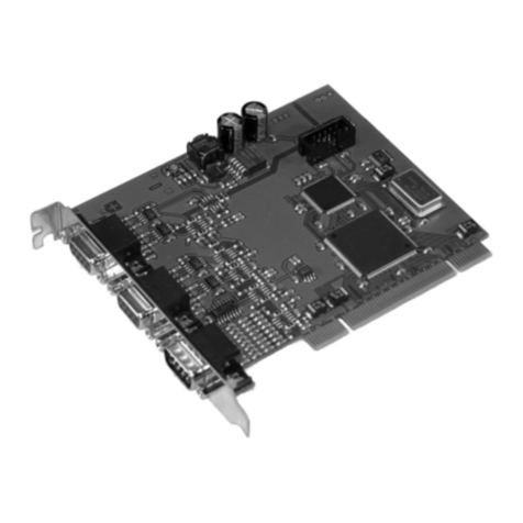
Prototype card PB751-AT provides means for development of custom cards for use in IBM
PC/XT and PC/AT or compatible computers. The card buffers all address lines, data lines,
and some of the control signals. It also provides address decoding for I/O addresses 000
through 3FF hex and for memory addresses 00000 through FF000 and, allows setup of the
selected address block size.
The PB751-AT card provides approximately 35 square inches of breadboard area for custom
circuit development. This breadboard area contains over 2600 plated-through holes for easy
component soldering. The holes are 0.035" in diameter with 0.100" spacing. The breadboard
area is surrounded by heavy buses for ground and +5VDC power.
The card is supplied with a 37-pin sub-D right angle connector and matching mounting
bracket. The properly spaced holes at the right end of the card will accommodate either one
37-pin sub-D connector, or one 25-pin and one 9-pin sub-D connector, or one 40, 50, or 60 pin
flat cable connector.
PC BUS PIN CONNECTIONS AND SIGNAL LIST
62-PIN CONNECTOR
Bracket End of Card
Ground B1 A1 < -IOCHCK
Reset < B2 A2 <> SD7
+5VDC B3 A3 <> SD6
IRQ2 > B4 A4 <> SD5
-5VDC B5 A5 <> SD4
DRQ1 > B6 A6 <> SD3
-12VDC B7 A7 <> SD2
-OWS > B8 A8 <> SD1
+12VDC B9 A9 <> SD0 C
S Ground B10 A10 < IO CH RDY O
O -SMEMW < B11 A11 < AEN M
L -SMEMR < B12 A12 <> SA19 P
D -IOW < B13 A13 <> SA18 O
E -IOR < B14 A14 <> SA17 N
R -DACK3 < B15 A15 <> SA16 E
DRQ3 > B16 A16 <> SA15 N
S -DACK1 < B17 A17 <> SA14 T
I DRQ1 > B18 A18 <> SA13
D -REFRESH < B19 A19 <> SA12 S
E CLK < B20 A20 <> SA11 I
IRQ7 > B21 A21 <> SA10 D
IRQ6 > B22 A22 <> SA9 E
IRQ5 > B23 A23 <> SA8
IRQ4 > B24 A24 <> SA7
IRQ3 > B25 A25 <> SA6
-DACK2 > B26 A26 <> SA5
T/C < B27 A27 <> SA4
BALE < B28 A28 <> SA3
+5VDC B29 A29 <> SA2
OSC B30 A30 <> SA1
Ground B31 A31 <> SA0

PB751-AT MANUAL FUNCTIONAL DESCRIPTION
Page 4MANUAL 00650-100-10
36-PIN CONNECTOR End Nearest to 62-Pin Connector
-MEM CS16 > D1 C1 > SBHE
-I/O CS16 > D2 C2 <> LA23 C
S IRQ10 > D3 C3 <> LA22 O
O IRQ11 > D4 C4 <> LA21 M
L IRQ12 > D5 C5 <> LA20 P
D IRQ15 > D6 C6 <> LA19 O
E IRQ14 > D7 C7 <> LA18 N
R -DACK0 < D8 C8 <> LA17 E
DRQ0 > D9 C9 > -MEMR N
S -DACK5 < D10 C10 > -MEMW T
I DRQ5 > D11 C11 <> SD08
D -DACK6 < D12 C12 <> SD09 S
E DRQ6 > D13 C13 <> SD10 I
-DACK7 < D14 C14 <> SD11 D
DRQ7 > D15 C15 <> SD12 E
+5VDC D16 C16 <> SD13
-MASTER D17 C17 <> SD14
Ground D18 C18 <> SD15
NOTES
1. > : Symbols pointing toward the connector designate signals into the card from devices
on the bus.
2. < : Symbols pointing away from the connector designate signals from the card to
devices on the bus.
3. <>: Double symbols indicate bi-directional signals.
4. A "minus" sign before the signal name signifies active low.
5. In the PC and PC/XT, the bus consists only of the 62-pin portion. Some of the signal
names are different but the functionality remains the same.
BUS SIGNAL LIST
The signal names used in this listing are for the AT Bus. When appropriate, the older names
used for the PC/XT are included in parenthesis. "I" indicates that the signal is an input from
the bus to the card and "O" signifies an output from the card to the bus. See the AT technical
manual for a more detailed description of these signals.
SIGNAL I/O DESCRIPTION
-OWS I
(or -ENDXFR) Zero Wait State. Fast bus devices pull this line low to prevent the
CPU from inserting extra wait cycles. The OWS signal tells the
microprocessor that it can complete the present bus cycle without
inserting any additional wait cycles.
AEN OAddress Enable. When this line is high, the DMA controller has
control of the address lines, data lines, memory read/write, and
I/O read/write.

PB751-AT MANUAL FUNCTIONAL DESCRIPTION
MANUAL 00650-100-10 Page 5
BALE
(ALE) OAddress Latch Enable. This line is used to latch valid addresses
and memory decodes from the microprocessor. It's available to
the I/O channel as an indicator of a valid microprocessor or DMA
address (when used with AEN). Microprocessor addresses SA0
through SA19 are latched with the falling edge of BALE. BALE is
forced high during DMA cycles.
CLK OSystem Clock. This clock signal may vary from 6 MHz to 8.33
MHz or higher.
-DACK1-7
(-DACK0-3) ODMA acknowledge lines used to acknowledge DMA requests
(DRQ). Active low.
DRQ0-7
(DRQ1-3) ODMA Request lines from devices on the bus that need DMA
service. The line must be held high until the corresponding
DACK line goes active (low). These lines are prioritized. DRQ0
has highest priority and DRQ7 has lowest priority. DRQ0
through DRQ3 perform 8-bit transfers and DRQ5 through DRQ7
perform 16 bit transfers. DRQ4 is not available on the I/O
channel.
-I/O CH CHKII/O Channel Check. When low, a device on the bus has detected a
parity error.
I/O CH RDY II/O Channel Ready. Pulled low (not ready) by a memory or I/O
device on the bus that needs more time. Never hold low for more
than 10 clock cycles (XT) or 2.5 usec (AT). Cycles are extended in
integral multiples of CLK cycles.
-I/O CS16 II/O 16-bit Chip Select. Signals a 16-bit one-wait-state I/O cycle.
This signal is active low and should be driven with an open
collector or tri-state driver capable of sinking 20 mA.
-IOR OI/O Read command. This line tells an I/O device on the bus to
drive its data onto the data bus. Active low.
-IOW OI/O Write command. This line instructs an I/O device on the bus
to read the data present on the data lines.
IRQ2-7, IRQ9-12,
& IRQ14-15 IInterrupt Request lines used by peripherals when they need
attention. Interrupt requests are prioritized with IRQ9 through
IRQ12 and IRQ14 through IRQ15 having the highest priority
(IRQ9 is the highest) and IRQ2 through IRQ7 having the lowest
priority (IRQ7 is the lowest). An interrupt line must be held high
until the microprocessor acknowledges the interrupt request
(Interrupt Service routine).
Interrupt 8 is used for the real time clock. Interrupt 13 is not
available on the I/O channel.
LA17-23 I/O Unlatched address lines valid when BALE is high. I/O devices
should latch these signals when BALE falls. Used for one wait-
state memory cycles.
-MASTER IA processor on the I/O channel may use this signal with a DRQ

PB751-AT MANUAL FUNCTIONAL DESCRIPTION
Page 6MANUAL 00650-100-10
to gain control of the address, data, and control lines of the bus.
The controlling processor may need to assume responsibility to
refresh system memory every 15 usec.
-MEM CS16 IMemory 16-Bit Chip Select signals a 16-bit, one-wait-state
memory cycle. This signal is active low and should be driven
with an open collector or tri state driver capable of sinking 20 mA.
-MEMR OMemory Read (AT). This signal tells bus memory devices to put
data onto the data bus. See -SMEMR to follow.
-MEMW OMemory Write (AT). This signal tells bus memory devices to put
the data onto the data bus. See -SMEMW to follow.
OSC OA 50% duty cycle clock signal with a frequency of 14.31818 MHz
-REFRESH OThis line is used in the AT to signal a memory refresh cycle. -
DACK0 is used for this purpose in the PC/XT. Active low.
RESET DRV OUsed to reset or initialize system logic on power-up or during low
line voltage. Synchronized to the falling edge of CLK.
SA0-19
(A0-19) OAddress lines for the first 1 MB of memory. SA0 is the
least significant bit (LSB).
SBHE OBus High Enable (system) indicates a 16 bit transfer of data.
SD0-15 I/O Data bits. SD0 is the least significant bit (LSB).
-SMEMR OMemory Read. This command tells memory on the bus to drive
its data onto the data bus. Used only with the lower 1 MB of
memory. Active low.
-SMEMW OMemory Write. This command instructs memory devices on the
bus to store the data present on the data bus. Used only on the
lower 1 MB of memory. Active low.
T/C OTerminal Count. This signal provides a pulse when the terminal
count for a DMA cycle is reached.
I/O ADDRESS MAP
The PB751-AT card address can be selected anywhere within the I/O address range 000-3FF
hex or the Memory address range 00000-FF000 providing that the address does not over lap
that of other installed functions. It is intended that I/O base addresses be selected at four-byte
intervals and that memory base address be selected at 4096 byte intervals.
Table 1 lists standard I/O address assignments.

PB751-AT MANUAL FUNCTIONAL DESCRIPTION
MANUAL 00650-100-10 Page 7
TABLE 1.
Hex Range Usage
000-00F DMA Chip 8237A-5
020-021 Interrupt 8259A
040-043 Timer 8253-5
060-063 PPI 8255A-5
080-083 DMA Page Register
0AX NMI Mask Register
0CX Reserved
0EX Reserved
100-1FF Not Usable
200-20F Game Control
210-217 Expansion Unit
220-24F Reserved
278-27F Reserved
2F0-2F7 Reserved
2F8-2FF Asynchronous Communication (secondary)
300-31F Prototype Card
320-32F Fixed Disk
378-37F Printer
380-38C** SDLC Communications
380-389** Binary Synchronous Comm. (secondary)
3A0-3A9 Binary Synchronous Comm. (primary)
3B0-3BF IBM Monochrome Display/Printer
3C0-3CF Reserved
3D0-3DF Color/Graphics
3E0-3E7 Reserved
3F0-3F7 Diskette
3F8-3FF Asynchronous Communication (primary)
** These options can not be used together - addresses over lap

PB751-AT MANUAL FUNCTIONAL DESCRIPTION
Page 8MANUAL 00650-100-10
This page intentionally left blank.

MANUAL 00650-100-10 Page 9
CHAPTER 3
ADDRESS SELECTION
The PB751-AT card address is set by DIP switch SW1. That switch controls I/O address bits
A2 through A9 if jumpers are installed between pins 1 and 2 of W1, W2, W3, W4, W5, W6, W7,
and W8. If those jumpers are installed between pins 2 and 3 at those locations, then the DIP
switch controls memory address bits A12 through A19.
In order to set the base address, first convert the desired hex address to binary form. Then, for
each "1" of the binary address, set the corresponding DIP switch to OFF and for each "0" of the
binary number, set the corresponding DIP switch to ON.
For example, to program a base address of hex 300 (11000000 binary) set switches A9 and A8 to
the OFF position and switches A7 through A2 to the ON position.
NOTE
Carefully review the Address Selection reference table on the previous page
before selecting the card address. If the address of two installed functions
overlaps you will experience unpredictable computer behavior.

PB751-AT MANUAL ADDRESS SELECTION
Page 10 MANUAL 00650-100-10
This page intentionally left blank.

MANUAL 00650-100-10 Page 11
CHAPTER 4
OPTION SELECTION
You can use the card as an I/O Card or as a Memory Card. Also, you can select the size of a
block of addresses reserved for this card. Base Address is set by DIP switches as described in
the previous section.
I/O Card or Memory Card
If the card will be used as an I/O card, place the jumper between the leftmost pins at the
location labeled I/O MEM. If the card is going to be used as a memory card, place that jumper
between the rightmost pins.
Jumpers W1, W2, W3, W4, W5, W6, W7, and W8 select either address lines A2 through A9 (if
the card is going to be an I/O card) or address lines A12 through A19 (if the card is going to be
a memory card) as input for the address decoding circuit. If the eight jumpers are installed
between the upper two pins, then I/O card addresses A2 through A9 are selected. If the
jumpers are installed between the lower two pins, then Memory addresses A12 through A19
are activated.
Block of Addresses Reserved
The size of a block of addresses reserved for the PB751-AT card is selected by the combination
of DIP switch settings just mentioned and jumpers marked 8, 16, 32, 32K, 64K, 128K, and 256K.
The jumper positions marked 8, 16, and 32 are primarily used to set I/O address space
required by the card. The remaining jumper positions are primarily used to set memory space
to be occupied by the card. If no jumpers are installed, then the block size is 4 Bytes for an I/O
card and 2K Bytes for a memory card. Refer to the following table:
I/O Card Memory Card Install
Address Space Address Space Jumpers
8 bytes 4K bytes * 8
16 bytes 8K bytes * 16
32 bytes 16K bytes * 32
64 bytes * 32K bytes 32K
128 bytes * 64K bytes 64K
256 bytes * 128K bytes 128K
512 bytes * 256K bytes 256K
Note: Selections marked "*" are infrequently used.
Base Address Selection When Address Blocks Are Reserved

PB751-AT MANUAL OPTION SELECTION
Page 12 MANUAL 00650-100-10
As described in the previous section of this manual, DIP switches A2 through A9 are used to
set the base address. The A2 position corresponds to the least significant bit of the address in
hexadecimal code and the A9 position corresponds to the most significant bit. If a block size of
four bytes is selected for an I/O card application (or 2K bytes for memory operation), then all
eight switches are available to set the base address. If one or more block reserving jumpers are
installed, then certain DIP switches MUST be placed in the off position as follows:
8 Bytes I/O or 4KB Memory: A2 must be OFF
16 Bytes I/O or 8KB Memory: A2 AND A3 must be OFF
32 Bytes I/O or 16KB Memory: A2, A3 AND A4 must be OFF
64 Bytes I/O or 32KB Memory: A2, A3, A4 AND A5 must be OFF
128 Bytes I/O or 64KB Memory: A2, A3, A4, A5, AND A6 must be OFF
256 Bytes I/O or 128KB Memory: A2, A3, A4, A5, A6 AND A7 must be OFF
512 Bytes I/O or 256KB Memory: A2, A3, A4, A5, A6, A7 AND A8 must be OFF
Eight or 16-bit Operation
For 16-bit operation, it is necessary to complete wiring on IC U7 and to add a 74LS125 as
shown within dotted lines on the schematic. Further, you may require different or additional
circuitry depending on how you wish this card to interface to the computer I/O bus.

MANUAL 00650-100-10 Page 13
CHAPTER 5
SPECIFICATIONS
Computer Connector: Gold edge connector for IBM PC/XT,PC/AT, or compatible
computers.
Breadboard Area: Approximately 35 square inches with 0.035" plated-through holes
spaced 0.100" apart. Heavy ground and +5VDC buses surround
the breadboard area.
Address Signals: Address lines are buffered by type 74LS244 line drivers, labeled,
and available at assigned pads. See Schematic.
Data Signals: Data lines D0 through D15 are buffered by two type 74LS245
transceiver, and are available at assigned pads. See Schematic.
Address Decode: Decoding provided for either I/O addresses or for Memory
addresses. Card address is DIP switch selectable.
Card Address Block: Jumper selectable; 8, 16, or 32 bytes for I/O card use and 32K,
64K,128K, or 256K for Memory card use.
Output Connector: A 37-pin Sub-D right angle connector and mounting bracket are
included. Properly spaced holes are provided for other
combinations of connectors such as 9-pin Sub-D plus 25-pin Sub-
D. The card will also accept 50-pin ribbon cable connectors.
Bracket: Mounting bracket for standard 37-pin Sub-D connector included.
Card Size: Full size PC/XT card (13.25" x 3.87")
Operating Temperature: 0 to +60oC.
Storage Temperature: -20 to +85oC.
Humidity: 5% to 95% RH, non-condensing.
Table of contents
Other ICS Advent PCI Card manuals

ICS Advent
ICS Advent PCI-32REL User manual

ICS Advent
ICS Advent AOB8/16 User manual

ICS Advent
ICS Advent ADIO1600 Series User manual

ICS Advent
ICS Advent PCI-ICOM485/4 User manual

ICS Advent
ICS Advent ULTRA-485 User manual

ICS Advent
ICS Advent WDT1000-P User manual

ICS Advent
ICS Advent RB-24 User manual

ICS Advent
ICS Advent DUAL232/AT Series User manual

ICS Advent
ICS Advent WINCOMM8/C User manual

ICS Advent
ICS Advent PCI-DIO48 Series User manual