IDT CPS-16 User manual

July 10, 2012
IDTCPS-16/12/8
Central Packet Switch
User Manual
Revision 1.5
Tit

GENERAL DISCLAIMER
Integrated Device Technology, Inc. (“IDT”) reserves the right to make changes to its products or specifications at any time, without notice, in order to improve design or perfor-
mance. IDT does not assume responsibility for use of any circuitry described herein other than the circuitry embodied in an IDT product. Disclosure of the information herein
does not convey a license or any other right, by implication or otherwise, in any patent, trademark, or other intellectual property right of IDT. IDT products may contain errata
which can affect product performance to a minor or immaterial degree. Current characterized errata will be made available upon request. Items identified herein as “reserved”
or “undefined” are reserved for future definition. IDT does not assume responsibility for conflicts or incompatibilities arising from the future definition of such items. IDT products
have not been designed, tested, or manufactured for use in, and thus are not warranted for, applications where the failure, malfunction, or any inaccuracy in the application
carries a risk of death, serious bodily injury, or damage to tangible property. Code examples provided herein by IDT are for illustrative purposes only and should not be relied
upon for developing applications. Any use of such code examples shall be at the user's sole risk.
Copyright © 2012 Integrated Device Technology, Inc.
All Rights Reserved.
The IDT logo is registered to Integrated Device Technology, Inc. IDT and CPS are trademarks of Integrated Device Technology, Inc.

Revision 1.5
Integrated Device Technology, Inc.
CPS-16/12/8 User Manual iii July 10, 2012
1 Device Overview.......................................................................................................................1-1
1.1 Device Description .......................................................................................................1-1
1.2 Key Features................................................................................................................1-2
1.3 Additional Resources ...................................................................................................1-2
1.4 Block Diagram..............................................................................................................1-3
1.5 Application Example: The Wireless Basestation..........................................................1-4
1.6 Functional Overview ....................................................................................................1-5
1.7 Functional Differences with PPS-Gen2 (80KSW0001) ................................................1-5
2 sRIO Ports ................................................................................................................................2-1
2.1 sRIO Port Definition .....................................................................................................2-1
2.2 Trace Function .............................................................................................................2-3
2.3 Packet Filtering ............................................................................................................2-7
2.4 Software Assisted Error Recovery ...............................................................................2-7
3 Switch Description ....................................................................................................................3-1
3.1 Conceptual Functionality..............................................................................................3-1
3.2 Switching Block and Elements.....................................................................................3-1
3.3 Switch Description .......................................................................................................3-2
3.4 Switching Scheduler and Priorities ..............................................................................3-3
3.5 Flow Control and Congestion Management.................................................................3-5
4 I2C Interface .............................................................................................................................4-1
4.1 Overview ......................................................................................................................4-1
4.2 Master/Slave Configuration..........................................................................................4-1
4.3 Temporary Master Mode ..............................................................................................4-1
4.4 Slave Mode ..................................................................................................................4-7
5 Error Management....................................................................................................................5-1
5.1 Error Management Functional Architecture ................................................................5-1
6 JTAG & Boundary Scan............................................................................................................6-1
6.1 JTAG and AC Extest Compliance ................................................................................6-1
6.2 Test Instructions ...........................................................................................................6-1
6.3 Device ID Register.......................................................................................................6-2
6.4 Initialization and Reset.................................................................................................6-2
6.5 Configuration Register Access.....................................................................................6-2
6.6 Boundary Scan ............................................................................................................6-3
7 Reference Clock .......................................................................................................................7-1
7.1 Reference Clock Specification .....................................................................................7-1
7.2 PLL...............................................................................................................................7-1
8 Programming the Device ..........................................................................................................8-1
8.1 Device Access .............................................................................................................8-1
8.2 Route Tables ................................................................................................................8-3
8.3 Device Programming ...................................................................................................8-9
8.4 Example of Programming ..........................................................................................8-12
8.5 Optional API Calls......................................................................................................8-13
Contents

IDT Table of Contents
Revision 1.5
Integrated Device Technology, Inc.
CPS-16/12/8 User Manual iv July 10, 2012
9 Reset & Initialization.................................................................................................................9-1
9.1 Registers......................................................................................................................9-1
9.2 Initialization Steps........................................................................................................9-2
9.3 Initialization of RIO Ports .............................................................................................9-2
9.4 RIO System Bring Up...................................................................................................9-2
9.5 Serdes Initialization......................................................................................................9-2
10 Registers ...............................................................................................................................10-1
10.1 RapidIO Compliance..................................................................................................10-1
10.2 Register Type Field Definitions ..................................................................................10-1
10.3 Address Map..............................................................................................................10-2
10.4 Rapid IO Registers.....................................................................................................10-8
10.5 RIO extended feature registeR ................................................................................10-19
10.6 IDT Specific sRIO Extended Feature Set ................................................................10-24
10.7 Routing Table Registers...........................................................................................10-25
10.8 Trace Registers........................................................................................................10-26
10.9 Global Configuration Registers................................................................................10-31
10.10 Multicast Registers...................................................................................................10-38
10.11 Switching Port Registers..........................................................................................10-40
10.12 Error Registers.........................................................................................................10-47
10.13 QUAD Control Registers..........................................................................................10-52
11 References ............................................................................................................................ 11-1

Revision 1.5
Integrated Device Technology, Inc.
CPS-16/12/8 User Manual v July 10, 2012
Figure 1.1 Block Diagram ..................................................................................................................1-3
Figure 1.2 CPS Interconnect..............................................................................................................1-4
Figure 1.3 Application Overview ........................................................................................................1-4
Figure 2.1 Trace Matching Criteria ....................................................................................................2-4
Figure 2.2 Illustration of the Trace Function within a Given Port .......................................................2-5
Figure 3.1 CPS Switch Core Block Diagram......................................................................................3-1
Figure 3.2 Input Buffer Diagram.........................................................................................................3-2
Figure 4.1 Bit Transfer on the I2C Bus ..............................................................................................4-8
Figure 4.2 START and STOP Signaling ............................................................................................4-8
Figure 4.3 Data Transfer....................................................................................................................4-9
Figure 4.4 Acknowledgment ..............................................................................................................4-9
Figure 4.5 Master Addressing a Slave with a 7-bit Address (Transfer Direction is Not Changed) ....4-9
Figure 4.6 Master Reads a Slave Immediately After the First Byte ...................................................4-9
Figure 4.7 Combined Format...........................................................................................................4-10
Figure 4.8 Master Addresses a Slave-Receiver with 10-bit Address...............................................4-10
Figure 4.9 Master Addresses a Slave Transmitter with 10-bit Address ...........................................4-10
Figure 4.10 Combined Format: Master Addresses a Slave with 10-bit Address ...............................4-10
Figure 4.11 Combined Format: Master Transmits Data to Two Slaves, Both with 10-bit Address ....4-11
Figure 4.12 Write Protocol with 10-bit Slave Address (ADS is 1) ......................................................4-12
Figure 4.13 Read Protocol with 10-bit Slave Address (ADS is 1)......................................................4-12
Figure 4.14 Write Protocol with 7-bit Slave Address (ADS is 0) ........................................................4-12
Figure 4.15 Read Protocol with 7-bit Slave Address (ADS is 0)........................................................4-13
Figure 5.1 Functional View of Error Management Block....................................................................5-1
Figure 6.1 JTAG Write Access...........................................................................................................6-3
Figure 6.2 JTAG Read Access ..........................................................................................................6-3
Figure 7.1 Reference Clock Representative Circuit...........................................................................7-1
Figure 7.2 Internal PLL Clock Generator ...........................................................................................7-2
Figure 8.1 Route Table Lookup Diagram...........................................................................................8-3
Figures

Revision 1.5
Integrated Device Technology, Inc.
CPS-16/12/8 User Manual vi July 10, 2012
Table 2.1 Port Numbering.................................................................................................................. 2-1
Table 2.2 Port Configuration Examples............................................................................................. 2-2
Table 4.1 EEPROM Register Address Map....................................................................................... 4-3
Table 4.2 Register Map Example ...................................................................................................... 4-5
Table 4.3 EEPROM Format Example................................................................................................ 4-6
Table 4.4 I2C Address Pins............................................................................................................... 4-7
Table 5.1 Error Sources and Codes .................................................................................................. 5-1
Table 5.2 I2C Errors and Codes -- Group Number 0x1..................................................................... 5-2
Table 5.3 JTAG Errors and Codes -- Group Number 0x2.................................................................. 5-3
Table 5.4 Maintenance Handler Errors and Codes -- Group Number 0x3 ........................................ 5-4
Table 5.5 Configuration Errors and Codes -- Group Number 0x5 ..................................................... 5-5
Table 5.6 RIO SERDES Errors and Codes -- Group Number 0x6 .................................................... 5-6
Table 5.7 RIO Link Layer Errors and Codes -- Group Number 0x7................................................... 5-6
Table 5.8 RIO Link Protocol Errors and Codes -- Group Number 0x8 .............................................. 5-7
Table 5.9 RIO Logical and Transport Errors and Codes -- Group Number 0x9................................. 5-8
Table 5.10 Port Write Payload Definition............................................................................................5-11
Table 5.11 Maintenance Packet Format.............................................................................................5-11
Table 6.1 Test Instructions................................................................................................................. 6-1
Table 6.2 Configuration Registers ..................................................................................................... 6-2
Table 8.1 RIO Defined Maintenance Packet with CPS as Destination.............................................. 8-1
Table 8.2 RIO Defined Maintenance Response Packet generated by CPS...................................... 8-2
Table 8.3 Port Configuration.............................................................................................................. 8-4
Table 8.4 Multicast Mask Register References for Multicast Mask Port CSR Usage........................ 8-6
Table 8.5 Region Select .................................................................................................................... 8-7
Table 8.6 Port Number References................................................................................................... 8-7
Table 8.7 Multicast Mask References................................................................................................ 8-8
Table 9.1 Port Configuration at Power Up.........................................................................................9-1
Table 9.2 Default Speed Settings with SPD0 and SPD1................................................................... 9-2
Table 10.1 Register Types................................................................................................................. 10-1
Table 10.2 CPS Memory Map ........................................................................................................... 10-2
Table 10.3 DEV_IDENT_CAR 0x000000 .......................................................................................... 10-8
Table 10.4 DEV_INF_CAR 0x000004 ............................................................................................... 10-8
Table 10.5 ASSY_IDENT_CAR 0x000008........................................................................................ 10-9
Table 10.6 ASSY_INF_CAR 0x00000C ............................................................................................ 10-9
Table 10.7 PROC_ELEM_FEAT_CAR 0x000010 ........................................................................... 10-10
Table 10.8 SWITCH_PORT_INF_CAR 0x000014 ...........................................................................10-11
Table 10.9 SRC_OPS_CAR 0x000018 ........................................................................................... 10-12
Table 10.10 SW_MCAST_SUP_CAR 0x000030............................................................................... 10-13
Table 10.11 SW_RTE_TBL_LIM_CAR 0x000034............................................................................. 10-14
Table 10.12 SW_MULT_INF_CAR 0x000038 ................................................................................... 10-14
Table 10.13 HOST_BASE_DEV_ID_LOCK_CSR 0x000068 ............................................................ 10-14
Table 10.14 COMPONENT_TAG_CSR 0x00006C ........................................................................... 10-15
Table 10.15 STD_RTE_CONF_DESTID_SEL_CSR 0x000070........................................................ 10-15
Table 10.16 STD_RTE_CONF_PORT_SEL_CSR 0x000074 ........................................................... 10-16
Table 10.17 STD_RTE_DEFAULT_PORT 0x000078........................................................................ 10-16
Table 10.18 MCAST_MASK_PORT 0x000080 ................................................................................. 10-17
Table 10.19 MCAST_ASSOC_SEL_CSR 0x000084 ........................................................................ 10-17
Table 10.20 MCAST_ASSOC_OP_CSR 0x000088 .......................................................................... 10-18
Table 10.21 PORT_MAINT_BLOCK_HEAD 0x000100..................................................................... 10-18
Tables

IDT List of Tables
Revision 1.5
Integrated Device Technology, Inc.
CPS-16/12/8 User Manual vii July 10, 2012
Table 10.22 PORT_LINK_TO_CTRL_CSR 0x000120...................................................................... 10-18
Table 10.23 PORT_GEN_CTRL_CSR 0x00013C............................................................................. 10-19
Table 10.24 RIO Extended Register Map.......................................................................................... 10-19
Table 10.25 PORT_0_LINK_MAINT_REQ_CSR 0x000140 ............................................................. 10-20
Table 10.26 PORT_0_LINK_MAINT_RESP_CSR 0x000144 ........................................................... 10-20
Table 10.27 PORT_0_LOCAL_ACKID_CSR 0x000148.................................................................... 10-21
Table 10.28 PORT_0_ERR_STAT_CSR 0x000158 .......................................................................... 10-22
Table 10.29 PORT_0_CTRL_CSR 0x00015C .................................................................................. 10-22
Table 10.30 LOCAL_RTE_CONF_DESTID_SEL_CSR 0x010070 ................................................... 10-24
Table 10.31 Routing Table Register .................................................................................................. 10-25
Table 10.32 Route Table Register 0xE00000-0xE1F7FC.................................................................. 10-25
Table 10.33 Trace Register Map ....................................................................................................... 10-26
Table 10.34 Port_0_Trace_Value_1_Block_0 0xE40000 .................................................................. 10-27
Table 10.35 Port_0_Trace_Value_1_Block_1 0xE40004 .................................................................. 10-27
Table 10.37 Port_0_Trace_Value_1_Block_3 0xE4000C.................................................................. 10-28
Table 10.36 Port_0_Trace_Value_1_Block_2 0xE40008 .................................................................. 10-28
Table 10.39 Port_0_Mask_Value_1_Block_0 0xE40014................................................................... 10-29
Table 10.38 Port_0_Trace_Value_1_Block_4 0xE40010 .................................................................. 10-29
Table 10.41 Port_0_MASK_Value_1_Block_2 0xE4001C ................................................................ 10-30
Table 10.42 Port_0_Mask_Value_1_Block_3 0xE40020................................................................... 10-30
Table 10.40 Port_0_MASK_Value_1_Block_1 0xE40018................................................................. 10-30
Table 10.44 CPS_CONTROL 0xF2000C .......................................................................................... 10-31
Table 10.43 Port_0_Mask_Value_1_Block_4 0xE40024................................................................... 10-31
Table 10.45 CONF_MOD_ERR_REPORT_ENABLE 0xF20014 ...................................................... 10-32
Table 10.46 AUXPORT_ERR_REPORT_ENABLE 0xF20018.......................................................... 10-33
Table 10.47 MAINT_ERR_REPORT_ENABLE 0xF2001C ............................................................... 10-33
Table 10.48 RIO_DOMAIN 0xF20020............................................................................................... 10-33
Table 10.49 RIO_PORT_WRITE_INFO 0xF20024 ........................................................................... 10-34
Table 10.50 RIO_PORT_WRITE_SRCID 0xF20028......................................................................... 10-34
Table 10.51 RIO_ASSY_IDENT_CAR 0xF2002C............................................................................. 10-35
Table 10.52 RIO_ASSY_INF_CAR 0xF20030 .................................................................................. 10-35
Table 10.53 PPS_SOFT_RESET 0xF20040..................................................................................... 10-35
Table 10.54 I2C_MASTER_CTRL 0xF20050.................................................................................... 10-36
Table 10.55 I2C_MASTER_STAT_CTRL 0xF20054 ......................................................................... 10-37
Table 10.56 MULTICAST Register Map ............................................................................................ 10-38
Table 10.57 MULTICAST0 0xF30000................................................................................................ 10-39
Table 10.58 Switching Port Register Map ......................................................................................... 10-40
Table 10.59 PORT_0_BUF_SIZE 0xF40000..................................................................................... 10-41
Table 10.60 PORT_0_OPS 0xF40004 .............................................................................................. 10-41
Table 10.61 PORT_0_ERR_REPORT_ENABLE 0xF40008............................................................. 10-43
Table 10.62 PORT_0_SWITCH_BUF_STATUS 0xF4000C .............................................................. 10-44
Table 10.63 PORT_0_ACK_CNTR 0xF40010 .................................................................................. 10-44
Table 10.64 PORT_0_NACK_CNTR 0xF40014................................................................................ 10-45
Table 10.65 PORT_0_SW_PKT_CNTR 0xF4001C .......................................................................... 10-45
Table 10.66 PORT_0_TRACE_MATCH_CNTR_1 0xF40020........................................................... 10-45
Table 10.67 PORT_0_TRACE_MATCH_CNTR_2 0xF40024........................................................... 10-45
Table 10.68 PORT_0_TRACE_MATCH_CNTR_3 0xF40028........................................................... 10-46
Table 10.69 PORT_0_TRACE_MATCH_CNTR_4 0xF4002C .......................................................... 10-46
Table 10.70 PORT_0_FILTER_MATCH_CNTR_1 0xF40030 ........................................................... 10-46
Table 10.71 PORT_0_FILTER_MATCH_CNTR_2 0xF40034 ........................................................... 10-46
Table 10.72 PORT_0_FILTER_MATCH_CNTR_3 0xF40038 ........................................................... 10-47
Table 10.73 PORT_0_FILTER_MATCH_CNTR_4 0xF4003C........................................................... 10-47
Table 10.74 ERR_CAP_REG 0xFD0000 .......................................................................................... 10-47
Table 10.75 ERR_LOG_RD 0xFD0004............................................................................................. 10-48
Table 10.76 SPECIAL_ERR Register Map........................................................................................ 10-48

IDT List of Tables
Revision 1.5
Integrated Device Technology, Inc.
CPS-16/12/8 User Manual viii July 10, 2012
Table 10.77 SPECIAL_ERR_0 0xFD0008 ........................................................................................ 10-48
Table 10.78 ERR_FLAG 0xFD0028 .................................................................................................. 10-50
Table 10.79 ERR_COUNTER 0xFD002C ......................................................................................... 10-50
Table 10.80 ERR_RESET 0xFD0030................................................................................................ 10-51
Table 10.81 QUAD_CTRL Control Register Map.............................................................................. 10-52
Table 10.82 QUAD_0_CTRL 0xFF0000............................................................................................ 10-52
Table 10.83 QUAD_0_ERR_REPORT_EN 0xFF0004...................................................................... 10-54
Table 10.84 QUAD_CTRL_BROADCAST 0xFFF000 ....................................................................... 10-54

Revision 1.5
Integrated Device Technology, Inc.
CPS-16/12/8 User Manual ix July 10, 2012
Introduction
This user reference manual includes hardware and software information for the CPS family products. It
applies to CPS-16, CPS-12, and CPS-8. The only deference is port number, device ID and register map file.
The pinout is covered in each individual datasheet. All the description through out the user manual is
default as CPS-16. The register file of CPS-12 and CPS-8 is a subset of CPS-16, the registers associated
with invalid port/quad are treated as reserved.
DEVICE ID: CPS-16 device ID is 0x35B, CPS-12 device ID is 0x35D, CPS-8 device ID is 0x35C.
PORT/QUAD NUMBER: CPS-16 has 4 QUAD provides up to 16 ports. CPS-12 has 3 QUAD pro-
vides up to 12 ports. CPS-8 has 2 QUAD provides up to 8 ports.
Content Summary
Chapter 1, “CPS Device Overview,” provides a complete introduction to the capabilities of the CPS. It
includes the major difference from PPS device.
Chapter 2, “Serial RapidIO Ports,” covers the device’s Serial RapidIO ports. These ports are RapidIO
specification 1.3 compliant. Also covers IDT specific features such as tracing and filtering.
Chapter 3, “CPS Switch Description,” covers the switch core behavior and flow control mechanism.
Chapter 4, “I2C Bus Interface,” describes the standard I2C bus interface implemented on the CPS.
Chapter 5, “Error Management,” explains the CPSs Error Management block. This block is responsible
for receiving, filtering, logging, counting, and responding to error reports from all of the functional blocks
within the device.
Chapter 6, “JTAG & Boundary Scan,” describes the CPS JTAG interface and code.
Chapter 7, “Reference Clock,” describes the reference clock requirement, system clock and SerDes clock
generation.
Chapter 8, “Programming the CPS,” provides the basic configure steps and rules.
Chapter 9, “CPS Reset & Initialization” provides reset and init steps.
Chapter 10, “Registers” provides the full memory map and complete listing of the CPS-16 registers,
register type, register fields, and their respective addresses. CPS-8 is a subset of CPS-16.
Chapter 11, “References,” provides a list of all associated specifications referred to in this manual.
Documentation Conventions and Definitions
Throughout this manual the following conventions and terms are used:
To define the active polarity of a signal, signal names with and without overbars will be used. Signal
names with overbars are considered negative polarity or “active low” and are thus enabled when a
low voltage is applied.
To define buses, the most significant bit (MSB) will be on the left and least significant bit (LSB) will
be on the right. No leading zeros will be included.
To represent numerical values, either decimal, binary, or hexadecimal formats will be used. The
binary format is as follows: 0bDDD, where “D” represents either 0 or 1; the hexadecimal format is
as follows: 0xDD, where “D” represents the hexadecimal digit(s); otherwise, it is decimal.
Unless otherwise denoted, a byte will refer to an 8-bit quantity. A word will refer to a 32-bit quantity,
and a double word will refer to an 8 Byte (64-bit) quantity. This is in accordance with RapidIO con-
About This Manual

IDT About This Manual
Revision 1.5
Integrated Device Technology, Inc.
CPS-16/12/8 User Manual x July 10, 2012
vention.
A bit is set when its value is 0b1. A bit is cleared when its value is 0b0.
The compressed notation ABC[x|y|z]D refers to ABCxD, ABCyD, and ABCzD.
The compressed notation ABC[x..y]D refers to ABCxD, ABC(x+1)D, ABC(x+2)D,... ABCyD.
In double words, bit 63 is always the most significant bit and bit 0 is the least significant bit. In
words, bit 31 is always the most significant bit and bit 0 is the least significant bit. In bytes, bit 7 is
always the most significant bit and bit 0 is the least significant bit.
This device follows the Big endian convention. The ordering of bytes within words is referred to as
either “big endian” or “little endian.” Big endian systems label byte zero as the most significant (left-
most) byte of a word. Little endian systems label byte zero as the least significant (rightmost) byte
of a word.
Figure 1 Example of Byte Ordering for “Big Endian” or “Little Endian” System Definition
A read-only: register, bit, or field is one which can be read but not modified
A sticky bit is a bit that remains set after being set by hardware until a zero is written to it. Writing a
one to a sticky has no effect on its value.
A zero field in a register, denoted as “0” in register figures, must be written with a value of zero and
returns a value of zero when read.
Revision History
July 10, 2012: Revision 1.5. Removed the confidential statements from the document’s footers.
January 19, 2011: Revision 1.4. Fixed a number of minor errors, updated I2C Interface, and added
notes to Packet Filtering and Multicast Packets
May 21, 2009: Revision 1.3. Fixed a number of minor errors.
January 19, 2009: Revision 1.2.
1. Add more detail about the Ack Counter and Nack Counter
2. Add basic device Programming example
3. Add detail explanation about the multicast respond
4. Add explanation about the multicast with responds
5. Add EPROM format example.
June 9, 2008: Revision 1.1.
Corrected switch chapter text around number of retries allowed for CRC error, as well as multicast
delaying discussion. Fixed /IRQ polarity in Error Handling chapter. Other editorial changes.
September 7, 2007: Initial release. Revision 1.0.
0123
bit 0bit 31
Address of Bytes within Words: Big Endian
3210
bit 0bit 31
Address of Bytes within Words: Little Endian

Revision 1.5
Integrated Device Technology, Inc.
CPS-16/12/8 User Manual 1 - 1 July 10, 2012
Chapter 1
Device Overview
1 DEVICE OVERVIEW
The objective of this chapter is to provide an overview of the capabilities of the CPS device.
1.1 DEVICE DESCRIPTION
The CPS device functionality is optimized for line card and backplane switching. Its primary function is to
switch data plane and control plane data packets via Serial Rapid IO (SRIO) between a set of devices that
reside on the same line card. In addition, it supports the ability to bridge communications between multiple
on-board (or local) devices and a set of external line cards by providing long run Rapid IO backplane inter-
connects. In this manner, for example, the device can serve as a switch between a set of RF cards and a
set of Rapid IO based DSPs in a wireless basestation.
The CPS device supports packet switching from up to 16 ports which are comprised of 16 SRIO Lanes. The
encoded data rate for each of the lanes are configurable to either 1.25 Gbps, 2.5 Gbps, or 3.125 Gbps. The
device supports lane grouping such that both 1x and 4x operation, as defined in the applicable RIO specifi-
cations. In addition, the device supports lane grouping in an “enhanced” mode such that a group of 4 Lanes
can be configured as four individual non-redundant 1x ports.
The CPS device supports the reception of SRIO maintenance packets (type 8) which are directed to it (i.e.
hop count of 0) in support of requirements defined for a RIO switch in the applicable version 1.3 Rapid IO
specifications. The CPS device supports the ability to properly process and forward received maintenance
packets with a hop count >0 as defined in the Rapid IO specifications. With the exception of maintenance
packets, received packets are transmitted unmodified as defined in the 1.3 versions of the applicable Rapid
IO specifications.
From a switching perspective the device functions statically. As such, all input to output port mappings are
configurable through registers. Unless register configurations are changed, the input to output mappings
remains static regardless of the received data (disregarding errors). The switching functionality does not
dynamically “learn” which destinationIDs are tied to a given port by examining RIO header fields and
dynamically updating internal routing tables.
The device supports priority levels 0 - 3 as defined in the revision 1.3 Rapid IO specifications.
The CPS device is programmable by RIO ports, I2C JTAG interface.

IDT Device Overview
Revision 1.5
Integrated Device Technology, Inc.
CPS-16/12/8 User Manual 1 - 2 July 10, 2012
1.2 KEY FEATURES
Interfaces - sRIO
–Up to 16/12/8 Serial RapidIO (sRIO) v1.3 full duplex lanes, supporting 4x-ports, 1x-ports, or combi-
nations thereof
–Lane Rates selectable; 3.125Gbps, 2.5Gbps, or 1.25Gbps
–Short- or Long-haul reach for each Lane at all rates
–Both pre-emphasis and drive strength
–Software assisted error recovery supports hot swap
Interfaces - I2C
–A single I2C interface either in master mode or slave mode
–Hardware pin configurable address
–Power up booting from external I2C memory device with error checking and reporting
Switch
–Peak throughput 40Gbps (CPS-16), 30Gbps (CPS-12), and 20Gbps (CPS-8)
–Support cut-through mode
–Per priority buffering
–Support 4 RIO priorities
–Non head of line blocking
–Support Multicast control symbol
–Support Broadcast
–10 Multicast mask
–Per port independent routing table
Packet Trace
–Each Port provides the ability to match the first 160 bits of any packet against up to four program-
mable values as comparison criteria to copy the packet to a programmable output trace port
Clock and reset
–Single input reference clock
–Global hardware reset
–Software reset
Diagnostic packet counters
Power Dissipation
–CPS-16 maximum power consumption is 3.2W
–CPS-12 maximum power consumption is 2.8W
–CPS-8 maximum power consumption is 2.4W
Full JTAG Boundary Scan Support (IEEE1149.1 & 1149.6)
Package:
–FCBGA 324-ball grid array, 19 mm x 19 mm, 1.0 mm ball pitch
1.3 ADDITIONAL RESOURCES
In addition to this User’s Reference Manual, which explains the functionality of the CPS and how to use the
device. There is the device’s datasheet which covers all electrical specifications, package pinouts, and ther-
mal characteristics available on IDT’s secure access site. Contact your local IDT sales representative to
obtain your copy.

IDT Device Overview
Revision 1.5
Integrated Device Technology, Inc.
CPS-16/12/8 User Manual 1 - 3 July 10, 2012
1.4 BLOCK DIAGRAM
Figure 1.1 Block Diagram
Register
File
Maintenance
&
Error
Management
JTAG
I2C
SRIO
Quad 0
Logical
SRIO
SERDES
Lane 0
SRIO
SERDES
Lane 1
SRIO
SERDES
Lane 2
SRIO
SERDES
Lane 3
SRIO
Quad 1
Logical
SRIO
SERDES
Lane 4
SRIO
SERDES
Lane 5
SRIO
SERDES
Lane 6
SRIO
SERDES
Lane 7
SRIO
Quad 2
Logical
SRIO
SERDES
Lane 8
SRIO
SERDES
Lane 9
SRIO
SERDES
Lane 10
SRIO
SERDES
Lane 11
SRIO
Quad 3
Logical
SRIO
SERDES
Lane 12
SRIO
SERDES
Lane 13
SRIO
SERDES
Lane 14
SRIO
SERDES
Lane 15
IDT Device Overview
Revision 1.5
Integrated Device Technology, Inc.
CPS-16/12/8 User Manual 1 - 4 July 10, 2012
Figure 1.2 CPS Interconnect
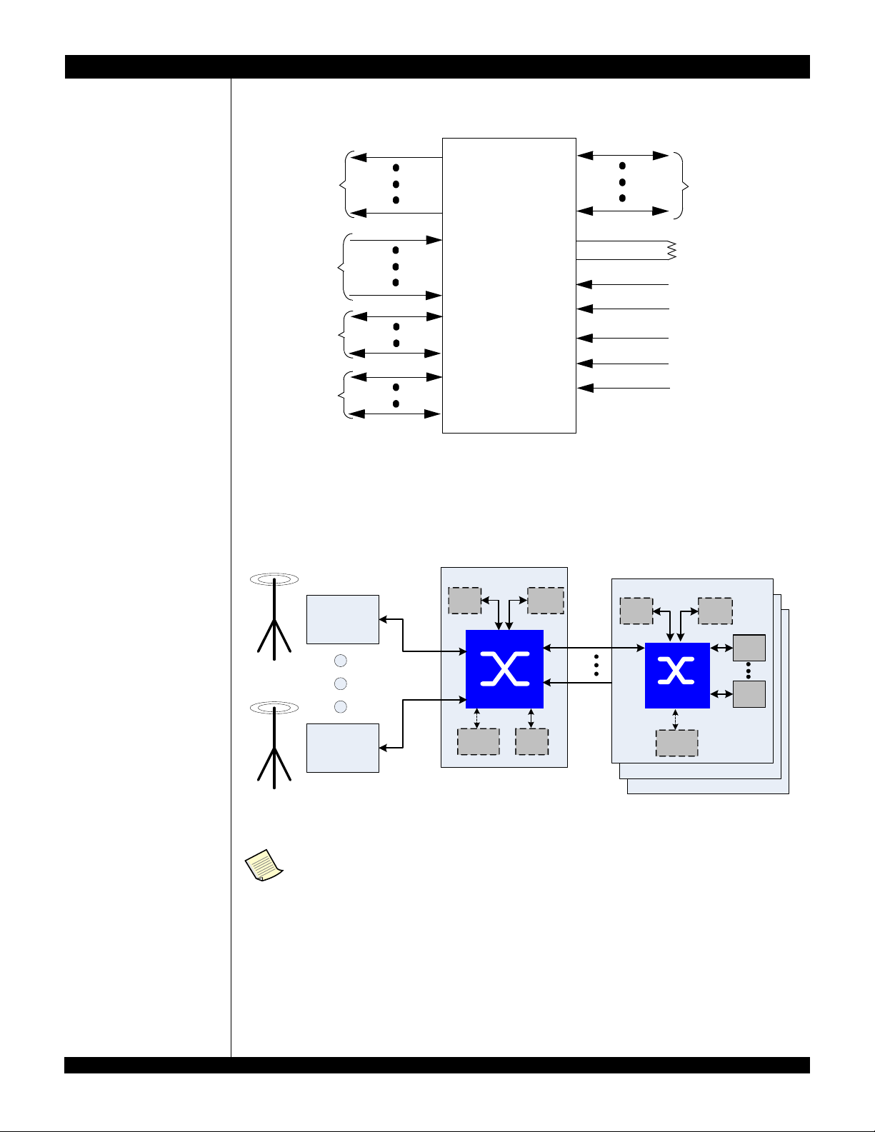
1.5 APPLICATION EXAMPLE: THE WIRELESS BASESTATION
Central switch based wireless processing
Figure 1.3 Application Overview
In a macro wireless station, a switch-based raw data combination and distribution architecture is widely
adopted. Switch based architecture provides high flexibility and high resource efficiency. The raw data from
the Radio Unit is distributed to one or more processing cards by unicast or multicast. Aggregating raw data
from processing cards to a buffer-less chain can be done by a fast non-blocking switch. It’s also suitable in
processing card since more and more processing is moved from RNC to Node B in the emerging applica-
tions.
The CPS provides direct support for backplane connections using the serial RapidIO standard.
The addition of an appropriate bridge (e.g., CPRI to sRIO) allows for further backplane flexibility,
accommodating designs based on a wide range of standards such as CPRI, OBSAI, GbE, or
PCIe.
CPS
SRIO Tx
Differential
x16
SRIO Rx
Differential
x16
I2C Interface
14 Signals
SERDES
Drive Bias
12 K ohm
RIO
Speed
Select
JTAG Reset Signal
System
Clock
Tes t
Signals
(or x8, x12)
(or x8, x12)
RF Element
RF Element
CPU FPGA
CPS-16
Serial RapidIO
CPS-8
Serial
RapidIO
DSP
DSP
CPU FPGA
1
PROM
Central Switch Board(s)
I2C
PROM
I2C
Baseband Board(s)
DSP
1
2
… N

IDT Device Overview
Revision 1.5
Integrated Device Technology, Inc.
CPS-16/12/8 User Manual 1 - 5 July 10, 2012
1.6 FUNCTIONAL OVERVIEW
The user may program IDT’s CPS to direct incoming packet data with a given destination ID to a packet
processor. Input packets are switched as defined by the transport layer of RIO specification. The CPS
receives the packets from up to 16 unique ports, the received packets may be processed in three ways:
a. Multicast:If a Multicast ID is received, the CPS performs a multicast as defined by the
device’s configurable RIO multicast mask registers.
b. Unicast: it is performed as specified in RIO.
c. Maintenance packets: As specified in sRIO
1.7 FUNCTIONAL DIFFERENCES WITH PPS-GEN2 (80KSW0001)
1.7.1 Enhanced Queue
It can bypass the congested head in the queue.
1.7.2 Port/Lane Count
The CPS family device provides 16/12/8 sRIO lanes which can be configured into up to 16/12/8 ports. The
80KSW0001 provides up to 12 ports
1.7.3 Bandwidth
CPS provides a 40/30/20 Gbps bandwidth.
1.7.4 PPSc Capability
The CPS family does not have PPSc
1.7.5 I2C Interface
The CPS I2C interface may work either in Master mode or Slave mode.
1.7.6 Broadcast and Broadcast Packet Filtering
The CPS support broadcast and broadcast filtering.
1.7.7 Multicast Control Symbol
The CPS can distribute multicast control symbol to all other port when a multicast control symbol is
received. It enhances all out put port synchronization.
1.7.8 Software Assisted Error Recovery
The CPS can generate link request control symbol, reset control symbol and change the inbound and
outbound AckID for hot swap applications.
1.7.9 Enhance Packet Tracking
Ability to track up to 8 packets from a given input port.
1.7.10 Support for Two Separate Port Rates for Each Quad
In the same enhanced quad, different lane may run at different speed.

Revision 1.5
Integrated Device Technology, Inc.
CPS-16/12/8 User Manual 2 - 1 July 10, 2012
Chapter 2
sRIO Ports
2sRIOPORTS
2.1 sRIO PORT DEFINITION
The CPS provides a total of 16/12/8 Serial RapidIO lanes which are configurable into combinations of 4x
and 1x ports. Each lane supports both long- or short-haul serial transmission (as defined by version 1.3 of
the Serial RIO specification).
2.1.1 Port Types
The CPS groups lanes in counts of 4 in a compatible implementation with that of the existing CPS device. A
group of 4 lanes are defined as a “Quad”. The baseline device configuration provides 4 “enhanced” Quads.
An Enhanced Quad is capable of operation in “enhanced mode” or in “standard mode”. This mode configu-
ration is selectable through the use Quad configuration registers. When configured in enhanced mode, the
quad supports the ability for each of its four lanes to be used as individual 1x-ports (1 lane per port). When
configured into standard mode, the quad is usable as a single 4x-port (4 sRIO lanes) or as a 1x port. When
an enhanced quad’s lanes are being used as four individual 1x-ports, redundancy as defined by the sRIO
specification is not provided.
An Enhanced Quad can be configured into either enhanced or standard mode using the mode select bit in
the QUAD_CTRL register. In Standard Mode, 4x or 1x operation is governed by the Port_Width_Overide bit
in the sRIO defined PORT_CTRL_CSR.
The complement of Standard and Enhanced Ports and Quads provided by the CPS is as shown in the
following table. This table shows the maximum complement of 16 1x-ports.
Table 2.1 Port Numbering
Lane Quad Number Quad Mode Port Number
(1x Capacity)
Reset
Configuration
0
0
Enhanced 0
4 by 1x
1 Enhanced 1
2 Enhanced 2
3 Enhanced 3
4
1
Enhanced 4
4 by 1x
5 Enhanced 5
6 Enhanced 6
7 Enhanced 7
8
2
Enhanced 8
4 by 1x
9 Enhanced 9
10 Enhanced 10
11 Enhanced 11

IDT sRIO Ports
Revision 1.5
Integrated Device Technology, Inc.
CPS-16/12/8 User Manual 2 - 2 July 10, 2012
The CPS supports lane to port assignments which are numbered from lane 0 to lane 15 in ordered fashion
in groups of 4 to ports 0 through 15.
An Enhanced port is capable of either being mapped into 4 device ports (if it is configured as 4 1x types) or
a single device port (if it is configured as one 4x-port or one 1x-port).
The table below is informational and shows examples of configurations with various 1x and 4x device port
complements versus link usage.
2.1.2 Data Rates
Each CPS sRIO Link is capable of full functionality at configurable rates of 1.25 Gbps, 2.5 Gbps, and 3.125
Gbps as defined in the Serial RapidIO Specifications revision 1.3.
2.1.3 Lane Configuration
SRIO lane characteristics is configurable via a set of QUAD_n_CTRL registers. These characteristics
include the following:
-- Data Rate
-- Transmitter Pre-emphasis
-- Drive Strength
For the CPS device, control of each of these parameters are separately configurable, such that the charac-
teristics for lanes 0 and 1 can be different from those for land 2 and 3
12
3
Enhanced 12
4 by 1x
13 Enhanced 13
14 Enhanced 14
15 Enhanced 15
Table 2.2 Port Configuration Examples
4x Ports 1x Ports Total Lanes Used Quad Configurations
4 0 16 1 by 4x (4 total)
3 1 16 1 by 4x (3 total)
1 by 1x (1 total)
3 4 16 1 by 4x (3 total)
4 by 1x (1 total)
2 8 16 2 by 4x (2 total)
4 by 1x (2 total)
1 12 16 1 by 4x (1 total)
4 by 1x (3 total)
1 3 16 1 by 4x (1 total)
1 by 1x (3 total)
0 16 16 4 by 1x (4 total)
Table 2.1 Port Numbering
Lane Quad Number Quad Mode Port Number
(1x Capacity)
Reset
Configuration

IDT sRIO Ports
Revision 1.5
Integrated Device Technology, Inc.
CPS-16/12/8 User Manual 2 - 3 July 10, 2012
In addition, these registers supports the ability to reset lanes in the quad and to force a reinitialization of
lanes in the enhanced quad. The ability to control reset and initialization of lanes 0 and 1 versus lanes 2 and
3 through these registers are also provided.
2.1.4 Packet Forwarding
2.1.4.1 Store and Forward
CPS supports a “Store and Forward” methodology for packet forwarding. This methodology consist of vali-
dation of each received packet to the SRIO specifications (including a successful CRC verification) before
the packet is forwarded via the output port referenced by the destination ID in the packet header.
2.1.4.2 Cut Through
CPS supports “Cut Through” packet forwarding methodology. This methodology provides the ability to
begin forwarding a packet via its referenced output port before it has been validated. Packets that have
been found to be invalid after transmission has begun, is terminated with the SRIO STOMP control symbol
which will be used in compliance with the rev 1.3 SRIO protocol standard. Assuming no starvation and no
output port contention, the first byte in to first byte out latency for a maximum sized packet will be the same
as that for a minimum sized packet.
Packet counters are implemented such that packets which are STOMPED are not included in the count.
Note that Cut Through mode supports the use of the retransmit buffer for reliable transport as defined in the
SRIO protocol specification.
If a Cut Through packet is being transmitted and the transmission becomes starved for data (part of the
packet has been transmitted but the rest of the packet is not available for transmission) EOP control symbol
will be transmitted within the packet (i.e within the boundary of the packet’s SOP and EOP) until the rest (or
more) of the packet becomes available for transmission.
Cut Through is disabled at reset of the device. This mode is enabled globally via a maintenance write
command to the CUT_THRU_ENABLE bit of the CPS_CONTROL register. If this bit is set, Cut Through
forwarding methodology will be enabled for all CPS ports.
When Cut Through is enabled the devices’ output packet scheduler will consider a packet as available for
transmission/forwarding as soon as enough of the packet (i.e. the destination ID has been received and
decoded) to determine which port to use for transmission. The device does not use full packet reception as
a criteria to determine when a packet is available for transmission.
2.1.5 Port Statistics (Packet Counter)
The CPS provides the ability to generate statistics at each port. Each port provides a 32-bit packet counter
for each of the following data at that given port:
1) Ack Counter: Number of Packet-accepted control symbol has been sent; number of packet has
been successfully received.
2) Nack Counter: Number of Packet-not-accepted control symbol and packet-retry control symbol
sent. Note, during the initialization and re-initialization, it may cause some Nack count. User should
clear the Nack count after port initialization.
3) Switch Counter: Number of packets successfully sent out
3) Trace Counter: Packets which have met port’s trace criteria (when enabled)
4) Filter Counter: Packets which have been filtered
All counters will reset to 0 when read, and will hold their maximum value (saturate) when it is reached.
2.2 TRACE FUNCTION
Each port supports the ability to compare a configurable set of parameters in a given received packet
against a set of configurable predefined values and, if a match occurs, routes the packet to a configurable
output port. This function is defined as the “Trace” function.

IDT sRIO Ports
Revision 1.5
Integrated Device Technology, Inc.
CPS-16/12/8 User Manual 2 - 4 July 10, 2012
The device supports the ability to route a packet which matches the “Trace Criteria” to the port referenced
by the packet’s destination ID (including multicast references) as well as to the trace port.
Each port provides a unique trace circuit such that the user may enable trace on up to 16 simultaneous
ports (4 for each of the 16 ports) as defined below.
2.2.1 Trace Criteria
The property of a given port matching a packet with a “Trace Criteria” refers to a successful comparison of
the first 160 bits in a received packet to multiple pre-programmed values stored at that port. A successful
match against a port’s Trace Criteria triggers a forwarding of the packet to the trace enabled output port.
Each port provides a set of four 160-bit comparison values which can be selectively applied to the first 160
bits of each packet that the port receives. Each port also provide a bit mask for each of the four program-
mable 160 bit comparison values which define which of the first 160 bits of packet data are relevant to the
comparison. A logical value of 1 in the comparison value mask indicate that the corresponding bits in the
programmed value and the corresponding bit in the packet data is compared. A logical value of zero in the
comparison value mask is used as a “don’t care”. A don’t care value results in an automatic match of the
corresponding bits in the programmable value with the corresponding packet data bits. When all bits of the
packet data match with a given corresponding bit in a given programmable value (after the value’s mask
has been applied) the Trace criteria has been met and the packet is forwarded to the trace enabled output
port. The packet trace is triggered by a logical “OR” of the comparison match results (packet data with the
four programmable values) such that if at least one match occurs, packet forwarding to the trace-enabled
port is performed.
Figure 2.1 Trace Matching Criteria
For clarification, if the user wants to trace a packet which is smaller than 160 bits, the number of mask bits
between the packet size and 160 must be set to don’t care.
A packet which matches any of the four values are forwarded to the trace enabled output port as well as
any other ports referenced by the packet’s destination ID.
The Trace Criteria architecture is illustrated in the diagram below.
The trace criteria is based on the “entire content” of the comparison value and its corresponding
bit mask. This is true in the event that the bit count of the received packet is smaller than 160
bits. In this event, in order to match the trace criteria, the number of bits in the mask which are
greater than the received packet data must be set to don’t cares as shown below.
Packet Data
bit0..............................................bitn<160
bit0........................................................................................bit160 Comparison Data
Comparison Mask
bit0..............................................bitn<160 Xn+1................................X160
X = don’t care

IDT sRIO Ports
Revision 1.5
Integrated Device Technology, Inc.
CPS-16/12/8 User Manual 2 - 5 July 10, 2012
Figure 2.2 Illustration of the Trace Function within a Given Port
From an application perspective, the support for comparison over the first 160 bits of the packet is to ensure
that the trace function can cover the worst case RapidIO header (including those using extended
addressing) plus the first 32 bits of the payload. This implementation is totally flexible across the first 160
bits of the packet and ensures that the following parameters can be used as trace criteria: 1) the header’s
ftype field (4 bits), 2) the header’s destination ID field (8 or 16 bits), 3) the header’s mbox field (up to 8 bits),
4) the first 32 bits of the packet payload (32 bits). Note that If the input port detects an error in the received
packet it will not be routed to the trace port.
2.2.2 Trace Output Port Features
At any given time the device supports a single Trace-enabled output port. It can be dynamically defined
which output port is enabled for the Trace function. All packets which match the Trace Criteria from all trace
enabled inputs is routed to the same configured trace output port.
The device supports the ability for the port defined as the output trace port to be also part of a multicast
group. At the same time it is also possible for the user to configure the trace output port to match the
intended destination port of a packet.
2.2.3 Trace Routing Features
CPS routing function in support of the trace function is provided in two modes.
The trace port needs to be disable first before changing to a new trace port.
0159
RIO Packet Received
at Port n of 16
First 160 bits of packet
0 159
Programmable Comparison 0
Mask 0
Mask 1
Programmable Comparison 1
Mask 2
Mask 3
Programmable Comparison 2
Programmable Comparison 3
Trigger
0 159
0159
0 159
0 159
0 159
0 159
0 159
This manual suits for next models
2
Table of contents
Other IDT Switch manuals

IDT
IDT 89HPES64H16G2 User manual

IDT
IDT 89HPES24T6G2 User manual

IDT
IDT 89HPES16T4G2 User manual

IDT
IDT 89HPES34H16 User manual

IDT
IDT 89HPES48T12G2 User manual

IDT
IDT CPS-1848 User manual

IDT
IDT PCI Express 89HPES32NT24xG2 User manual

IDT
IDT Tsi578 User manual

IDT
IDT 89HPES32NT8xG2 User manual

IDT
IDT 89HPES16T4AG2 User manual


