IDT 89HPES16T4AG2 User manual

®
May 2013
6024 Silver Creek Valley Road, San Jose, California 95138
Telephone: (800) 345-7015 • (408) 284-8200 • FAX: (408) 284-2775
Printed in U.S.A.
©2013 Integrated Device Technology, Inc.
IDT™89HPES16T4AG2
PCI Express® Switch
User Manual

GENERAL DISCLAIMER
Integrated Device Technology, Inc. reserves the right to make changes to its products or specifications at any time, without notice, in order to improve design or performance
and to supply the best possible product. IDT does not assume any responsibility for use of any circuitry described other than the circuitry embodied in an IDT product. The
Company makes no representations that circuitry described herein is free from patent infringement or other rights of third parties which may result from its use. No license is
granted by implication or otherwise under any patent, patent rights or other rights, of Integrated Device Technology, Inc.
CODE DISCLAIMER
Code examples provided by IDT are for illustrative purposes only and should not be relied upon for developing applications. Any use of the code examples below is completely
at your own risk. IDT MAKES NO REPRESENTATIONS OR WARRANTIES OF ANY KIND CONCERNING THE NONINFRINGEMENT, QUALITY, SAFETY OR SUITABILITY
OF THE CODE, EITHER EXPRESS OR IMPLIED, INCLUDING WITHOUT LIMITATION ANY IMPLIED WARRANTIES OF MERCHANTABILITY, FITNESS FOR A PARTICU-
LAR PURPOSE, OR NON-INFRINGEMENT. FURTHER, IDT MAKES NO REPRESENTATIONS OR WARRANTIES AS TO THE TRUTH, ACCURACY OR COMPLETENESS
OF ANY STATEMENTS, INFORMATION OR MATERIALS CONCERNING CODE EXAMPLES CONTAINED IN ANY IDT PUBLICATION OR PUBLIC DISCLOSURE OR
THAT IS CONTAINED ON ANY IDT INTERNET SITE. IN NO EVENT WILL IDT BE LIABLE FOR ANY DIRECT, CONSEQUENTIAL, INCIDENTAL, INDIRECT, PUNITIVE OR
SPECIAL DAMAGES, HOWEVER THEY MAY ARISE, AND EVEN IF IDT HAS BEEN PREVIOUSLY ADVISED ABOUT THE POSSIBILITY OF SUCH DAMAGES. The code
examples also may be subject to United States export control laws and may be subject to the export or import laws of other countries and it is your responsibility to comply with
any applicable laws or regulations.
LIFE SUPPORT POLICY
Integrated Device Technology's products are not authorized for use as critical components in life support devices or systems unless a specific written agreement pertaining to
such intended use is executed between the manufacturer and an officer of IDT.
1. Life support devices or systems are devices or systems which (a) are intended for surgical implant into the body or (b) support or sustain life and whose failure to perform,
when properly used in accordance with instructions for use provided in the labeling, can be reasonably expected to result in a significant injury to the user.
2. A critical component is any components of a life support device or system whose failure to perform can be reasonably expected to cause the failure of the life support device
or system, or to affect its safety or effectiveness.
IDT, the IDT logo, and Integrated Device Technology are trademarks or registered trademarks of Integrated Device Technology, Inc.

Notes
PES16T4AG2 User Manual 1 May 23, 2013
®
About This Manual
Introduction
This user manual includes hardware and software information on the 89HPES16T4AG2, a member of
IDT’s PRECISE™ family of PCI Express® switching solutions offering the next-generation I/O interconnect
standard.
Finding Additional Information
Information not included in this manual such as mechanicals, package pin-outs, and electrical character-
istics can be found in the data sheet for this device, which is available from the IDT website (www.idt.com)
as well as through your local IDT sales representative.
Content Summary
Chapter 1, “PES16T4AG2 Device Overview,” provides a complete introduction to the performance
capabilities of the 89HPES16T4AG2. Included in this chapter is a summary of features for the device as
well as a system block diagram and pin description.
Chapter 2, “Clocking, Reset, and Initialization,” provides a description of the two differential refer-
ence clock inputs that are used internally to generate all of the clocks required by the internal switch logic
and the SerDes.
Chapter 3, “Link Operation,” describes the operation of the link feature including polarity inversion,
link width negotiation, and lane reversal.
Chapter 4, “General Purpose I/O,” describes how the 7 General Purpose I/O (GPIO) pins may be indi-
vidually configured as general purpose inputs, general purpose outputs, or alternate functions.
Chapter 5, “SMBus Interfaces,” describes the operation of the 2 SMBus interfaces on the
PES16T4AG2.
Chapter 6, “Power Management,” describes the power management capability structure located in the
configuration space of each PCI-PCI bridge in the PES16T4AG2.
Chapter 7, “Hot-Plug and Hot-Swap,” describes the behavior of the hot-plug and hot-swap features in
the PES16T4AG2.
Chapter 8, “Configuration Registers,” discusses the base addresses, PCI configuration space, and
registers associated with the PES16T4AG2.
Chapter 9, “JTAG Boundary Scan,” discusses an enhanced JTAG interface, including a system logic
TAP controller, signal definitions, a test data register, an instruction register, and usage considerations.
Signal Nomenclature
To avoid confusion when dealing with a mixture of “active-low” and “active-high” signals, the terms
assertion and negation are used. The term assert or assertion is used to indicate that a signal is active or
true, independent of whether that level is represented by a high or low voltage. The term negate or negation
is used to indicate that a signal is inactive or false.
To define the active polarity of a signal, a suffix will be used. Signals ending with an ‘N’ should be inter-
preted as being active, or asserted, when at a logic zero (low) level. All other signals (including clocks,
buses and select lines) will be interpreted as being active, or asserted when at a logic one (high) level.
To define buses, the most significant bit (MSB) will be on the left and least significant bit (LSB) will be on
the right. No leading zeros will be included.
IDT
PES16T4AG2 User Manual 2 May 23, 2013
Notes
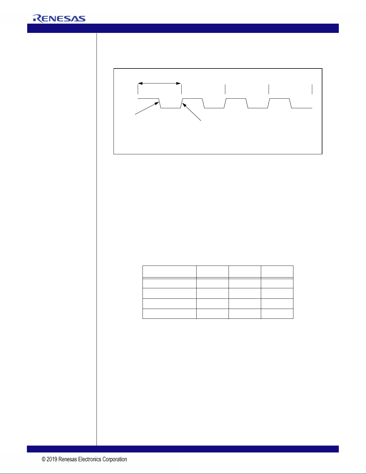
Throughout this manual, when describing signal transitions, the following terminology is used. Rising
edge indicates a low-to-high (0 to 1) transition. Falling edge indicates a high-to-low (1 to 0) transition. These
terms are illustrated in Figure 1.
Figure 1 Signal Transitions
Numeric Representations
To represent numerical values, either decimal, binary, or hexadecimal formats will be used. The binary
format is as follows: 0bDDD, where “D” represents either 0 or 1; the hexadecimal format is as follows:
0xDD, where “D” represents the hexadecimal digit(s); otherwise, it is decimal.
The compressed notation ABC[x|y|z]D refers to ABCxD, ABCyD, and ABCzD.
The compressed notation ABC[x..y]D refers to ABCxD, ABC(x+1)D, ABC(x+2)D,... ABCyD.
Data Units
The following data unit terminology is used in this document.
In quadwords, bit 63 is always the most significant bit and bit 0 is the least significant bit. In double-
words, bit 31 is always the most significant bit and bit 0 is the least significant bit. In words, bit 15 is always
the most significant bit and bit 0 is the least significant bit. In bytes, bit 7 is always the most significant bit
and bit 0 is the least significant bit.
The ordering of bytes within words is referred to as either “big endian” or “little endian.” Big endian
systems label byte zero as the most significant (leftmost) byte of a word. Little endian systems label byte
zero as the least significant (rightmost) byte of a word. See Figure 2.
Ter m Words Bytes Bits
Byte 1/2 1 8
Word 1 2 16
Doubleword (Dword) 2 4 32
Quadword (Qword) 4 8 64
Table 1 Data Unit Terminology
1234
high-to-low
transition low-to-high
transition
single clock cycle

IDT
PES16T4AG2 User Manual 3 May 23, 2013
Notes
Figure 2 Example of Byte Ordering for “Big Endian” or “Little Endian” System Definition
Register Terminology
Software in the context of this register terminology refers to modifications made by PCIe root configura-
tion writes, writes to registers made through the slave SMBus interface, or serial EEPROM register initial-
ization. See Table 2.
Type Abbreviation Description
Hardware Initialized HWINIT Register bits are initialized by firmware or hardware mechanisms
such as pin strapping or serial EEPROM. (System firmware hard-
ware initialization is only allowed for system integrated devices.)
Bits are read-only after initialization and can only be reset (for
write-once by firmware) with reset.
Read Only and Clear RC Software can read the register/bits with this attribute. Reading the
value will automatically cause the register/bit to be reset to zero.
Writing to a RC location has no effect.
Read Clear and Write RCW Software can read the register/bits with this attribute. Reading the
value will automatically cause the register/bits to be reset to zero.
Writes cause the register/bits to be modified.
Reserved Reserved The value read from a reserved register/bit is undefined. Thus,
software must deal correctly with fields that are reserved. On
reads, software must use appropriate masks to extract the defined
bits and not rely on reserved bits being any particular value. On
writes, software must ensure that the values of reserved bit posi-
tions are preserved. That is, the values of reserved bit positions
must first be read, merged with the new values for other bit posi-
tions and then written back.
Read Only RO Software can only read registers/bits with this attribute. Contents
are hardwired to a constant value or are status bits that may be
set and cleared by hardware. Writing to a RO location has no
effect.
Read and Write RW Software can both read and write bits with this attribute.
Table 2 Register Terminology (Sheet 1 of 2)
0123
bit 0bit 31
Address of Bytes within Words: Big Endian
3210
bit 0bit 31
Address of Bytes within Words: Little Endian

IDT
PES16T4AG2 User Manual 4 May 23, 2013
Notes
Use of Hypertext
In Chapter 8, Tables 8.2 and 8.3 contain register names and page numbers highlighted in blue under the
Register Definition column. In pdf files, users can jump from this source table directly to the registers by
clicking on the register name in the source table. Each register name in the table is linked directly to the
appropriate register in the register section of the chapter. To return to the source table after having jumped
to the register section, click on the same register name (in blue) in the register section.
Reference Documents
PCI Express Base Specification, Revision 2.0, PCI Special Interest Group.
PCI Power Management Interface Specification, Revision 1.2, PCI Special Interest Group.
PCI to PCI Bridge Architecture Specification, Revision 1.2, PCI Special Interest Group.
SMBus Specification, Revision 2.0.
Revision History
November 30, 2007: Initial publication of preliminary user manual.
December 4, 2007: Added hardwired address locations for MSMBADDR and SSMBADDR to Chapters
1 and 5.
January 7, 2008: In Chapter 5, I/O Expanders section, added text explaining legacy compatibility with
Gen1 PCIe switches. In Chapter 8, modified the following fields: L0SEL in PCIELCAP has default value of
0x6, ARIS in PCIEDCAP2 is RO, and ARIFEN in PCIEDCTL2 is RO.
January 25, 2008: Removed all reference to REFRES4 and REFRES5 pins.
May 30, 2008: Added Device Number Configuration section to Chapter 1 and added DEVNUMCTL
register to Chapter 8.
July 15, 2008: In Chapter 8. added Autonomous Link Reliability Management section and 4 registers.
Removed General Purpose Register (0x40C).
August 25, 2008: In Chapter 2, deleted reference to FRSTS pins.
Read and Write Clear RW1C Software can read and write to registers/bits with this attribute.
However, writing a value of zero to a bit with this attribute has no
effect. A RW1C bit can only be set to a value of 1 by a hardware
event. To clear a RW1C bit (i.e., change its value to zero) a value
of one must be written to the location. An RW1C bit is never
cleared by hardware.
Read and Write when
Unlocked
RWL Software can read the register/bits with this attribute. Writing to
register/bits with this attribute will only cause the value to be modi-
fied if the REGUNLOCK bit in the SWCTL register is set. When
the REGUNLOCK bit is cleared, writes are ignored and the regis-
ter/bits are effectively read-only.
RWL bits are implicitly “Sitcky.”
Write Transient WT The zero is always read from a bit/field of this type. Writing of a
one is used to quality the writing of other bits/fields in the same
register.
Zero Zero A zero register or bit must be written with a value of zero and
returns a value of zero when read.
Type Abbreviation Description
Table 2 Register Terminology (Sheet 2 of 2)

IDT
PES16T4AG2 User Manual 5 May 23, 2013
Notes
November 3, 2008: In Chapter 1, updated Table 1.2 with additional silicon revisions. Updated the
description for the following fields in Chapter 8: LDIS and LRET in the PCIELCTL register, ULD in the
ALRSTS register, and TLW in the PHYLCFG0 register, and changed the last Reserved field in the
PCIEDCTL2 register from 31:6 to 15:6.
March 30, 2009: In Chapter 5, deleted old Tables 5.1 and 5.11 dealing with master and slave SMBus
addresses.
May 7, 2009: In Chapter 3, revised the Lane Reversal section.
July 21, 2009: In Chapter 3, revised section Dynamic Link Width Reconfiguration Support in the
PES16T4AG2. Also, deleted entire section Software Management of Link Width Upconfiguration and
Downconfiguration.
September 15, 2010: In Table 1.10, changed Buffer type for PCI Express from CML to PCIe differential
and changed reference clocks to HCSL.
October 26, 2010: In Chapter 2, revised Clocking section on page 1 to remove reference to REFCLKM.
May 11, 2011: Deleted all references to DEVNUM field.
September 23, 2011: Added DDDNC (Disable Downstream Device Number Checking) bit to Switch
Control register in Chapter 8, Configuration Registers.
February 22, 2012: Added paragraph after Table 5.11 to explain use of DWord addresses.
January 29, 2013: In Figure 5.8, changed No-ack to Ack between DATALM and DATAUM.
April 30, 2013: In Table 1.6, changed description for PxxMERGEN pins to pull-up via 92K ohm resistor.
In Table 1.9, changed PxxMERGEN pins from pull-down to pull-up.
May 23, 2013: In the Features section of Chapter 1, added reference to SECDED ECC under Reliability,
Availability, Serviceability bullet.

IDT
PES16T4AG2 User Manual 6 May 23, 2013
Notes

Notes
PES16T4AG2 User Manual i May 23, 2013
Table of Contents
®
About This Manual
Introduction ....................................................................................................................................1
Content Summary ..........................................................................................................................1
Signal Nomenclature .....................................................................................................................1
Numeric Representations ..............................................................................................................2
Data Units ......................................................................................................................................2
Register Terminology ..................................................................................................................... 3
Use of Hypertext ............................................................................................................................4
Reference Documents ................................................................................................................... 4
Revision History .............................................................................................................................4
PES16T4AG2 Device Overview
Introduction .....................................................................................................................................1-1
Features..........................................................................................................................................1-1
Logic Diagram — PES16T4AG2.....................................................................................................1-3
Vendor ID........................................................................................................................................1-4
Device ID ........................................................................................................................................1-4
Revision ID......................................................................................................................................1-4
JTAG ID ..........................................................................................................................................1-4
SSID/SSVID....................................................................................................................................1-4
Pin Description................................................................................................................................1-5
Pin Characteristics..........................................................................................................................1-9
Port Configuration.........................................................................................................................1-10
Clocking, Reset and Initialization
Clocking ..........................................................................................................................................2-1
Initialization .....................................................................................................................................2-1
Reset...............................................................................................................................................2-2
Fundamental Reset ................................................................................................................2-2
Hot Reset................................................................................................................................2-4
Upstream Secondary Bus Reset ............................................................................................2-5
Downstream Secondary Bus Reset........................................................................................2-6
Downstream Port Reset Outputs ....................................................................................................2-6
Power Enable Controlled Reset Output..................................................................................2-7
Power Good Controlled Reset Output ....................................................................................2-7
Link Operation
Introduction .....................................................................................................................................3-1
Polarity Inversion ............................................................................................................................ 3-1
Lane Reversal.................................................................................................................................3-1
Link Width Negotiation.................................................................................................................... 3-2
Dynamic Link Width Reconfiguration..............................................................................................3-3
Dynamic Link Width Reconfiguration Support in the PES16T4AG2.......................................3-3
Link Speed Negotiation...................................................................................................................3-4
Link Speed Negotiation in the PES16T4AG2 .........................................................................3-4
Software Management of Link Speed.....................................................................................3-5
Link Reliability.................................................................................................................................3-5

IDT Table of Contents
PES16T4AG2 User Manual ii May 23, 2013
Notes
Autonomous Link Reliability Management .............................................................................3-6
Link Retraining................................................................................................................................ 3-7
Link Down ....................................................................................................................................... 3-8
Slot Power Limit Support ................................................................................................................ 3-8
Upstream Port ........................................................................................................................ 3-8
Downstream Port.................................................................................................................... 3-8
Link States ...................................................................................................................................... 3-8
Active State Power Management ...................................................................................................3-9
Link Status .................................................................................................................................... 3-10
De-emphasis Negotiation ............................................................................................................. 3-10
Low-Swing Transmitter Voltage Mode..........................................................................................3-10
Crosslink ....................................................................................................................................... 3-10
General Purpose I/O
Introduction ..................................................................................................................................... 4-1
GPIO Configuration ........................................................................................................................ 4-1
GPIO Pin Configured as an Input ........................................................................................... 4-1
GPIO Pin Configured as an Output ........................................................................................4-2
GPIO Pin Configured as an Alternate Function...................................................................... 4-2
SMBus Interfaces
Introduction ..................................................................................................................................... 5-1
Master SMBus Interface ................................................................................................................. 5-2
Initialization............................................................................................................................. 5-2
Serial EEPROM...................................................................................................................... 5-2
I/O Expanders.........................................................................................................................5-6
Slave SMBus Interface .................................................................................................................5-13
Initialization........................................................................................................................... 5-14
SMBus Transactions ............................................................................................................ 5-14
Power Management
Introduction ..................................................................................................................................... 6-1
PME Messages............................................................................................................................... 6-2
PCI-Express Power Management Fence Protocol .........................................................................6-2
Power Budgeting Capability............................................................................................................ 6-3
Hot-Plug and Hot-Swap
Hot-Plug.......................................................................................................................................... 7-1
Hot-Plug I/O Expander ...........................................................................................................7-4
Hot-Plug Interrupts and Wake-up ...........................................................................................7-4
Legacy System Hot-Plug Support ..........................................................................................7-5
Hot-Swap ........................................................................................................................................ 7-6
Configuration Registers
Configuration Space Organization.................................................................................................. 8-1
Upstream Port (Port 0) ........................................................................................................... 8-2
Downstream Ports .................................................................................................................. 8-6
Register Definitions.......................................................................................................................8-10
Type 1 Configuration Header Registers ............................................................................... 8-10
PCI Express Capability Structure .........................................................................................8-20
Power Management Capability Structure ............................................................................. 8-36
Message Signaled Interrupt Capability Structure ................................................................. 8-37

IDT Table of Contents
PES16T4AG2 User Manual iii May 23, 2013
Notes
Subsystem ID and Subsystem Vendor ID ............................................................................ 8-39
Extended Configuration Space Access Registers ................................................................8-39
Advanced Error Reporting (AER) Enhanced Capability .......................................................8-40
Device Serial Number Enhanced Capability.........................................................................8-48
PCI Express Virtual Channel Capability ............................................................................... 8-49
Power Budgeting Enhanced Capability ................................................................................8-55
Switch Control and Status Registers ....................................................................................8-56
Autonomous Link Reliability Management ...........................................................................8-71
JTAG Boundary Scan
Introduction ..................................................................................................................................... 9-1
Test Access Point ........................................................................................................................... 9-1
Signal Definitions ............................................................................................................................ 9-1
Boundary Scan Chain..................................................................................................................... 9-3
Test Data Register (DR) ................................................................................................................. 9-4
Boundary Scan Registers.......................................................................................................9-4
Instruction Register (IR).................................................................................................................. 9-6
EXTEST.................................................................................................................................. 9-6
SAMPLE/PRELOAD............................................................................................................... 9-7
BYPASS ................................................................................................................................. 9-7
CLAMP ................................................................................................................................... 9-7
IDCODE.................................................................................................................................. 9-7
VALIDATE .............................................................................................................................. 9-8
RESERVED............................................................................................................................ 9-8
Usage Considerations ............................................................................................................9-8

IDT Table of Contents
PES16T4AG2 User Manual iv May 23, 2013
Notes

Notes
PES16T4AG2 User Manual v May 23, 2013
List of Tables
®
Table 1.1 PES16T4AG2 Device ID......................................................................................................1-4
Table 1.2 PES16T4AG2 Revision ID...................................................................................................1-4
Table 1.3 PCI Express Interface Pins..................................................................................................1-5
Table 1.4 SMBus Interface Pins ..........................................................................................................1-5
Table 1.5 General Purpose I/O Pins....................................................................................................1-6
Table 1.6 System Pins.........................................................................................................................1-6
Table 1.7 Test Pins..............................................................................................................................1-7
Table 1.8 Power, Ground, and SerDes Resistor Pins .........................................................................1-7
Table 1.9 Pin Characteristics...............................................................................................................1-9
Table 2.1 Boot Configuration Vector Signals.......................................................................................2-1
Table 4.1 General Purpose I/O Pin Alternate Function .......................................................................4-1
Table 4.2 GPIO Pin Configuration .......................................................................................................4-1
Table 5.1 PES16T4AG2 Compatible Serial EEPROMs ......................................................................5-2
Table 5.2 Serial EEPROM Initialization Errors ....................................................................................5-5
Table 5.3 I/O Expander Function Allocation ........................................................................................5-6
Table 5.4 I/O Expander Default Output Signal Value ..........................................................................5-7
Table 5.5 I/O Expander 0 Signals......................................................................................................5-10
Table 5.6 I/O Expander 1 Signals......................................................................................................5-10
Table 5.7 I/O Expander 2 Signals......................................................................................................5-12
Table 5.8 I/O Expander 3 Signals......................................................................................................5-12
Table 5.9 I/O Expander 4 Signals......................................................................................................5-13
Table 5.10 Slave SMBus Command Code Fields ............................................................................... 5-14
Table 5.11 CSR Register Read or Write Operation Byte Sequence ...................................................5-15
Table 5.12 CSR Register Read or Write CMD Field Description.........................................................5-15
Table 5.13 Serial EEPROM Read or Write Operation Byte Sequence................................................5-16
Table 5.14 Serial EEPROM Read or Write CMD Field Description.....................................................5-17
Table 6.1 PES16T4AG2 Power Management State Transition Diagram ............................................6-2
Table 8.1 Base Addresses for Port Configuration Space Register......................................................8-1
Table 8.2 Upstream Port 0 Configuration Space Registers.................................................................8-2
Table 8.3 Downstream Ports 1 through 5 Configuration Space Registers ..........................................8-6
Table 9.1 JTAG Pin Descriptions.........................................................................................................9-2
Table 9.2 Boundary Scan Chain..........................................................................................................9-3
Table 9.3 Instructions Supported by PES16T4AG2’s JTAG Boundary Scan......................................9-6
Table 9.4 System Controller Device Identification Register.................................................................9-7

IDT List of Tables
PES16T4AG2 User Manual vi May 23, 2013
Notes

Notes
PES16T4AG2 User Manual vii May 23, 2013
List of Figures
®
Figure 1.1 PES16T4AG2 Architectural Block Diagram .......................................................................1-2
Figure 1.2 PES16T4AG2 Logic Diagram ............................................................................................1-3
Figure 1.3 All Ports Unmerged Configuration ...................................................................................1-11
Figure 1.4 Two Ports Merged Configuration .....................................................................................1-11
Figure 1.5 All Ports Merged Configuration ........................................................................................1-12
Figure 2.1 Fundamental Reset with Serial EEPROM initialization ......................................................2-4
Figure 2.2 Fundamental Reset using RSTHALT to keep device in Quasi-Reset state .......................2-4
Figure 2.3 Power Enable Controlled Reset Output Mode Operation ..................................................2-7
Figure 2.4 Power Good Controlled Reset Output Mode Operation .....................................................2-7
Figure 3.1 Unmerged Port Lane Reversal ..........................................................................................3-1
Figure 3.2 Merged Port Lane Reversal ...............................................................................................3-2
Figure 3.3 PES16T4AG2 ASPM Link Sate Transitions .......................................................................3-9
Figure 5.1 SMBus Interface Configuration Examples .........................................................................5-1
Figure 5.2 Single Double Word Initialization Sequence Format ..........................................................5-3
Figure 5.3 Sequential Double Word Initialization Sequence Format ...................................................5-4
Figure 5.4 Configuration Done Sequence Format ..............................................................................5-4
Figure 5.5 Slave SMBus Command Code Format ............................................................................5-14
Figure 5.6 CSR Register Read or Write CMD Field Format ..............................................................5-15
Figure 5.7 Serial EEPROM Read or Write CMD Field Format ..........................................................5-16
Figure 5.8 CSR Register Read Using SMBus Block Write/Read Transactions with PEC Disabled ..5-17
Figure 5.9 Serial EEPROM Read Using SMBus Block Write/Read Transactions with PEC
Disabled ...........................................................................................................................5-18
Figure 5.10 CSR Register Write Using SMBus Block Write Transactions with PEC Disabled ...........5-18
Figure 5.11 Serial EEPROM Write Using SMBus Block Write Transactions with PEC Disabled ........5-18
Figure 5.12 Serial EEPROM Write Using SMBus Block Write Transactions with PEC Enabled ........5-18
Figure 5.13 CSR Register Read Using SMBus Read and Write Transactions with PEC Disabled ....5-19
Figure 6.1 PES16T4AG2 Power Management State Transition Diagram ...........................................6-1
Figure 7.1 Hot-Plug on Switch Downstream Slots Application ............................................................7-1
Figure 7.2 Hot-Plug with Switch on Add-In Card Application ..............................................................7-2
Figure 7.3 Hot-Plug with Carrier Card Application ..............................................................................7-2
Figure 7.4 PES16T4AG2 Hot-Plug Event Signalling ...........................................................................7-6
Figure 8.1 Port Configuration Space Organization .............................................................................8-2
Figure 9.1 Diagram of the JTAG Logic ................................................................................................9-1
Figure 9.2 State Diagram of PES16T4AG2’s TAP Controller .............................................................9-2
Figure 9.3 Diagram of Observe-only Input Cell ...................................................................................9-4
Figure 9.4 Diagram of Output Cell ......................................................................................................9-5
Figure 9.5 Diagram of Bidirectional Cell ..............................................................................................9-5
Figure 9.6 Device ID Register Format .................................................................................................9-7

IDT List of Figures
PES16T4AG2 User Manual viii May 23, 2013
Notes

Notes
PES16T4AG2 User Manual ix May 23, 2013
Register List
®
AERCAP - AER Capabilities (0x100) ..................................................................................................... 8-40
AERCEM - AER Correctable Error Mask (0x114) .................................................................................. 8-46
AERCES - AER Correctable Error Status (0x110) ................................................................................. 8-45
AERCTL - AER Control (0x118)............................................................................................................. 8-47
AERHL1DW - AER Header Log 1st Doubleword (0x11C) ..................................................................... 8-47
AERHL2DW - AER Header Log 2nd Doubleword (0x120)..................................................................... 8-47
AERHL3DW - AER Header Log 3rd Doubleword (0x124)...................................................................... 8-48
AERHL4DW - AER Header Log 4th Doubleword (0x128)...................................................................... 8-48
AERUEM - AER Uncorrectable Error Mask (0x108) .............................................................................. 8-41
AERUES - AER Uncorrectable Error Status (0x104) ............................................................................. 8-40
AERUESV - AER Uncorrectable Error Severity (0x10C)........................................................................ 8-44
ALRCNT - Autonomous Link Reliability Counter (0x56C) ...................................................................... 8-73
ALRCTL - Autonomous Link Reliability Control (0x560)......................................................................... 8-71
ALRERT - Autonomous Link Reliability Error Rate Threshold (0x5680) ................................................ 8-72
ALRSTS - Autonomous Link Reliability Status (0x564).......................................................................... 8-72
BAR0 - Base Address Register 0 (0x010).............................................................................................. 8-13
BAR1 - Base Address Register 1 (0x014).............................................................................................. 8-14
BCTL - Bridge Control Register (0x03E) ................................................................................................ 8-19
BIST - Built-in Self Test Register (0x00F) .............................................................................................. 8-13
CAPPTR - Capabilities Pointer Register (0x034) ................................................................................... 8-18
CCODE - Class Code Register (0x009) ................................................................................................. 8-12
CLS - Cache Line Size Register (0x00C)............................................................................................... 8-13
DID - Device Identification Register (0x002) .......................................................................................... 8-10
ECFGADDR - Extended Configuration Space Access Address (0x0F8) ............................................... 8-39
ECFGDATA - Extended Configuration Space Access Data (0x0FC)..................................................... 8-40
EEPROMINTF - Serial EEPROM Interface (0x42C) .............................................................................. 8-63
EROMBASE - Expansion ROM Base Address Register (0x038)........................................................... 8-18
GPECTL - General Purpose Event Control (0x450)............................................................................... 8-66
GPESTS - General Purpose Event Status (0x454)................................................................................ 8-66
GPIOCFG - General Purpose I/O Configuration (0x41C)....................................................................... 8-62
GPIOD - General Purpose I/O Data (0x420).......................................................................................... 8-62
GPIOFUNC - General Purpose I/O Control Function (0x418)................................................................ 8-61
HDR - Header Type Register (0x00E).................................................................................................... 8-13
HPCFGCTL - Hot-Plug Configuration Control (0x408)........................................................................... 8-60
INTRLINE - Interrupt Line Register (0x03C)........................................................................................... 8-18
INTRPIN - Interrupt PIN Register (0x03D) ............................................................................................. 8-19
IOBASE - I/O Base Register (0x01C)..................................................................................................... 8-15
IOBASEU - I/O Base Upper Register (0x030)........................................................................................ 8-17
IOEXPADDR0 - SMBus I/O Expander Address 0 (0x434)..................................................................... 8-65
IOEXPADDR1 - SMBus I/O Expander Address 1 (0x438)..................................................................... 8-66
IOEXPINTF - I/O Expander Interface (0x430)........................................................................................ 8-64
IOLIMIT - I/O Limit Register (0x01D)...................................................................................................... 8-15
IOLIMITU - I/O Limit Upper Register (0x032)......................................................................................... 8-18
MBASE - Memory Base Register (0x020).............................................................................................. 8-16
MLIMIT - Memory Limit Register (0x022)............................................................................................... 8-16
MSIADDR - Message Signaled Interrupt Address (0x0D4).................................................................... 8-38
MSICAP - Message Signaled Interrupt Capability and Control (0x0D0) ................................................ 8-37
MSIMDATA - Message Signaled Interrupt Message Data (0x0DC)....................................................... 8-39
MSIUADDR - Message Signaled Interrupt Upper Address (0x0D8) ...................................................... 8-38

IDT Register List
PES16T4AG2 User Manual x May 23, 2013
Notes
PBUSN - Primary Bus Number Register (0x018)....................................................................................8-14
PCICMD - PCI Command Register (0x004)............................................................................................8-10
PCIECAP - PCI Express Capability (0x040) ...........................................................................................8-20
PCIEDCAP - PCI Express Device Capabilities (0x044) ..........................................................................8-21
PCIEDCAP2 - PCI Express Device Capabilities 2 (0x064) .....................................................................8-32
PCIEDCTL - PCI Express Device Control (0x048)..................................................................................8-22
PCIEDCTL2 - PCI Express Device Control 2 (0x068).............................................................................8-33
PCIEDSTS - PCI Express Device Status (0x04A) ..................................................................................8-23
PCIEDSTS2 - PCI Express Device Status 2 (0x06A) .............................................................................8-33
PCIELCAP - PCI Express Link Capabilities (0x04C) ..............................................................................8-24
PCIELCAP2 - PCI Express Link Capabilities 2 (0x06C) .........................................................................8-33
PCIELCTL - PCI Express Link Control (0x050).......................................................................................8-25
PCIELCTL2 - PCI Express Link Control 2 (0x070)..................................................................................8-33
PCIELSTS - PCI Express Link Status (0x052)........................................................................................8-27
PCIELSTS2 - PCI Express Link Status 2 (0x072)...................................................................................8-35
PCIESCAP - PCI Express Slot Capabilities (0x054) ...............................................................................8-28
PCIESCAP2 - PCI Express Slot Capabilities 2 (0x074) ..........................................................................8-35
PCIESCTL - PCI Express Slot Control (0x058).......................................................................................8-30
PCIESCTL2 - PCI Express Slot Control 2 (0x078)..................................................................................8-35
PCIESSTS - PCI Express Slot Status (0x05A) .......................................................................................8-31
PCIESSTS2 - PCI Express Slot Status 2 (0x07A) ..................................................................................8-36
PCIEVCECAP - PCI Express VC Enhanced Capability Header (0x200) ................................................8-49
PCISTS - PCI Status Register (0x006) ...................................................................................................8-11
PHYLCFG0 - Phy Link Configuration 0 (0x530)......................................................................................8-67
PHYLSTATE0 - Phy Link State 0 (0x540)...............................................................................................8-70
PHYLSTS0 - Phy Link Status 0 (0x538)..................................................................................................8-68
PHYPRBS - Phy PRBS Seed (0x55C)....................................................................................................8-71
PLTIMER - Primary Latency Timer (0x00D)............................................................................................8-13
PMBASE - Prefetchable Memory Base Register (0x024) .......................................................................8-16
PMBASEU - Prefetchable Memory Base Upper Register (0x028)..........................................................8-17
PMCAP - PCI Power Management Capabilities (0x0C0)........................................................................8-36
PMCSR - PCI Power Management Control and Status (0x0C4) ............................................................8-37
PMLIMIT - Prefetchable Memory Limit Register (0x026) ........................................................................8-17
PMLIMITU - Prefetchable Memory Limit Upper Register (0x02C) ..........................................................8-17
PVCCAP1- Port VC Capability 1 (0x204)................................................................................................8-49
PVCCAP2- Port VC Capability 2 (0x208)................................................................................................8-50
PVCCTL - Port VC Control (0x20C) ........................................................................................................8-50
PVCSTS - Port VC Status (0x20E) .........................................................................................................8-50
PWRBCAP - Power Budgeting Capabilities (0x280)...............................................................................8-55
PWRBD - Power Budgeting Data (0x288)...............................................................................................8-56
PWRBDSEL - Power Budgeting Data Select (0x284).............................................................................8-55
PWRBDV[7:0] - Power Budgeting Data Value [7:0] (0x300 - 0x31C) .....................................................8-56
PWRBPBC - Power Budgeting Power Budget Capability (0x28C) .........................................................8-56
RID - Revision Identification Register (0x008) ........................................................................................8-12
SBUSN - Secondary Bus Number Register (0x019) ...............................................................................8-14
SECSTS - Secondary Status Register (0x01E) ......................................................................................8-15
SERDESCTL- SerDes Control (0x500)...................................................................................................8-67
SLTIMER - Secondary Latency Timer Register (0x01B).........................................................................8-14
SMBUSCTL - SMBus Control (0x428) ....................................................................................................8-63
SMBUSSTS - SMBus Status (0x424) .....................................................................................................8-62
SNUMCAP - Serial Number Capabilities (0x180) ...................................................................................8-48
SNUMLDW - Serial Number Lower Doubleword (0x184) .......................................................................8-48
SNUMUDW - Serial Number Upper Doubleword (0x188).......................................................................8-48
SSIDSSVID - Subsystem ID and Subsystem Vendor ID (0x0F4) ...........................................................8-39
SSIDSSVIDCAP - Subsystem ID and Subsystem Vendor ID Capability (0x0F0) ...................................8-39

IDT Register List
PES16T4AG2 User Manual xi May 23, 2013
Notes
SUBUSN - Subordinate Bus Number Register (0x01A)..........................................................................8-14
SWCTL - Switch Control (0x404) ............................................................................................................8-57
SWSTS - Switch Status (0x400) .............................................................................................................8-56
VCR0CAP- VC Resource 0 Capability (0x210).......................................................................................8-51
VCR0CTL- VC Resource 0 Control (0x214)............................................................................................8-51
VCR0STS - VC Resource 0 Status (0x218)............................................................................................8-52
VCR0TBL0 - VC Resource 0 Arbitration Table Entry 0 (0x220)..............................................................8-53
VCR0TBL1 - VC Resource 0 Arbitration Table Entry 1 (0x224)..............................................................8-53
VCR0TBL2 - VC Resource 0 Arbitration Table Entry 2 (0x228)..............................................................8-54
VCR0TBL3 - VC Resource 0 Arbitration Table Entry 3 (0x22C).............................................................8-54
VID - Vendor Identification Register (0x000)...........................................................................................8-10

IDT Register List
PES16T4AG2 User Manual xii May 23, 2013
Notes
Table of contents
Other IDT Switch manuals

IDT
IDT 89HPES24N3A User manual

IDT
IDT 89HPES16T4G2 User manual

IDT
IDT 89HPES32NT8xG2 User manual

IDT
IDT Tsi572 User manual

IDT
IDT 89HPES5T5 User manual

IDT
IDT Tsi578 User manual

IDT
IDT PCI Express 89HPES32NT24xG2 User manual

IDT
IDT 89HPES12N3 User manual

IDT
IDT 89HPES24T6G2 User manual

IDT
IDT PowerSpan II User manual


